ICGOO在线商城 > 分立半导体产品 > 晶体管 - FET,MOSFET - 射频 > BF998,215

 Datasheet下载
- 型号: BF998,215
- 制造商: NXP Semiconductors
- 库位|库存: xxxx|xxxx
- 要求:
| 数量阶梯 | 香港交货 | 国内含税 |
| +xxxx | $xxxx | ¥xxxx |
查看当月历史价格
查看今年历史价格
BF998,215产品简介:
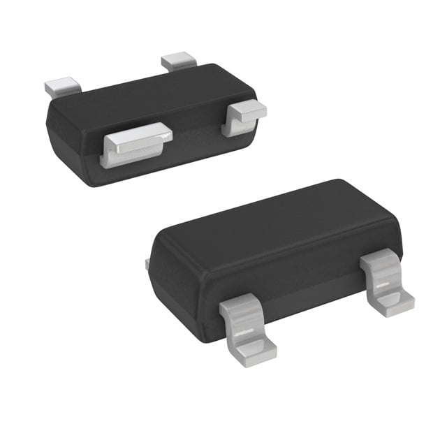
ICGOO电子元器件商城为您提供BF998,215由NXP Semiconductors设计生产,在icgoo商城现货销售,并且可以通过原厂、代理商等渠道进行代购。 BF998,215价格参考。NXP SemiconductorsBF998,215封装/规格:晶体管 - FET,MOSFET - 射频, RF Mosfet N-Channel Dual Gate 8V 10mA 200MHz SOT-143B。您可以下载BF998,215参考资料、Datasheet数据手册功能说明书,资料中有BF998,215 详细功能的应用电路图电压和使用方法及教程。
NXP USA Inc. 的 BF998,215 是一款双栅极N沟道增强型MOSFET,属于射频场效应晶体管(RF FET),广泛应用于高频、低噪声的射频电路中。其主要应用场景包括:

1. 高频低噪声放大器(LNA):BF998,215 具有优异的噪声性能和高增益特性,适用于VHF和UHF频段的接收前端,常用于电视调谐器、FM收音机、无线麦克风和通信接收设备中的低噪声放大。

2. 混频器与变频电路:得益于双栅极结构,该器件可实现良好的信号控制和隔离,适合用作射频混频器,常见于电视、广播接收机和双向无线电系统中,用于频率转换。

3. 便携式与电池供电设备:BF998,215 工作电压低(典型2.5V~6V),功耗小,适合用于手持通信设备、无线传感器和小型无线模块等对功耗敏感的应用。

4. 宽带射频放大:在30MHz至1GHz范围内具有良好的频率响应,可用于宽带信号放大,适用于测试仪器、射频识别(RFID)读写器和业余无线电设备。

5. 工业与消费类电子:广泛用于模拟电视调谐器、CATV设备和汽车音响系统中,提供稳定的射频信号处理能力。

总之,BF998,215 凭借其双栅极设计、低噪声、高增益和低功耗特性,是高频模拟射频电路中的理想选择,尤其适用于需要高性能与小型化的消费电子和通信设备。
| 参数 | 数值 |
| 产品目录 | |
| 描述 | MOSFET NCH DUAL GATE 12V SOT143B射频MOSFET晶体管 N-CH DUAL GATE 12V VHF/UHF |
| 产品分类 | RF FET分离式半导体 |
| Id-ContinuousDrainCurrent | 0.03 A |
| Id-连续漏极电流 | 0.03 A |
| 品牌 | NXP Semiconductors |
| 产品手册 | |
| 产品图片 |
|
| rohs | 符合RoHS无铅 / 符合限制有害物质指令(RoHS)规范要求 |
| 产品系列 | 晶体管,晶体管射频,射频MOSFET晶体管,NXP Semiconductors BF998,215- |
| 数据手册 | |
| 产品型号 | BF998,215 |
| PCN封装 | |
| PCN设计/规格 | |
| Pd-PowerDissipation | 200 mW |
| Pd-功率耗散 | 200 mW |
| Vds-Drain-SourceBreakdownVoltage | 12 V |
| Vds-漏源极击穿电压 | 12 V |
| Vgs-Gate-SourceBreakdownVoltage | +/- 6 V |
| Vgs-栅源极击穿电压 | +/- 6 V |
| 产品目录页面 | |
| 产品种类 | 射频MOSFET晶体管 |
| 产品类型 | RF MOSFET Small Signal |
| 供应商器件封装 | SOT-143B |
| 其它名称 | 568-1973-6 |
| 功率-输出 | - |
| 功率耗散 | 200 mW |
| 包装 | Digi-Reel® |
| 商标 | NXP Semiconductors |
| 噪声系数 | 0.6dB |
| 增益 | - |
| 安装风格 | SMD/SMT |
| 封装 | Reel |
| 封装/外壳 | TO-253-4,TO-253AA |
| 封装/箱体 | SC-61B |
| 工厂包装数量 | 3000 |
| 技术 | MOSFET |
| 晶体管极性 | N-Channel |
| 晶体管类型 | N 通道双门 |
| 最大工作温度 | + 150 C |
| 最小工作温度 | - 65 C |
| 标准包装 | 1 |
| 汲极/源极击穿电压 | 12 V |
| 漏极连续电流 | 0.03 A |
| 电压-测试 | 8V |
| 电压-额定 | 12V |
| 电流-测试 | 10mA |
| 配置 | Single Dual Gate |
| 闸/源击穿电压 | +/- 6 V |
| 零件号别名 | BF998 T/R |
| 频率 | 200MHz |
| 额定电流 | 30mA |


PDF Datasheet 数据手册内容提取
DISCRETE SEMICONDUCTORS DATA SHEET BF998; BF998R Silicon N-channel dual-gate MOS-FETs Product specification 1996 Aug 01 Supersedes data of April 1991
NXP Semiconductors Product specification Silicon N-channel dual-gate MOS-FETs BF998; BF998R FEATURES Short channel transistor with high forward transfer handbook, halfpage d admittance to input capacitance ratio 4 3 Low noise gain controlled amplifier up to 1GHz. g 2 g 1 APPLICATIONS VHF and UHF applications with 12V supply voltage, such as television tuners and professional 1 2 communications equipment. s,b Top view MAM039 DESCRIPTION Marking code: MOp. Depletion type field effect transistor in a plastic Fig.1 Simplified outline (SOT143B) microminiature SOT143B or SOT143R package with and symbol; BF998. source and substrate interconnected. The transistors are protected against excessive input voltage surges by integrated back-to-back diodes between gates and source. d CAUTION handbook, halfpag3e 4 The device is supplied in an antistatic package. The g gate-source input must be protected against static 2 g discharge during transport or handling. 1 PINNING 2 1 PIN SYMBOL DESCRIPTION s,b Top view MAM040 1 s, b source 2 d drain Marking code: MOp. 3 g2 gate2 Fig.2 Simplified outline (SOT143R) 4 g gate1 and symbol; BF998R. 1 QUICK REFERENCE DATA SYMBOL PARAMETER CONDITIONS TYP. MAX. UNIT V drain-source voltage 12 V DS I drain current 30 mA D P total power dissipation 200 mW tot y forward transfer admittance 24 mS fs C input capacitance at gate1 2.1 pF ig1-s C reverse transfer capacitance f=1MHz 25 fF rs F noise figure f=800MHz 1 dB T operating junction temperature 150 C j 1996Aug01 2
NXP Semiconductors Product specification Silicon N-channel dual-gate MOS-FETs BF998; BF998R LIMITING VALUES In accordance with the Absolute Maximum Rating System (IEC 134). SYMBOL PARAMETER CONDITIONS MIN. MAX. UNIT V drain-source voltage 12 V DS I drain current 30 mA D I gate1 current 10 mA G1 I gate2 current 10 mA G2 P total power dissipation; BF998 up to T =60C; seeFig.3; note1 200 mW tot amb up to T =50C; seeFig.3; note2 200 mW amb P total power dissipation; BF998R up to T =50C; seeFig.4; note1 200 mW tot amb T storage temperature 65 +150 C stg T operating junction temperature 150 C j Notes 1. Device mounted on a ceramic substrate, 8mm10 mm0.7mm. 2. Device mounted on a printed-circuit board. MLA198 MGA002 handbook, halfpage handbook, halfpage 200 200 Ptot max (2) (1) Ptot max (mW) (mW) 100 100 0 0 0 100 200 0 100 Tamb( o C) 200 Tamb (°C) (1) Ceramic substrate. (2) Printed-circuit board. Fig.3 Power derating curves; BF998. Fig.4 Power derating curve; BF998R. 1996Aug01 3
NXP Semiconductors Product specification Silicon N-channel dual-gate MOS-FETs BF998; BF998R THERMAL CHARACTERISTICS SYMBOL PARAMETER CONDITIONS VALUE UNIT R thermal resistance from junction to ambient in free air; BF998 note1 460 K/W th j-a note2 500 K/W R thermal resistance from junction to ambient in free air; BF998R note1 500 K/W th j-a Notes 1. Device mounted on a ceramic substrate, 8mm10 mm0.7mm. 2. Device mounted on a printed-circuit board. STATIC CHARACTERISTICS T =25C; unless otherwise specified. j SYMBOL PARAMETER CONDITIONS MIN. MAX. UNIT V gate1-source breakdown voltage V =V =0; I =10mA 6 20 V (BR)G1-SS G2-S DS G1-SS V gate2-source breakdown voltage V =V =0; I =10mA 6 20 V (BR)G2-SS G1-S DS G2-SS V gate1-source cut-off voltage V =4V; V =8V; I =20A 2.0 V (P)G1-S G2-S DS D V gate2-source cut-off voltage V =0; V =8V; I =20A 1.5 V (P)G2-S G1-S DS D I drain-source current V =4V; V =8V; V =0; note1 2 18 mA DSS G2-S DS G1-S I gate1 cut-off current V =V =0; V =5V 50 nA G1-SS G2-S DS G1-S I gate2 cut-off current V =V =0; V =5V 50 nA G2-SS G1-S DS G2-S Note 1. Measured under pulse condition. DYNAMIC CHARACTERISTICS Common source; T =25C; V =8V; V =4V; I =10mA. amb DS G2-S D SYMBOL PARAMETER CONDITIONS MIN. TYP. MAX. UNIT y forward transfer admittance f=1kHz 21 24 mS fs C input capacitance at gate1 f=1MHz 2.1 2.5 pF ig1-s C input capacitance at gate2 f=1MHz 1.2 pF ig2-s C output capacitance f=1MHz 1.05 pF os C reverse transfer capacitance f=1MHz 25 fF rs F noise figure f=200MHz; G =2mS; B =B 0.6 dB S S Sopt f=800MHz; G =3.3mS; B =B 1.0 dB S S Sopt 1996Aug01 4
NXP Semiconductors Product specification Silicon N-channel dual-gate MOS-FETs BF998; BF998R MGE813 MGE815 24 24 han(dmbIDoAo)k, halfpage VG1-S = hand(bmIoDoAk), halfpage VG2-S = 4 V 3 V 2 V 20 0.4 V 20 1 V 0.3 V 16 16 0.2 V 12 0.1 V 12 0 V 8 −0.1 V 8 −0.2 V 0 V 4 −0.3 V 4 −0.4 V −0.5 V 0 0 0 2 4 6 8 10 −1 0 VG1 (V) 1 VDS (V) VG2-S=4V; Tamb=25C. VDS=8V; Tamb=25C. Fig.5 Output characteristics; typical values. Fig.6 Transfer characteristics; typical values. MGE814 MGE811 24 30 handboIDok, halfpage handbook, halfpage 4 V (mA) |yfs| 3 V 20 max typ (mS) 2 V 24 1 V 16 18 12 min 12 8 6 4 VG2-S = 0 V 0.5 V 0 0 −1600 −1200 −800 −400 0 400 0 4 8 12 16 20 VG1 (mV) ID (mA) VDS=8V; VG2-S=4V; Tamb=25C. VDS=8V; Tamb=25C. Fig.7 Drain current as a function of gate1 Fig.8 Forward transfer admittance as a function of voltage; typical values. drain current; typical values. 1996Aug01 5
NXP Semiconductors Product specification Silicon N-channel dual-gate MOS-FETs BF998; BF998R MGE812 MGE810 30 1.5 handbook, halfpage handbook, halfpage |yfs| VG2-S = 4 V Cos (mS) (pF) 24 1.4 3 V 18 1.3 2 V 12 1.2 12 mA 6 1 V 1.1 10 mA 8 mA 0 V 0 1.0 −1 0 1 4 6 8 10 12 14 VG1 (V) VDS (V) VDS=8V; Tamb=25C. VG2-S=4V; f=1MHz; Tamb=25C. Fig.9 Forward transfer admittance as a function of Fig.10 Output capacitance as a function of gate 1 voltage; typical values. drain-source voltage; typical values. MGE809 MBH479 2.3 2.4 handbook, halfpage handbook, halfpage Cis Cis (pF) (pF) 2.1 2.3 1.9 2.2 1.7 2.1 1.5 1.3 2.0 −2.4 −1.6 −0.8 0 0.8 6 4 2 0 −2 VG1-S (V) VG2−S (V) VDS=8V; VG2-S=4V; f=1MHz; Tamb=25C. VDS=8V; VG1-S=0V; f=1MHz; Tamb=25C. Fig.11 Gate 1 input capacitance as a function of Fig.12 Gate 1 input capacitance as a function of gate 1-source voltage; typical values. gate 2-source voltage; typical values. 1996Aug01 6
NXP Semiconductors Product specification Silicon N-channel dual-gate MOS-FETs BF998; BF998R MGC466 MGC467 10 103 103 yis yrs ϕ rs (mS) (μS) (deg) bis ϕ 1 102 rs 102 yrs 10 1 10 10 gis 10 2 1 1 10 102 f (MHz) 103 10 102 f (MHz) 103 VDS=8V; VG2-S=4V; ID=10mA; Tamb=25C. VDS=8V; VG2-S=4V; ID=10mA; Tamb=25C. Fig.13 Input admittance as a function of the Fig.14 Reverse transfer admittance and phase as a frequency; typical values. function of frequency; typical values. MGC468 MGC469 102 102 10 yos yfs ϕ fs (mS) bos (mS) yfs (deg) 1 10 ϕ 10 fs gos 10 1 1 1 10 2 10 102 f (MHz) 103 10 102 f (MHz) 103 VDS=8V; VG2-S=4V; ID=10mA; Tamb=25C. VDS=8V; VG2-S=4V; ID=10mA; Tamb=25C. Fig.15 Forward transfer admittance and phase as a Fig.16 Output admittance as a function of the function of frequency; typical values. frequency; typical values. 1996Aug01 7
NXP Semiconductors Product specification Silicon N-channel dual-gate MOS-FETs BF998; BF998R handbook, full pagewidth VDD 47 μF Vagc 1 nF 1 nF 20 μH 1 nF 1 nF 47 kΩ 1.8 kΩ 50 Ω L2 output 1 nF C1 5.5 pF 50 Ω 1 nF input 15 pF 360 Ω 10 pF L1 140 kΩ VDD 1 nF DBB1405 330 kΩ DBB2405 330 kΩ 100 kΩ 1 nF 1 nF Vtun Vtun input output MGE802 VDD=12V; GS=2mS; GL=0.5mS. L1=45nH; 4turns 0.8mm copper wire, internal diameter 4mm. L2=160nH; 3turns 0.8mm copper wire, internal diameter 8mm. Tapped at approximately half a turn from the cold side, to adjust GL=0.5mS. C1 adjusted for GS=2mS. Fig.17 Gain control test circuit at f=200MHz. 1996Aug01 8
NXP Semiconductors Product specification Silicon N-channel dual-gate MOS-FETs BF998; BF998R handbook, full pagewidth VDD Vagc VDD 1 nF 1 nF 140 kΩ 100 kΩ 1 nF 270 kΩ L4 L1 1 nF L3 1 nF 50 Ω output 1 nF L2 50 Ω 1 nF C3 C4 input 0.5 to 4 to 40 pF 3.5 pF C1 C2 2 to 18 pF 0.5 to 3.5 pF MGE801 1.8 kΩ 360 Ω VDD VDD=12V; GS=3.3mS; GL=1mS. L1=L4=200nH; 11 turns 0.5mm copper wire, without spacing, internal diameter 3mm. L2=2cm, silvered 0.8mm copper wire, 4mm above ground plane. L3=2cm, silvered 0.5mm copper wire, 4mm above ground plane. Fig.18 Gain control test circuit at f=800MHz. 1996Aug01 9
NXP Semiconductors Product specification Silicon N-channel dual-gate MOS-FETs BF998; BF998R MGE808 MGE807 0 0 handboΔoGk,t rhalfpage handboΔoGk,t rhalfpage (dB) (dB) IDSS = −10 −10 max typ min −20 −20 −30 −30 −40 IDSS = −40 max typ min −50 −50 0 2 4 6 8 10 0 2 4 6 8 10 Vagc (V) Vagc (V) VDD=12V; f=200MHz; Tamb=25C. VDD=12V; f=800MHz; Tamb=25C. Fig.19 Automatic gain control characteristics Fig.20 Automatic gain control characteristics measured in circuit of Fig.17. measured in circuit of Fig.18. 1996Aug01 10
NXP Semiconductors Product specification Silicon N-channel dual-gate MOS-FETs BF998; BF998R PACKAGE OUTLINES Plastic surface-mounted package; 4 leads SOT143B D B E A X y v M A HE e bp w M B 4 3 Q A A1 c 1 2 Lp b1 e1 detail X 0 1 2 mm scale DIMENSIONS (mm are the original dimensions) UNIT A mAa1x bp b1 c D E e e1 HE Lp Q v w y 1.1 0.48 0.88 0.15 3.0 1.4 2.5 0.45 0.55 mm 0.1 1.9 1.7 0.2 0.1 0.1 0.9 0.38 0.78 0.09 2.8 1.2 2.1 0.15 0.45 OUTLINE REFERENCES EUROPEAN ISSUE DATE VERSION IEC JEDEC JEITA PROJECTION 04-11-16 SOT143B 06-03-16 1996Aug01 11
NXP Semiconductors Product specification Silicon N-channel dual-gate MOS-FETs BF998; BF998R Plastic surface-mounted package; reverse pinning; 4 leads SOT143R D B E A X y v M A HE e bp w M B 3 4 Q A A1 c 2 1 Lp b1 e1 detail X 0 1 2 mm scale DIMENSIONS (mm are the original dimensions) UNIT A A1 bp b1 c D E e e1 HE Lp Q v w y max 1.1 0.48 0.88 0.15 3.0 1.4 2.5 0.55 0.45 mm 0.1 1.9 1.7 0.2 0.1 0.1 0.9 0.38 0.78 0.09 2.8 1.2 2.1 0.25 0.25 OUTLINE REFERENCES EUROPEAN ISSUE DATE VERSION IEC JEDEC JEITA PROJECTION 04-11-16 SOT143R SC-61AA 06-03-16 1996Aug01 12
NXP Semiconductors Product specification Silicon N-channel dual-gate MOS-FETs BF998; BF998R DATA SHEET STATUS DOCUMENT PRODUCT DEFINITION STATUS(1) STATUS(2) Objective data sheet Development This document contains data from the objective specification for product development. Preliminary data sheet Qualification This document contains data from the preliminary specification. Product data sheet Production This document contains the product specification. Notes 1. Please consult the most recently issued document before initiating or completing a design. 2. The product status of device(s) described in this document may have changed since this document was published and may differ in case of multiple devices. The latest product status information is available on the Internet at URLhttp://www.nxp.com. DEFINITIONS Right to make changes NXP Semiconductors reserves the right to make changes to information Product specification The information and data published in this document, including without limitation provided in a Product data sheet shall define the specifications and product descriptions, at any time and specification of the product as agreed between NXP without notice. This document supersedes and replaces all Semiconductors and its customer, unless NXP information supplied prior to the publication hereof. Semiconductors and customer have explicitly agreed otherwise in writing. In no event however, shall an Suitability for use NXP Semiconductors products are agreement be valid in which the NXP Semiconductors not designed, authorized or warranted to be suitable for product is deemed to offer functions and qualities beyond use in life support, life-critical or safety-critical systems or those described in the Product data sheet. equipment, nor in applications where failure or malfunction of an NXP Semiconductors product can reasonably be expected to result in personal injury, death or severe DISCLAIMERS property or environmental damage. NXP Semiconductors Limited warranty and liability Information in this accepts no liability for inclusion and/or use of NXP document is believed to be accurate and reliable. Semiconductors products in such equipment or However, NXP Semiconductors does not give any applications and therefore such inclusion and/or use is at representations or warranties, expressed or implied, as to the customer’s own risk. the accuracy or completeness of such information and Applications Applications that are described herein for shall have no liability for the consequences of use of such any of these products are for illustrative purposes only. information. NXP Semiconductors makes no representation or In no event shall NXP Semiconductors be liable for any warranty that such applications will be suitable for the indirect, incidental, punitive, special or consequential specified use without further testing or modification. damages (including - without limitation - lost profits, lost Customers are responsible for the design and operation of savings, business interruption, costs related to the their applications and products using NXP removal or replacement of any products or rework Semiconductors products, and NXP Semiconductors charges) whether or not such damages are based on tort accepts no liability for any assistance with applications or (including negligence), warranty, breach of contract or any customer product design. It is customer’s sole other legal theory. responsibility to determine whether the NXP Notwithstanding any damages that customer might incur Semiconductors product is suitable and fit for the for any reason whatsoever, NXP Semiconductors’ customer’s applications and products planned, as well as aggregate and cumulative liability towards customer for for the planned application and use of customer’s third the products described herein shall be limited in party customer(s). Customers should provide appropriate accordance with the Terms and conditions of commercial design and operating safeguards to minimize the risks sale of NXP Semiconductors. associated with their applications and products. 1996Aug01 13
NXP Semiconductors Product specification Silicon N-channel dual-gate MOS-FETs BF998; BF998R NXP Semiconductors does not accept any liability related Export control This document as well as the item(s) to any default, damage, costs or problem which is based described herein may be subject to export control on any weakness or default in the customer’s applications regulations. Export might require a prior authorization from or products, or the application or use by customer’s third national authorities. party customer(s). Customer is responsible for doing all Quick reference data The Quick reference data is an necessary testing for the customer’s applications and extract of the product data given in the Limiting values and products using NXP Semiconductors products in order to Characteristics sections of this document, and as such is avoid a default of the applications and the products or of not complete, exhaustive or legally binding. the application or use by customer’s third party customer(s). NXP does not accept any liability in this Non-automotive qualified products Unless this data respect. sheet expressly states that this specific NXP Semiconductors product is automotive qualified, the Limiting values Stress above one or more limiting product is not suitable for automotive use. It is neither values (as defined in the Absolute Maximum Ratings qualified nor tested in accordance with automotive testing System of IEC60134) will cause permanent damage to or application requirements. NXP Semiconductors accepts the device. Limiting values are stress ratings only and no liability for inclusion and/or use of non-automotive (proper) operation of the device at these or any other qualified products in automotive equipment or conditions above those given in the Recommended applications. operating conditions section (if present) or the Characteristics sections of this document is not warranted. In the event that customer uses the product for design-in Constant or repeated exposure to limiting values will and use in automotive applications to automotive permanently and irreversibly affect the quality and specifications and standards, customer (a) shall use the reliability of the device. product without NXP Semiconductors’ warranty of the product for such automotive applications, use and Terms and conditions of commercial sale NXP specifications, and (b) whenever customer uses the Semiconductors products are sold subject to the general product for automotive applications beyond NXP terms and conditions of commercial sale, as published at Semiconductors’ specifications such use shall be solely at http://www.nxp.com/profile/terms, unless otherwise customer’s own risk, and (c) customer fully indemnifies agreed in a valid written individual agreement. In case an NXP Semiconductors for any liability, damages or failed individual agreement is concluded only the terms and product claims resulting from customer design and use of conditions of the respective agreement shall apply. NXP the product for automotive applications beyond NXP Semiconductors hereby expressly objects to applying the Semiconductors’ standard warranty and NXP customer’s general terms and conditions with regard to the Semiconductors’ product specifications. purchase of NXP Semiconductors products by customer. No offer to sell or license Nothing in this document may be interpreted or construed as an offer to sell products that is open for acceptance or the grant, conveyance or implication of any license under any copyrights, patents or other industrial or intellectual property rights. 1996Aug01 14
NXP Semiconductors provides High Performance Mixed Signal and Standard Product solutions that leverage its leading RF, Analog, Power Management, Interface, Security and Digital Processing expertise Customer notification This data sheet was changed to reflect the new company name NXP Semiconductors, including new legal definitions and disclaimers. No changes were made to the technical content, except for package outline drawings which were updated to the latest version. Contact information For additional information please visit: http://www.nxp.com For sales offices addresses send e-mail to: salesaddresses@nxp.com © NXP B.V. 2010 All rights are reserved. Reproduction in whole or in part is prohibited without the prior written consent of the copyright owner. The information presented in this document does not form part of any quotation or contract, is believed to be accurate and reliable and may be changed without notice. No liability will be accepted by the publisher for any consequence of its use. Publication thereof does not convey nor imply any license under patent- or other industrial or intellectual property rights. Printed in The Netherlands R77/02/pp15 Date of release:1996Aug01