ICGOO在线商城 > 分立半导体产品 > 晶体管 - FET,MOSFET - 射频 > 2N5485
 Datasheet下载
- 型号: 2N5485
- 制造商: Central Semiconductor
- 库位|库存: xxxx|xxxx
- 要求:
| 数量阶梯 | 香港交货 | 国内含税 |
| +xxxx | $xxxx | ¥xxxx |
查看当月历史价格
查看今年历史价格
2N5485产品简介:
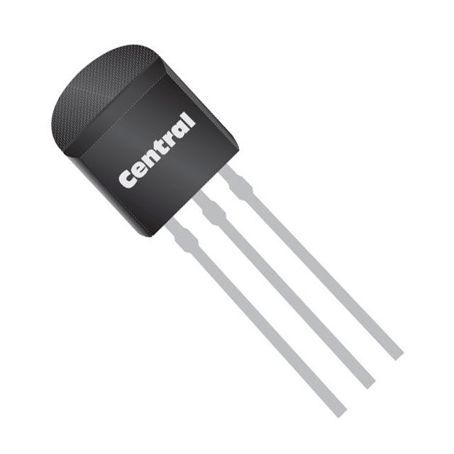
ICGOO电子元器件商城为您提供2N5485由Central Semiconductor设计生产,在icgoo商城现货销售,并且可以通过原厂、代理商等渠道进行代购。 2N5485价格参考¥4.25-¥6.80。Central Semiconductor2N5485封装/规格:晶体管 - FET,MOSFET - 射频, 射频 Mosfet N 通道 JFET 15V 4mA 20dB TO-92。您可以下载2N5485参考资料、Datasheet数据手册功能说明书,资料中有2N5485 详细功能的应用电路图电压和使用方法及教程。
2N5485是由Central Semiconductor Corp生产的射频晶体管,属于FET(场效应晶体管)中的MOSFET类别。该型号主要用于高频和射频应用领域,具有低噪声、高增益和良好的线性特性,适合于需要高性能信号处理的场景。以下是其主要应用场景:

1. 射频放大器:2N5485常用于射频信号放大电路中,特别是在低噪声放大器(LNA)设计中。它能够有效提升弱信号的强度,同时保持较低的噪声水平,适用于无线通信、广播接收和其他射频系统。

2. 混频器和调制器:在射频前端模块中,2N5485可以作为混频器或调制器的核心元件,用于频率转换或信号调制。它的高线性度有助于减少失真,提高信号质量。

3. 振荡器:该器件可用于构建射频振荡器电路,生成稳定的高频信号。其优异的高频性能使其成为本地振荡器或其他高频信号源的理想选择。

4. 开关应用:2N5485也可用作射频开关,控制信号路径的选择。它能够在不同频率的信号之间快速切换,适用于多频段通信设备。

5. 无线通信设备:包括对讲机、无线麦克风、遥控器等小型无线设备中,2N5485可用于信号的放大和处理,提供可靠的射频性能。

6. 业余无线电:由于其出色的射频特性,2N5485广泛应用于业余无线电爱好者自制的收发信机和实验电路中。

总的来说,2N5485凭借其高频性能和低噪声特点,非常适合用于各种射频和高频电子设备的设计与开发,尤其是在需要高灵敏度和低失真的应用场景中表现出色。
| 参数 | 数值 |
| Id-ContinuousDrainCurrent | 30 mA |
| Id-连续漏极电流 | 30 mA |
| 品牌 | Central Semiconductor |
| 产品目录 | 半导体 |
| 描述 | JFET N-Chan JFET |
| 产品分类 | 分离式半导体 |
| 产品手册 | |
| 产品图片 |
|
| rohs | 过渡期间 |
| 产品系列 | 晶体管,JFET,Central Semiconductor 2N5485 |
| 产品型号 | 2N5485 |
| Pd-PowerDissipation | 310 mW |
| Pd-功率耗散 | 310 mW |
| Vds-Drain-SourceBreakdownVoltage | 25 V |
| Vds-漏源极击穿电压 | 25 V |
| Vgs-Gate-SourceBreakdownVoltage | 25 V |
| Vgs-栅源极击穿电压 | 25 V |
| Vgs=0时的漏-源电流 | 4 mA to 10 mA |
| 产品种类 | JFET |
| 功率耗散 | 310 mW |
| 商标 | Central Semiconductor |
| 安装风格 | Through Hole |
| 封装 | Bulk |
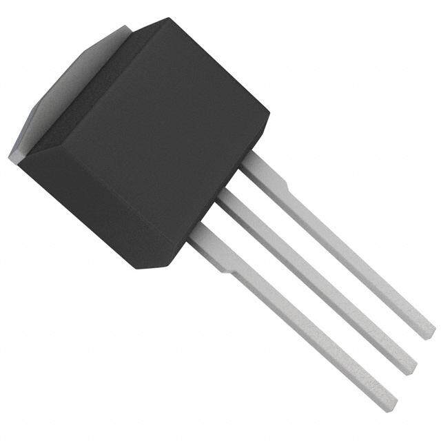
| 封装/箱体 | TO-92 |
| 工厂包装数量 | 2500 |
| 晶体管极性 | N-Channel |
| 漏极连续电流 | 30 mA |
| 漏源电压VDS | 25 V |
| 系列 | 2N5485 |
| 配置 | Single |
| 闸/源击穿电压 | 25 V |


- 商务部:美国ITC正式对集成电路等产品启动337调查
- 曝三星4nm工艺存在良率问题 高通将骁龙8 Gen1或转产台积电
- 太阳诱电将投资9.5亿元在常州建新厂生产MLCC 预计2023年完工
- 英特尔发布欧洲新工厂建设计划 深化IDM 2.0 战略
- 台积电先进制程称霸业界 有大客户加持明年业绩稳了
- 达到5530亿美元!SIA预计今年全球半导体销售额将创下新高
- 英特尔拟将自动驾驶子公司Mobileye上市 估值或超500亿美元
- 三星加码芯片和SET,合并消费电子和移动部门,撤换高东真等 CEO
- 三星电子宣布重大人事变动 还合并消费电子和移动部门
- 海关总署:前11个月进口集成电路产品价值2.52万亿元 增长14.8%
,TO-226_straightlead.jpg)


PDF Datasheet 数据手册内容提取
2N5484 2N5485 2N5486 www.centralsemi.com The CENTRAL SEMICONDUCTOR 2N5484, 2N5485, SILICON and 2N5486 are silicon N-Channel JFETs designed for N-CHANNEL JFET RF amplifier and mixer applications. These devices will operate well in the VHF/UHF frequency range. MARKING: FULL PART NUMBER TO-92 CASE MAXIMUM RATINGS: (TA=25°C) SYMBOL UNITS Drain-Gate Voltage VDG 25 V Gate-Source Voltage VGS 25 V Drain Current ID 30 mA Continuous Gate Current IG 10 mA Power Dissipation PD 310 mW Operating and Storage Junction Temperature TJ, Tstg -65 to +150 °C ELECTRICAL CHARACTERISTICS: (TA=25°C unless otherwise noted) 2N5484 2N5485 2N5486 SYMBOL TEST CONDITIONS MIN MAX MIN MAX MIN MAX UNITS IGSS VGS=20V - 1.0 - 1.0 - 1.0 nA IGSS VGS=20V, TA=100°C - 0.2 - 0.2 - 0.2 μA IDSS VDS=15V 1.0 5.0 4.0 10 8.0 20 mA BVGSS IG=1.0μA 25 - 25 - 25 - V VGS(off) VDS=15V, ID=10nA 0.3 3.0 0.5 4.0 2.0 6.0 V |yfs| VDS=15V, VGS=0, f=1.0kHz 3.0 6.0 3.5 7.0 4.0 8.0 mS |yos| VDS=15V, VGS=0, f=1.0kHz - 50 - 60 - 75 μS Ciss VDS=15V, VGS=0, f=1.0MHz - 5.0 - 5.0 - 5.0 pF Coss VDS=15V, VGS=0, f=1.0MHz - 2.0 - 2.0 - 2.0 pF Crss VDS=15V, VGS=0, f=1.0MHz - 1.0 - 1.0 - 1.0 pF Re(yis) VDS=15V, VGS=0, f=100MHz - 100 - - - - μS Re(yis) VDS=15V, VGS=0, f=400MHz - - - 1.0 - 1.0 mS Re(yos) VDS=15V, VGS=0, f=100MHz - 75 - - - - μS Re(yos) VDS=15V, VGS=0, f=400MHz - - - 100 - 100 μS Re(yfs) VDS=15V, VGS=0, f=100MHz 2.5 - - - - - mS Re(yfs) VDS=15V, VGS=0, f=400MHz - - 3.0 - 3.5 - mS R1 (2-May 2014)
2N5484 2N5485 2N5486 SILICON N-CHANNEL JFET ELECTRICAL CHARACTERISTICS: (TA=25°C unless otherwise noted) 2N5484 2N5485 2N5486 SYMBOL TEST CONDITIONS MIN MAX MIN MAX MIN MAX UNITS NF VDS=15V, VGS=0, RG=1MΩ, f=1.0KHz - 2.5 - 2.5 - 2.5 dB NF VDS=15V, ID=1.0mA, RG=1KΩ, f=100MHz - 3.0 - - - - dB NF VDS=15V, ID=1.0mA, RG=1KΩ, f=200MHz - 4.0TYP - - - - dB NF VDS=15V, ID=4.0mA, RG=1KΩ, f=100MHz - - - 2.0 - 2.0 dB NF VDS=15V, ID=4.0mA, RG=1KΩ, f=400MHz - - - 4.0 - 4.0 dB GPS VDS=15V, ID=1.0mA, f=100MHz 16 25 - - - - dB GPS VDS=15V, ID=1.0mA, f=200MHz - 14 TYP - - - - dB GPS VDS=15V, ID=4.0mA, f=100MHz - - 18 30 18 30 dB GPS VDS=15V, ID=4.0mA, f=400MHz - - 10 20 10 20 dB TO-92 CASE - MECHANICAL OUTLINE LEAD CODE: 1) Drain 2) Source 3) Gate MARKING: FULL PART NUMBER R1 (2-May 2014) www.centralsemi.com
OUTSTANDING SUPPORT AND SUPERIOR SERVICES PRODUCT SUPPORT Central’s operations team provides the highest level of support to insure product is delivered on-time. • Supply management (Customer portals) • Custom bar coding for shipments • Inventory bonding • Custom product packing • Consolidated shipping options DESIGNER SUPPORT/SERVICES Central’s applications engineering team is ready to discuss your design challenges. Just ask. • Free quick ship samples (2nd day air) • Special wafer diffusions • Online technical data and parametric search • PbSn plating options • SPICE models • Package details • Custom electrical curves • Application notes • Environmental regulation compliance • Application and design sample kits • Customer specific screening • Custom product and package development • Up-screening capabilities REQUESTING PRODUCT PLATING 1. If requesting Tin/Lead plated devices, add the suffix “ TIN/LEAD” to the part number when ordering (example: 2N2222A TIN/LEAD). 2. If requesting Lead (Pb) Free plated devices, add the suffix “ PBFREE” to the part number when ordering (example: 2N2222A PBFREE). CONTACT US Corporate Headquarters & Customer Support Team Central Semiconductor Corp. 145 Adams Avenue Worldwide Field Representatives: Hauppauge, NY 11788 USA www.centralsemi.com/wwreps Main Tel: (631) 435-1110 Main Fax: (631) 435-1824 Worldwide Distributors: Support Team Fax: (631) 435-3388 www.centralsemi.com/wwdistributors www.centralsemi.com For the latest version of Central Semiconductor’s LIMITATIONS AND DAMAGES DISCLAIMER, which is part of Central’s Standard Terms and Conditions of sale, visit: www.centralsemi.com/terms www.centralsemi.com (001)
PDN01067 10/03/17 N/A http://www.centralsemi.com N/A Please be advised that Central Semiconductor must immediately discontinue the product(s) listed in the attached PDN notice. We are unable to accept any further orders for these products u__n_le_s_s we have available inventory on hand. You may have purchased one or more of the products listed. Please do not hesitate to contact your local Central Semiconductor sales representative with any questions or needs you may have. Central regrets any inconvenience this may cause. Sincerely, Central Semiconductor Corp.
PDN01067 10/03/17 N/A http://www.centralsemi.com N/A Summary:The 2N5485 silicon N-Channel JFET is discontinued and is now classified as End of Life (EOL). Although Central Semiconductor Corp. makes every effort to continue to produce devices that have been proclaimed EOL (End of Life) by various manufacturers, it is an accepted industry practice to discontinue certain devices when customer demand falls below a minimum level of sustainability. Accordingly, the following product(s) have been transitioned to End of Life status as part of Central's Product Management Process. Any replacement product will be noted below. The effective date for placing the last purchase order will be six(6) months from the date of this notice and twelve(12) months from the notice date for final shipments; this may be extended if inventory is available. C__en_t_r_al_ P_a_r_t_ N_u_m_b_e_r_ _ _ R__ep_l_a_ce_m__en_t_ _ _ _ _ _ _ _ _ 2N5485 2N5486 H Central would be happy to assist you by providing additional information or technical data to help locate an alternate source if we have no replacement available. Please email your requests to engineering@centralsemi.com.