ICGOO在线商城 > 分立半导体产品 > 晶体管 - FET,MOSFET - 射频 > MMBFJ309

 Datasheet下载
- 型号: MMBFJ309
- 制造商: Fairchild Semiconductor
- 库位|库存: xxxx|xxxx
- 要求:
| 数量阶梯 | 香港交货 | 国内含税 |
| +xxxx | $xxxx | ¥xxxx |
查看当月历史价格
查看今年历史价格
MMBFJ309产品简介:
ICGOO电子元器件商城为您提供MMBFJ309由Fairchild Semiconductor设计生产,在icgoo商城现货销售,并且可以通过原厂、代理商等渠道进行代购。 MMBFJ309价格参考。Fairchild SemiconductorMMBFJ309封装/规格:晶体管 - FET,MOSFET - 射频, RF Mosfet N-Channel JFET 10V 10mA 450MHz 12dB SOT-23-3。您可以下载MMBFJ309参考资料、Datasheet数据手册功能说明书,资料中有MMBFJ309 详细功能的应用电路图电压和使用方法及教程。
ON Semiconductor 的 MMBFJ309 是一款N沟道结型场效应晶体管(JFET),属于射频MOSFET类别,常用于小信号放大和高频开关应用。该器件采用SOT-23小型封装,适合高密度电路设计。

MMBFJ309 主要应用于射频(RF)和模拟电路中,常见使用场景包括:
1. 射频放大器:在无线通信系统中作为低噪声放大器(LNA),用于接收前端,提升微弱信号的信噪比,适用于FM收音机、对讲机、无线麦克风等设备。
2. 信号开关与调制电路:利用其快速开关特性,在射频信号路径中实现通断控制,广泛用于通信模块中的信号路由切换。
3. 振荡器与混频器:在高频振荡电路和谐波产生电路中,凭借良好的跨导特性和稳定性,用于构建本地振荡源或频率转换电路。
4. 消费类电子产品:如便携式音频设备、遥控装置、蓝牙模块等,因其低功耗和高频率响应而被选用。
5. 工业与汽车电子:用于传感器信号调理、车载通信系统等对可靠性要求较高的环境。

MMBFJ309 具有低栅极漏电流、高输入阻抗和良好的温度稳定性,适合处理小信号且需保持信号完整性的场合。由于其为JFET结构,无需持续栅极电流驱动,控制简单,特别适用于高阻抗输入级设计。

综上,MMBFJ309 是一款高性能的小信号射频FET,广泛用于通信、消费电子及工业领域的高频模拟电路中,尤其适合空间受限但要求稳定性能的便携式设备。
| 参数 | 数值 |
| 产品目录 | |
| 描述 | IC SWITCH RF N-CH 25V 10MA SOT23射频JFET晶体管 NCh RF Transistor |
| 产品分类 | RF FET分离式半导体 |
| Id-连续漏极电流 | 30 mA |
| 品牌 | Fairchild Semiconductor |
| 产品手册 | |
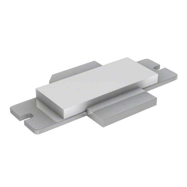
| 产品图片 |
|
| rohs | 符合RoHS无铅 / 符合限制有害物质指令(RoHS)规范要求 |
| 产品系列 | 晶体管,晶体管射频,射频JFET晶体管,Fairchild Semiconductor MMBFJ309- |
| 数据手册 | |
| 产品型号 | MMBFJ309 |
| PCN封装 | |
| PCN设计/规格 | |
| Pd-PowerDissipation | 350 mW |
| Pd-功率耗散 | 350 mW |
| Vds-Drain-SourceBreakdownVoltage | 25 V |
| Vds-漏源极击穿电压 | 25 V |
| Vgs-Gate-SourceBreakdownVoltage | - 25 V |
| Vgs-栅源极击穿电压 | - 25 V |
| Vgs=0时的漏-源电流 | 30 mA to 80 mA |
| 产品 | RF JFET |
| 产品培训模块 | http://www.digikey.cn/PTM/IndividualPTM.page?site=cn&lang=zhs&ptm=356 |
| 产品种类 | 射频JFET晶体管 |
| 供应商器件封装 | SOT-23-3(TO-236) |
| 其它名称 | MMBFJ309DKR |
| 功率-输出 | - |
| 功率耗散 | 350 mW |
| 包装 | Digi-Reel® |
| 单位重量 | 60 mg |
| 商标 | Fairchild Semiconductor |
| 噪声系数 | 3dB |
| 增益 | 12dB |
| 安装风格 | SMD/SMT |
| 封装 | Reel |
| 封装/外壳 | TO-236-3,SC-59,SOT-23-3 |
| 封装/箱体 | SOT-23 |
| 工作温度范围 | - 55 C to + 150 C |
| 工厂包装数量 | 3000 |
| 技术 | Silicon |
| 晶体管极性 | N-Channel |
| 晶体管类型 | N 通道 JFET |
| 最大工作温度 | + 150 C |
| 最小工作温度 | - 55 C |
| 标准包装 | 1 |
| 正向跨导-最小值 | 0.01 S to 0.02 S |
| 漏源电压VDS | 25 V |
| 电压-测试 | 10V |
| 电压-额定 | 25V |
| 电流-测试 | 10mA |
| 类型 | Silicon |
| 系列 | MMBFJ309 |
| 配置 | Single |
| 闸/源击穿电压 | - 25 V |
| 闸/源截止电压 | - 4 V |
| 零件号别名 | MMBFJ309_NL |
| 频率 | 450MHz |
| 额定电流 | 30mA |


.jpg)

- 商务部:美国ITC正式对集成电路等产品启动337调查
- 曝三星4nm工艺存在良率问题 高通将骁龙8 Gen1或转产台积电
- 太阳诱电将投资9.5亿元在常州建新厂生产MLCC 预计2023年完工
- 英特尔发布欧洲新工厂建设计划 深化IDM 2.0 战略
- 台积电先进制程称霸业界 有大客户加持明年业绩稳了
- 达到5530亿美元!SIA预计今年全球半导体销售额将创下新高
- 英特尔拟将自动驾驶子公司Mobileye上市 估值或超500亿美元
- 三星加码芯片和SET,合并消费电子和移动部门,撤换高东真等 CEO
- 三星电子宣布重大人事变动 还合并消费电子和移动部门
- 海关总署:前11个月进口集成电路产品价值2.52万亿元 增长14.8%


PDF Datasheet 数据手册内容提取
Is Now Part of To learn more about ON Semiconductor, please visit our website at www.onsemi.com Please note: As part of the Fairchild Semiconductor integration, some of the Fairchild orderable part numbers will need to change in order to meet ON Semiconductor’s system requirements. Since the ON Semiconductor product management systems do not have the ability to manage part nomenclature that utilizes an underscore (_), the underscore (_) in the Fairchild part numbers will be changed to a dash (-). This document may contain device numbers with an underscore (_). Please check the ON Semiconductor website to verify the updated device numbers. The most current and up-to-date ordering information can be found at www.onsemi.com. Please email any questions regarding the system integration to Fairchild_questions@onsemi.com. ON Semiconductor and the ON Semiconductor logo are trademarks of Semiconductor Components Industries, LLC dba ON Semiconductor or its subsidiaries in the United States and/or other countries. ON Semiconductor owns the rights to a number of patents, trademarks, copyrights, trade secrets, and other intellectual property. A listing of ON Semiconductor’s product/patent coverage may be accessed at www.onsemi.com/site/pdf/Patent-Marking.pdf. ON Semiconductor reserves the right to make changes without further notice to any products herein. ON Semiconductor makes no warranty, representation or guarantee regarding the suitability of its products for any particular purpose, nor does ON Semiconductor assume any liability arising out of the application or use of any product or circuit, and specifically disclaims any and all liability, including without limitation special, consequential or incidental damages. Buyer is responsible for its products and applications using ON Semiconductor products, including compliance with all laws, regulations and safety requirements or standards, regardless of any support or applications information provided by ON Semiconductor. “Typical” parameters which may be provided in ON Semiconductor data sheets and/or specifications can and do vary in different applications and actual performance may vary over time. All operating parameters, including “Typicals” must be validated for each customer application by customer’s technical experts. ON Semiconductor does not convey any license under its patent rights nor the rights of others. ON Semiconductor products are not designed, intended, or authorized for use as a critical component in life support systems or any FDA Class 3 medical devices or medical devices with a same or similar classification in a foreign jurisdiction or any devices intended for implantation in the human body. Should Buyer purchase or use ON Semiconductor products for any such unintended or unauthorized application, Buyer shall indemnify and hold ON Semiconductor and its officers, employees, subsidiaries, affiliates, and distributors harmless against all claims, costs, damages, and expenses, and reasonable attorney fees arising out of, directly or indirectly, any claim of personal injury or death associated with such unintended or unauthorized use, even if such claim alleges that ON Semiconductor was negligent regarding the design or manufacture of the part. ON Semiconductor is an Equal Opportunity/Affirmative Action Employer. This literature is subject to all applicable copyright laws and is not for resale in any manner.
M M B January 2015 F J 3 0 9 / M MMBFJ309 / MMBFJ310 M B F N-Channel RF Amplifier J 3 1 0 — N Description - C G h This device is designed for VHF/UHF amplifier, oscil- a n lator and mixer applications. As a common gate n amplifier, 16 dB at 100 MHz and 12 dB at 450 MHz S e l can be realized. Sourced from process 92. Source & SOT-23 Note: Source & Drain R Drain are interchangeable. D are interchangeable F A m Ordering Information p l i f i e Part Number Top Mark Package Packing Method r MMBFJ309 6U SOT-23 3L Tape and Reel MMBFJ310 6T SOT-23 3L Tape and Reel Absolute Maximum Ratings(1), (2) Stresses exceeding the absolute maximum ratings may damage the device. The device may not function or be opera- ble above the recommended operating conditions and stressing the parts to these levels is not recommended. In addi- tion, extended exposure to stresses above the recommended operating conditions may affect device reliability. The absolute maximum ratings are stress ratings only. Values are at T = 25°C unless otherwise noted. A Symbol Parameter Value Unit V Drain-Gate Voltage 25 V DG V Gate-Source Voltage -25 V GS I Forward Gate Current 10 mA GF T , T Operating and Storage Junction Temperature Range -55 to 150 °C J STG Notes: 1. These ratings are based on a maximum junction temperature of 150°C. 2. These are steady-state limits. Fairchild Semiconductor should be consulted on applications involving pulsed or low-duty-cycle operations. Thermal Characteristics(3) Values are at T = 25°C unless otherwise noted. A Symbol Parameter Max. Unit Total Device Dissipation 350 mW P D Derate Above 25°C 2.8 mW/°C RθJA Thermal Resistance, Junction-to-Ambient 357 °C/W Note: 3. Device mounted on FR-4 PCB 36mm × 18mm × 1.5mm; mounting pad for the collector lead minimum 6cm2. © 1997 Fairchild Semiconductor Corporation www.fairchildsemi.com MMBFJ309 / MMBFJ310 Rev. 1.5
M M Electrical Characteristics B F Values are at TA = 25°C unless otherwise noted. J 3 0 Symbol Parameter Conditions Min. Typ. Max. Unit 9 Off Characteristics / M V Gate-Source Breakdown Voltage I = -1.0 μA, V = 0 -25 V M (BR)GSS G DS B VGS = -15 V, VDS = 0 -1.0 nA F IGSS Gate Reverse Current VGS = -15 V, VDS = 0, TA = 125°C -1.0 μA J3 1 MMBFJ309 -1.0 -4.0 0 VGS(off) Gate-Source Cut-Off Voltage VDS = 10 V, ID = 1.0 nA V — MMBFJ310 -2.0 -6.5 N On Characteristics - C Zero-Gate Voltage Drain MMBFJ309 12 30 h IDSS Current(4) VDS = 10 V, VGS = 0 MMBFJ310 24 60 mA an n V Gate-Source Forward Voltage V = 0, I = 1.0 mA 1.0 V e GS(f) DS G l Small Signal Characteristics R F Common-Source Input V = 10 V, I = 10 mA, MMBFJ309 0.7 A Re DS D mmhos (yis) Conductance f = 100 MHz MMBFJ310 0.5 m p Re Common-Source Output V = 10 V, I = 10 mA, f = 100 MHz 0.25 mmhos lif (yos) Conductance DS D ie r G Common-Gate Power Gain V = 10 V, I = 10 mA, f = 100 MHz 16 dB pg DS D Common-Source Forward Re V = 10 V, I = 10 mA, f = 100 MHz 12 mmhos (yfs) Transconductance DS D Common-Gate Input Re V = 10 V, I = 10 mA, f = 100 MHz 12 mmhos (yig) Conductance DS D Common-Source Forward V = 10 V, I = 10 mA, MMBFJ309 10000 20000 g DS D μmhos fs Transconductance f = 1.0 kHz MMBFJ310 8000 18000 Common-Source Output g V = 10 V, I = 10 mA, f = 1.0 kHz 150 μmhos oss Conductance DS D Common-Gate Forward V = 10 V, I = 10 mA, MMBFJ309 13000 g DS D μmhos fg Conductance f = 1.0 kHz MMBFJ310 12000 Common-Gate Output V = 10 V, I = 10 mA, MMBFJ309 100 g DS D μmhos og Conductance f = 1.0 kHz MMBFJ310 150 C Drain-Gate Capacitance V = 0, V = -10 V, f = 1.0 MHz 2.0 2.5 pF dg DS GS C Source-Gate Capacitance V = 0, V = -10 V, f = 1.0 MHz 4.1 5.0 pF sg DS GS NF Noise Figure V = 10 V, I = 10 mA, f = 450 MHz 3.0 dB DS D Equivalent Short-Circuit Input en Noise Voltage VDS = 10 V, ID = 10 mA, f = 100 Hz 6.0 nV/ Hz Note: 4. Pulse test: pulse width ≤ 300 μs, duty cycle ≤ 2.0% © 1997 Fairchild Semiconductor Corporation www.fairchildsemi.com MMBFJ309 / MMBFJ310 Rev. 1.5 2
M M Typical Performance Characteristics B F J 3 0 9 / M M B F J 3 1 0 — N - C h a n n e l Figure 1. Transfer Characteristics Figure 2. Transfer Characteristics R F A m p l i f i e r Figure 3. Transfer Characteristics Figure 4. Transfer Characteristics Figure 5. Input Admittance Figure 6. Forward Transadmittance © 1997 Fairchild Semiconductor Corporation www.fairchildsemi.com MMBFJ309 / MMBFJ310 Rev. 1.5 3
M M Typical Performance Characteristics (Continued) B F J 3 0 9 / M M B F J 3 1 0 — N - C h a n n e l R F Figure 7. Common Drain-Source Figure 8. Output Conductance vs. Drain Current A m p l i f i e r Figure 9. Output Admittance Figure 10. Capacitance vs. Voltage Figure 11. Noise Voltage vs. Frequency Figure 12. Reverse Transadmittance © 1997 Fairchild Semiconductor Corporation www.fairchildsemi.com MMBFJ309 / MMBFJ310 Rev. 1.5 4
M M Typical Performance Characteristics (Continued) B F J 3 0 9 / M M B F J 3 1 0 — N - C h a n n e l R F Figure 13. Parameter Interactions Figure 14. Transconductance vs. Drain Current A m p l i f i e r 700 W) m 600 N ( TIO 500 SIPA 400 SOT-23 S DI 300 R E W 200 O P - PD100 0 0 25 50 75 100 125 150 TEMPERATURE ( o C) Figure 15. Leakage Current vs. Voltage Figure 16. Power Dissipation vs. Ambient Temperature © 1997 Fairchild Semiconductor Corporation www.fairchildsemi.com MMBFJ309 / MMBFJ310 Rev. 1.5 5
M M Physical Dimensions B F J 3 0 9 / M 2.92±0.20 0.95 M B F 3 J 1.40 3 1 0 — +0.20 1.30 2.20 -0.15 N - C h a n 1 2 n (0.29) 0.60 e 0.95 0.37 l R 0.20 A B 1.00 F 1.90 1.90 A m LAND PATTERN p RECOMMENDATION l i f i e 1.20 MAX SEE DETAIL A r (0.93) 0.10 0.00 0.10 C C 2.40±0.30 NOTES: UNLESS OTHERWISE SPECIFIED GAGE PLANE A) REFERENCE JEDEC REGISTRATION TO-236, VARIATION AB, ISSUE H. 0.23 B) ALL DIMENSIONS ARE IN MILLIMETERS. 0.08 C) DIMENSIONS ARE INCLUSIVE OF BURRS, 0.25 MOLD FLASH AND TIE BAR EXTRUSIONS. D) DIMENSIONING AND TOLERANCING PER ASME Y14.5M - 1994. 0.20 MIN SEATING E) DRAWING FILE NAME: MA03DREV10 (0.55) PLANE SCALE: 2X Figure 17. 3-LEAD, SOT23, JEDEC TO-236, LOW PROFILE © 1997 Fairchild Semiconductor Corporation www.fairchildsemi.com MMBFJ309 / MMBFJ310 Rev. 1.5 6
TRADEMARKS The following includes registered and unregistered trademarks and service marks, owned by Fairchild Semiconductor and/or its global subsidiaries, and is not intended to be an exhaustive list of all such trademarks. AccuPower(cid:165) F-PFS(cid:165) OPTOPLANAR® AttitudeEngine™ FRFET® ®* Awinda® Global Power ResourceSM ® TinyBoost® AX-CAP®* GreenBridge(cid:165) PowerTrench® TinyBuck® BitSiC(cid:165) Green FPS(cid:165) PowerXS™ TinyCalc(cid:165) Build it Now(cid:165) Green FPS(cid:165) e-Series(cid:165) Programmable Active Droop(cid:165) TinyLogic® CorePLUS(cid:165) Gmax(cid:165) QFET® TINYOPTO(cid:165) CorePOWER(cid:165) GTO(cid:165) QS(cid:165) TinyPower(cid:165) CROSSVOLT(cid:165) IntelliMAX(cid:165) Quiet Series(cid:165) TinyPWM(cid:165) CTL(cid:165) ISOPLANAR(cid:165) RapidConfigure(cid:165) TinyWire(cid:165) Current Transfer Logic(cid:165) Making Small Speakers Sound Louder (cid:165) TranSiC(cid:165) DEUXPEED® and Better™ TriFault Detect(cid:165) Dual Cool™ MegaBuck(cid:165) Saving our world, 1mW/W/kW at a time™ TRUECURRENT®* EcoSPARK® MICROCOUPLER(cid:165) SignalWise(cid:165) μSerDes(cid:165) EfficientMax(cid:165) MicroFET(cid:165) SmartMax(cid:165) ESBC(cid:165) MicroPak(cid:165) SMART START(cid:165) ® MicroPak2(cid:165) SSoPlMut®ions for Your Success(cid:165) UHC® Fairchild® MillerDrive(cid:165) STEALTH(cid:165) Ultra FRFET(cid:165) FFFFFAAAaasiCCSrtcTvTThC®® iQlodur eSie(cid:165)et mSiecroiensd(cid:165)uctor® MMMMMmTToVWotixNt®iiS®oo®nnaGMveraird®x®(cid:165) SSSSSuuuuupppppeereeerrrrSFMSSOEOOOTTTTS(cid:165)®(cid:165)(cid:165)®-3--68 XUVVVXsCioSnseli™XutFnaa(cid:165)Esg l™MTe(cid:165)Palxu(cid:165)s(cid:165) FETBench(cid:165) SyncFET(cid:165) FPS(cid:165) OOpPtToOHLiTO(cid:165)GIC® Sync-Lock™ (cid:3037)(cid:10106)™ * Trademarks of System General Corporation, used under license by Fairchild Semiconductor. DISCLAIMER FAIRCHILD SEMICONDUCTOR RESERVES THE RIGHT TO MAKE CHANGES WITHOUT FURTHER NOTICE TO ANY PRODUCTS HEREIN TO IMPROVE RELIABILITY, FUNCTION, OR DESIGN. TO OBTAIN THE LATEST, MOST UP-TO-DATE DATASHEET AND PRODUCT INFORMATION, VISIT OUR WEBSITE AT HTTP://WWW.FAIRCHILDSEMI.COM.FAIRCHILD DOES NOT ASSUME ANY LIABILITY ARISING OUT OF THE APPLICATION OR USE OF ANY PRODUCT OR CIRCUIT DESCRIBED HEREIN; NEITHER DOES IT CONVEY ANY LICENSE UNDER ITS PATENT RIGHTS, NOR THE RIGHTS OF OTHERS. THESE SPECIFICATIONS DO NOT EXPAND THE TERMS OF FAIRCHILD’S WORLDWIDE TERMS AND CONDITIONS, SPECIFICALLY THE WARRANTY THEREIN, WHICH COVERS THESE PRODUCTS. LIFE SUPPORT POLICY FAIRCHILD’S PRODUCTS ARE NOT AUTHORIZED FOR USE AS CRITICAL COMPONENTS IN LIFE SUPPORT DEVICES OR SYSTEMS WITHOUT THE EXPRESS WRITTEN APPROVAL OF FAIRCHILD SEMICONDUCTOR CORPORATION. As used herein: 1. Life support devices or systems are devices or systems which, (a) are 2. A critical component in any component of a life support, device, or intended for surgical implant into the body or (b) support or sustain system whose failure to perform can be reasonably expected to life, and (c) whose failure to perform when properly used in cause the failure of the life support device or system, or to affect its accordance with instructions for use provided in the labeling, can be safety or effectiveness. reasonably expected to result in a significant injury of the user. ANTI-COUNTERFEITING POLICY Fairchild Semiconductor Corporation's Anti-Counterfeiting Policy. Fairchild's Anti-Counterfeiting Policy is also stated on our external website, www.fairchildsemi.com, under Sales Support. Counterfeiting of semiconductor parts is a growing problem in the industry. All manufacturers of semiconductor products are experiencing counterfeiting of their parts. Customers who inadvertently purchase counterfeit parts experience many problems such as loss of brand reputation, substandard performance, failed applications, and increased cost of production and manufacturing delays. Fairchild is taking strong measures to protect ourselves and our customers from the proliferation of counterfeit parts. Fairchild strongly encourages customers to purchase Fairchild parts either directly from Fairchild or from Authorized Fairchild Distributors who are listed by country on our web page cited above. Products customers buy either from Fairchild directly or from Authorized Fairchild Distributors are genuine parts, have full traceability, meet Fairchild's quality standards for handling and storage and provide access to Fairchild's full range of up-to-date technical and product information. Fairchild and our Authorized Distributors will stand behind all warranties and will appropriately address any warranty issues that may arise. Fairchild will not provide any warranty coverage or other assistance for parts bought from Unauthorized Sources. Fairchild is committed to combat this global problem and encourage our customers to do their part in stopping this practice by buying direct or from authorized distributors. PRODUCT STATUS DEFINITIONS Definition of Terms Datasheet Identification Product Status Definition Datasheet contains the design specifications for product development. Specifications may change Advance Information Formative / In Design in any manner without notice. Datasheet contains preliminary data; supplementary data will be published at a later date. Fairchild Preliminary First Production Semiconductor reserves the right to make changes at any time without notice to improve design. Datasheet contains final specifications. Fairchild Semiconductor reserves the right to make No Identification Needed Full Production changes at any time without notice to improve the design. Datasheet contains specifications on a product that is discontinued by Fairchild Semiconductor. Obsolete Not In Production The datasheet is for reference information only. Rev. I73 © Fairchild Semiconductor Corporation www.fairchildsemi.com
ON Semiconductor and are trademarks of Semiconductor Components Industries, LLC dba ON Semiconductor or its subsidiaries in the United States and/or other countries. ON Semiconductor owns the rights to a number of patents, trademarks, copyrights, trade secrets, and other intellectual property. A listing of ON Semiconductor’s product/patent coverage may be accessed at www.onsemi.com/site/pdf/Patent−Marking.pdf. ON Semiconductor reserves the right to make changes without further notice to any products herein. ON Semiconductor makes no warranty, representation or guarantee regarding the suitability of its products for any particular purpose, nor does ON Semiconductor assume any liability arising out of the application or use of any product or circuit, and specifically disclaims any and all liability, including without limitation special, consequential or incidental damages. Buyer is responsible for its products and applications using ON Semiconductor products, including compliance with all laws, regulations and safety requirements or standards, regardless of any support or applications information provided by ON Semiconductor. “Typical” parameters which may be provided in ON Semiconductor data sheets and/or specifications can and do vary in different applications and actual performance may vary over time. All operating parameters, including “Typicals” must be validated for each customer application by customer’s technical experts. ON Semiconductor does not convey any license under its patent rights nor the rights of others. ON Semiconductor products are not designed, intended, or authorized for use as a critical component in life support systems or any FDA Class 3 medical devices or medical devices with a same or similar classification in a foreign jurisdiction or any devices intended for implantation in the human body. Should Buyer purchase or use ON Semiconductor products for any such unintended or unauthorized application, Buyer shall indemnify and hold ON Semiconductor and its officers, employees, subsidiaries, affiliates, and distributors harmless against all claims, costs, damages, and expenses, and reasonable attorney fees arising out of, directly or indirectly, any claim of personal injury or death associated with such unintended or unauthorized use, even if such claim alleges that ON Semiconductor was negligent regarding the design or manufacture of the part. ON Semiconductor is an Equal Opportunity/Affirmative Action Employer. This literature is subject to all applicable copyright laws and is not for resale in any manner. PUBLICATION ORDERING INFORMATION LITERATURE FULFILLMENT: N. American Technical Support: 800−282−9855 Toll Free ON Semiconductor Website: www.onsemi.com Literature Distribution Center for ON Semiconductor USA/Canada 19521 E. 32nd Pkwy, Aurora, Colorado 80011 USA Europe, Middle East and Africa Technical Support: Order Literature: http://www.onsemi.com/orderlit Phone: 303−675−2175 or 800−344−3860 Toll Free USA/Canada Phone: 421 33 790 2910 Fax: 303−675−2176 or 800−344−3867 Toll Free USA/Canada Japan Customer Focus Center For additional information, please contact your local Email: orderlit@onsemi.com Phone: 81−3−5817−1050 Sales Representative © Semiconductor Components Industries, LLC www.onsemi.com www.onsemi.com 1
Mouser Electronics Authorized Distributor Click to View Pricing, Inventory, Delivery & Lifecycle Information: O N Semiconductor: MMBFJ309_Q MMBFJ309