ICGOO在线商城 > 分立半导体产品 > 晶体管 - FET,MOSFET - 射频 > PD57018STR-E
 Datasheet下载
- 型号: PD57018STR-E
- 制造商: STMicroelectronics
- 库位|库存: xxxx|xxxx
- 要求:
| 数量阶梯 | 香港交货 | 国内含税 |
| +xxxx | $xxxx | ¥xxxx |
查看当月历史价格
查看今年历史价格
PD57018STR-E产品简介:
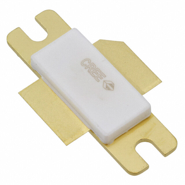
ICGOO电子元器件商城为您提供PD57018STR-E由STMicroelectronics设计生产,在icgoo商城现货销售,并且可以通过原厂、代理商等渠道进行代购。 PD57018STR-E价格参考。STMicroelectronicsPD57018STR-E封装/规格:晶体管 - FET,MOSFET - 射频, RF Mosfet LDMOS 28V 100mA 945MHz 16.5dB 18W PowerSO-10RF (Straight Lead)。您可以下载PD57018STR-E参考资料、Datasheet数据手册功能说明书,资料中有PD57018STR-E 详细功能的应用电路图电压和使用方法及教程。
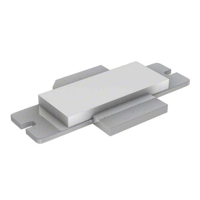
STMicroelectronics的PD57018STR-E是一款射频MOSFET(金属氧化物半导体场效应晶体管),属于射频功率晶体管类别,主要用于高频信号放大和射频功率处理。该器件广泛应用于无线通信系统中的射频功率放大模块。

典型应用场景包括:工业、科学和医疗(ISM)频段设备,如433 MHz、915 MHz等频段的无线传输系统;低功率射频发射机;无线传感器网络;远程遥测与遥控系统;以及短距离无线通信设备(如RFID读写器、无线门禁、智能抄表等)。由于其具备良好的增益、效率和热稳定性,PD57018STR-E适合在需要稳定射频输出的小型化电子设备中使用。

此外,该器件采用紧凑的表面贴装封装(如SOT-223或类似形式),便于集成于高密度PCB设计中,适用于对空间要求严格的嵌入式应用。因其工作频率范围适中、驱动简单,也常用于替代分立元件搭建的射频放大电路,提升系统可靠性和生产一致性。

总之,PD57018STR-E主要面向中低功率射频放大需求,在物联网、自动化控制和无线数据传输等领域具有广泛应用价值。
| 参数 | 数值 |
| 产品目录 | |
| 描述 | TRANSISTOR RF POWERSO-10 |
| 产品分类 | RF FET |
| 品牌 | STMicroelectronics |
| 数据手册 | |
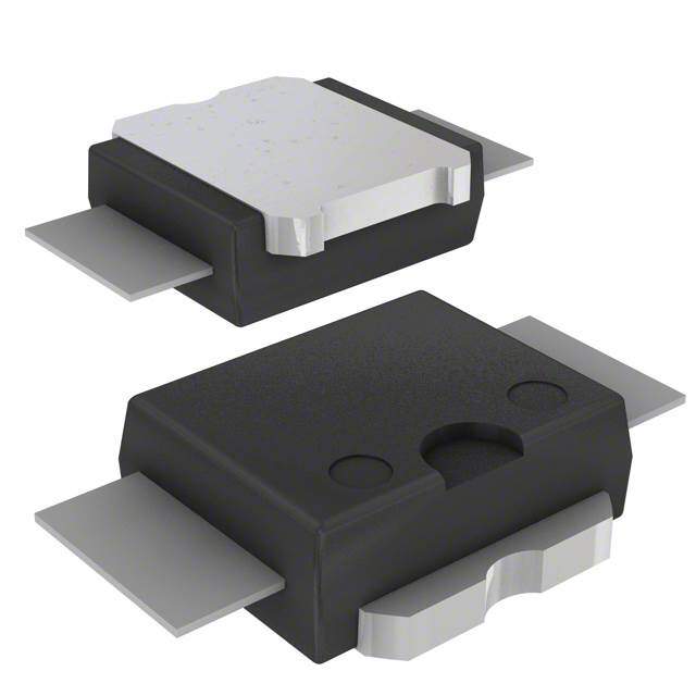
| 产品图片 |
|
| 产品型号 | PD57018STR-E |
| rohs | 无铅 / 符合限制有害物质指令(RoHS)规范要求 |
| 产品系列 | - |
| 产品目录页面 | |
| 供应商器件封装 | PowerSO-10RF(直引线) |
| 其它名称 | 497-6476-1 |
| 其它有关文件 | http://www.st.com/web/catalog/sense_power/FM1987/CL1989/SC1829/PF131340?referrer=70071840 |
| 功率-输出 | 18W |
| 包装 | 剪切带 (CT) |
| 噪声系数 | - |
| 增益 | 16.5dB |
| 封装/外壳 | PowerSO-10 裸露底部焊盘 |
| 晶体管类型 | LDMOS |
| 标准包装 | 1 |
| 电压-测试 | 28V |
| 电压-额定 | 65V |
| 电流-测试 | 100mA |
| 频率 | 945MHz |
| 额定电流 | 2.5A |
.jpg)


- 商务部:美国ITC正式对集成电路等产品启动337调查
- 曝三星4nm工艺存在良率问题 高通将骁龙8 Gen1或转产台积电
- 太阳诱电将投资9.5亿元在常州建新厂生产MLCC 预计2023年完工
- 英特尔发布欧洲新工厂建设计划 深化IDM 2.0 战略
- 台积电先进制程称霸业界 有大客户加持明年业绩稳了
- 达到5530亿美元!SIA预计今年全球半导体销售额将创下新高
- 英特尔拟将自动驾驶子公司Mobileye上市 估值或超500亿美元
- 三星加码芯片和SET,合并消费电子和移动部门,撤换高东真等 CEO
- 三星电子宣布重大人事变动 还合并消费电子和移动部门
- 海关总署:前11个月进口集成电路产品价值2.52万亿元 增长14.8%


PDF Datasheet 数据手册内容提取
PD57018-E RF POWER transistor, LdmoST plastic family N-channel enhancement-mode, lateral MOSFETs Features ■ Excellent thermal stability ■ Common source configuration ■ P = 18 W with 16.5dB gain@945 MHz/28 V OUT ■ New RF plastic package PowerSO-10RF Description (formed lead) The device is a common source N-channel, enhancement-mode lateral field-effect RF power transistor. It is designed for high gain, broad band commercial and industrial applications. It operates at 28 V in common source mode at frequencies of up to 1 GHz. The device boasts the excellent gain, linearity and reliability of ST’s latest LDMOS technology mounted in the first true SMD plastic PowerSO-10RF (straight lead) RF power package, PowerSO-10RF. Device’s superior linearity performance makes it an ideal solution for base station applications. The PowerSO-10 plastic package, designed to offer Figure 1. Pin connection high reliability, is the first ST JEDEC approved, Source high power SMD package. It has been specially optimized for RF needs and offers excellent RF performance and ease of assembly. Mounting recommendations are available in www.st.com/rf/ (look for application note AN1294). Gate Drain Table 1. Device summary Order code Package Packing PD57018-E PowerSO-10RF (formed lead) Tube PD57018S-E PowerSO-10RF (straight lead) Tube PD57018TR-E PowerSO-10RF (formed lead) Tape and reel PD57018STR-E PowerSO-10RF (straight lead) Tape and reel December 2010 Doc ID 12214 Rev 5 1/25 www.st.com 25
Contents PD57018-E Contents 1 Electrical data . . . . . . . . . . . . . . . . . . . . . . . . . . . . . . . . . . . . . . . . . . . . . . 3 1.1 Maximum ratings . . . . . . . . . . . . . . . . . . . . . . . . . . . . . . . . . . . . . . . . . . . . 3 1.2 Thermal data . . . . . . . . . . . . . . . . . . . . . . . . . . . . . . . . . . . . . . . . . . . . . . . 3 2 Electrical characteristics . . . . . . . . . . . . . . . . . . . . . . . . . . . . . . . . . . . . . 4 2.1 Static . . . . . . . . . . . . . . . . . . . . . . . . . . . . . . . . . . . . . . . . . . . . . . . . . . . . . 4 2.2 Dynamic . . . . . . . . . . . . . . . . . . . . . . . . . . . . . . . . . . . . . . . . . . . . . . . . . . . 4 2.3 Moisture sensitivity level . . . . . . . . . . . . . . . . . . . . . . . . . . . . . . . . . . . . . . . 4 3 Impedance . . . . . . . . . . . . . . . . . . . . . . . . . . . . . . . . . . . . . . . . . . . . . . . . . 5 4 Typical performance . . . . . . . . . . . . . . . . . . . . . . . . . . . . . . . . . . . . . . . . . 6 4.1 PD57018-E . . . . . . . . . . . . . . . . . . . . . . . . . . . . . . . . . . . . . . . . . . . . . . . . . 6 4.2 PD57018S-E . . . . . . . . . . . . . . . . . . . . . . . . . . . . . . . . . . . . . . . . . . . . . . . 8 5 Test circuit . . . . . . . . . . . . . . . . . . . . . . . . . . . . . . . . . . . . . . . . . . . . . . . . 10 6 Circuit layout . . . . . . . . . . . . . . . . . . . . . . . . . . . . . . . . . . . . . . . . . . . . . . 12 7 Common source s-parameter . . . . . . . . . . . . . . . . . . . . . . . . . . . . . . . . 13 8 Package mechanical data . . . . . . . . . . . . . . . . . . . . . . . . . . . . . . . . . . . . 19 9 Revision history . . . . . . . . . . . . . . . . . . . . . . . . . . . . . . . . . . . . . . . . . . . 24 2/25 Doc ID 12214 Rev 5
PD57018-E Electrical data 1 Electrical data 1.1 Maximum ratings Table 2. Absolute maximum ratings (T = 25°C) CASE Symbol Parameter Value Unit V Drain-source voltage 65 V (BR)DSS V Gate-source voltage ± 20 V GS I Drain current 2.5 A D P Power dissipation (@ T = 70°C) 31.7 W DISS C T Max. operating junction temperature 165 °C J T Storage temperature -65 to +150 °C STG 1.2 Thermal data Table 3. Thermal data Symbol Parameter Value Unit R Junction - case thermal resistance 3.0 °C/W thJC Doc ID 12214 Rev 5 3/25
Electrical characteristics PD57018-E 2 Electrical characteristics T = +25 oC CASE 2.1 Static Table 4. Static Symbol Test conditions Min Typ Max Unit V V = 0 I = 10 mA 65 V (BR)DSS GS DS I V = 0 V = 28 V 1 μA DSS GS DS I V = 20 V V = 0 V 1 μA GSS GS DS V V = 28 V I = 100 mA 2.0 4.0 V GS(Q) DS D R V = 10 V I = 1.25 A 0.76 Ω DS(on) GS D g V = 10 V I = 1 A 1 mho FS DS D C V = 0 V = 28 V f = 1 MHz 34.5 pF ISS GS DS C V = 0 V = 28 V f = 1 MHz 21 pF OSS GS DS C V = 0 V = 28 V f = 1 MHz 1.3 pF RSS GS DS 2.2 Dynamic Table 5. Dynamic Symbol Test conditions Min Typ Max Unit P V = 28 V, I = 100 mA f = 945 MHz 18 W OUT DD DQ G V = 28 V, I = 100 mA, P = 18 W, f = 945 MHz 14 16.5 dB PS DD DQ OUT h V = 28 V, I = 100 mA, P = 18 W, f = 945 MHz 50 53 % D DD DQ OUT Load V = 28 V, I = 100 mA, P = 18 W, f = 945 MHz DD DQ OUT 10:1 VSWR mismatch All phase angles 2.3 Moisture sensitivity level T able 6. Moisture sensitivity level Test methodology Rating J-STD-020B MSL 3 4/25 Doc ID 12214 Rev 5
PD57018-E Impedance 3 Impedance Figure 2. Current conventions Table 7. Impedance data PD57018-E PD57018S-E Freq. (MHz) Z (Ω) Z (Ω) Freq. (MHz) Z (Ω) Z (Ω) IN DL IN DL 925 .52 - j 1.75 3.04 + j .10 925 .35 - j .53 1.92 + j 4.13 945 .49 - j 2.38 3.14 + j .76 945 .53 - j .86 2.03 + j 2.81 960 .48 - j 2.36 3.12 + j .27 960 .50 - j .52 2.04 + j 2.57 Doc ID 12214 Rev 5 5/25
Typical performance PD57018-E 4 Typical performance Figure 3. Capacitance vs drain voltage Figure 4. Drain current vs gate voltage Figure 5. Gate-source voltage vs case Figure 6. Safe operating area temperature 10 V) NT ( Tc = 25 ºC E R CUR 1 Tc = 70 ºC N AI Tc = 100 ºC R D Id, 0.1 1 10 100 VDS, DRAIN-SOURCE VOLTAGE (V) 4.1 PD57018-E Figure 7. Output power vs input power Figure 8. Power gain vs output power 20 18 18 17.5 16 OWER (W) 1142 925 MHz 945 MHz AIN (dB)161.75 925 MHz UTPUT P 108 960 MHz OWER G151.65 945 MHz 960 MHz Pout, O 46 Gp, P 15 Vdd = 28 V 2 IDVQD=D 1=0 208 m VA 14.5 Idq = 100 mA 0 14 0 0.05 0.1 0.15 0.2 0.25 0.3 0.35 0.4 0.45 0 2 4 6 8 10 12 14 16 18 20 Pin, INPUT POWER (W) Pout, OUTPUT POWER (W) 6/25 Doc ID 12214 Rev 5
PD57018-E Typical performance Figure 9. Drain efficiency vs Figure 10. Return loss vs output power output power 70 0 60 -5 925 MHz %) CIENCY (4500 945 MHz 960 MHz OSS (dB) --1150 FFI N L 925 MHz N E30 UR -20 960 MHz Nd, DRAI20 Rl, RET -25 945 MHz 10 -30 Vdd =28 V Vdd = 28 V Idq = 100 mA Idq = 100 mA 0 -35 0 2 4 6 8 10 12 14 16 18 20 0 2 4 6 8 10 12 14 16 18 2 Pout, OUTPUT POWER (W) Pout, OUTPUT POWER (W) Figure 11. Output power vs Figure 12. Efficiency vs bias current bias current 22 70 21 WER (W)20 925 MHz 945 MHz NCY (%) 65 TPUT PO19 960 MHz N EFFICIE 60 945 MHz 925 MHz Pout, OU18 Nd, DRAI 55 960 MHz 17 Pin = .45 W Pin = .45 W Vdd =28 V Vdd =28 V 16 50 0 50 100 150 200 250 300 350 400 0 50 100 150 200 250 300 350 400 Idq, BIAS CURRENT (mA) Idq, BIAS CURRENT (mA) Figure 13. Output power vs Figure 14. Output power vs drain voltage gate voltage 25 25 925 MHz POWER (W) 1250 925 MHz 945 MHz 960 MHz OWER (W)1250 945 MHz 960 MHz UT T P P U OUT 10 UTP10 Pout, 5 Pout, O 5 PViDnD == . 4258 WV Pin = .45 W Idq = 100 mA 0 0 15 20 25 30 35 0 0.5 1 1.5 2 2.5 3 3.5 VDS, DRAIN-SOURCE VOLTAGE (V) VGS, GATE BIAS VOLTAGE (V) Doc ID 12214 Rev 5 7/25
Typical performance PD57018-E 4.2 PD57018S-E Figure 15. Output power vs input power Figure 16. Power gain vs output power Figure 17. Drain efficiency vs output power Figure 18. Return loss vs output power Figure 19. Output power vs Figure 20. Efficiency vs bias current bias current 8/25 Doc ID 12214 Rev 5
PD57018-E Typical performance Figure 21. Output power vs drain voltage Figure 22. Output power vs gate voltage 25 25 925 MHz T POWER (W) 1250 925 MHz 945 MHz 960 MHz PUT POWER (W) 1250 945 MHz 960 MHz PU UT 10 Pout, OUT 105 Pout, O 5 VPDinD == .238 W V Pin = .3 W Idq = 100 mA 0 0 0 0.5 1 1.5 2 2.5 3 3.5 15 20 25 30 35 VGS, GATE BIAS VOLTAGE (V) Doc ID 12214 Rev 5 9/25
Test circuit PD57018-E 5 Test circuit Figure 23. Test circuit schematic (cid:61)(cid:42)(cid:42)(cid:14) (cid:14)(cid:61)(cid:39)(cid:39) (cid:14) (cid:14) (cid:53)(cid:41) (cid:53)(cid:41) (cid:44)(cid:49) (cid:50)(cid:60)(cid:55) Note: 1. Dimensions at component symbols are reference for component placement. 2. Gap between group and transmission line = 0.056 [1.42] +0.002 [0.05] -0.000 [0.00] Typ. 3. Dimensions of input and output component from edge of transmission lines. Table 8. Test circuit component part list Component Description C1,C4, C9 0.8 - 8.0 pF giga trim variable capacitor C2 2.7 pF ATC 100B surface mount ceramic chip capacitor C3, C10, C11, C15 47 pF ATC 100B surface mount ceramic chip capacitor C5, C6, C7, C8 7.5 pF ATC 100B surface mount ceramic chip capacitor C12 1000 pF ATC 700B surface mount ceramic chip capacitor C13, C17 0.1 µF / 500 V surface mount ceramic chip capacitor C14 10 µF / 50 V aluminum electrolytic radial lead capacitor C16 100 pF ATC 100B surface mount ceramic chip capacitor C18 220 µF / 63 V aluminum electrolytic radial lead capacitor C19 (1) 4.3 pF ATC 100B surface mount ceramic chip capacitor C19 (2) 2.7 pF ATC 100B surface mount ceramic chip capacitor R1 430 Ω, 1/8 W surface mount chip resistor 10/25 Doc ID 12214 Rev 5
PD57018-E Test circuit Table 8. Test circuit component part list (continued) Component Description R2 1 kΩ, 1/8 W surface mount chip resistor FB1, FB2,FB3 Shield bead surface mount EMI Inductor, 5 turns air wound #22AWG, ID=0.059[1.49], nylon coated L1, L2 magnet wire BOARD Roger ultra lam 2000 THK 0.030” ε = 2.55 2oz ED Cu both sides r 1. Only for PD57018-E 2. Only for PD57018S-E Doc ID 12214 Rev 5 11/25
Circuit layout PD57018-E 6 Circuit layout Figure 24. Test fixture component layout -E Figure 25. Test circuit photomaster -E 12/25 Doc ID 12214 Rev 5
PD57018-E Common source s-parameter 7 Common source s-parameter Table 9. S-parameter for PD57018-E (V = 28 V I = 0.4 A) DS DS Freq IS I S < Φ IS I S < Φ IS I S < Φ IS I S < Φ (MHz) 11 11 21 21 12 12 22 22 50 0.866 -109 36.21 115 0.020 26 0.556 -93 100 0.834 -140 19.98 92 0.022 5 0.522 -121 150 0.834 -152 13.32 80 0.022 -7 0.546 -131 200 0.846 -158 9.75 70 0.020 -16 0.587 -137 250 0.856 -162 7.50 62 0.019 -21 0.630 -141 300 0.869 -165 5.97 55 0.018 -27 0.676 -145 350 0.880 -168 4.86 48 0.016 -31 0.715 -148 400 0.892 -170 4.05 42 0.015 -34 0.749 -150 450 0.903 -172 3.42 37 0.013 -37 0.778 -153 500 0.911 -174 2.91 33 0.012 -41 0.806 -156 550 0.922 -175 2.52 29 0.010 -42 0.826 -158 600 0.927 -177 2.19 25 0.009 -42 0.844 -160 650 0.933 -178 1.93 21 0.008 -39 0.859 -162 700 0.937 -180 1.72 17 0.006 -42 0.876 -164 750 0.940 179 1.54 14 0.005 -30 0.886 -166 800 0.946 178 1.39 12 0.006 -26 0.896 -168 850 0.950 177 1.25 9 0.004 -21 0.905 -169 900 0.949 176 1.13 6 0.002 -3 0.907 -171 950 0.949 175 1.03 3 0.002 28 0.918 -172 1000 0.951 174 0.95 1 0.003 46 0.920 -173 1050 0.949 173 0.87 -1 0.004 42 0.924 -174 1100 0.948 172 0.82 -3 0.005 62 0.929 -175 1150 0.948 171 0.76 -5 0.005 63 0.929 -177 1200 0.944 169 0.70 -8 0.005 68 0.938 -178 1250 0.947 168 0.67 -10 0.007 75 0.939 -179 1300 0.946 167 0.62 -12 0.008 72 0.941 180 1350 0.949 165 0.58 -14 0.009 72 0.939 179 1400 0.951 165 0.55 -17 0.010 73 0.939 178 1450 0.953 164 0.52 -18 0.010 74 0.941 177 1500 0.950 163 0.48 -20 0.010 83 0.938 176 Doc ID 12214 Rev 5 13/25
Common source s-parameter PD57018-E Table 10. S-parameter PD57018-E (V = 28 V I = 0.8 A) DS DS Freq IS I S < Φ IS I S < Φ IS I S < Φ IS I S < Φ (MHz) 11 11 21 21 12 12 22 22 50 0.868 -112 39.29 111 0.019 24 0.523 -99 100 0.841 -142 20.99 89 0.020 5 0.507 -126 150 0.840 -154 13.61 79 0.020 -6 0.532 -135 200 0.852 -160 10.01 69 0.019 -13 0.573 -140 250 0.860 -164 7.78 62 0.018 -19 0.615 -143 300 0.871 -167 6.62 55 0.016 -25 0.660 -146 350 0.883 -169 5.14 50 0.014 -29 0.699 -149 400 0.892 -171 4.27 43 0.013 -32 0.734 -152 450 0.903 -173 3.64 38 0.012 -36 0.762 -154 500 0.911 -174 3.10 33 0.011 -37 0.791 -156 550 0.921 176 2.69 29 0.009 -36 0.814 -159 600 0.927 -177 2.33 25 0.008 -35 0.832 -161 650 0.931 -179 2.07 22 0.007 -32 0.847 -163 700 0.936 180 1.85 18 0.006 -34 0.864 -165 750 0.939 179 1.66 15 0.004 -26 0.876 -166 800 0.944 177 1.50 12 0.004 -19 0.886 -168 850 0.948 176 1.35 9 0.004 -4 0.896 -169 900 0.947 175 1.23 7 0.003 13 0.899 -171 950 0.946 174 1.13 4 0.004 41 0.909 -172 1000 0.948 173 1.03 1 0.004 37 0.913 -173 1050 0.947 173 0.95 -1 0.005 52 0.919 -174 1100 0.946 171 0.89 -4 0.005 60 0.922 -175 1150 0.945 170 0.83 -5 0.006 63 0.923 -177 1200 0.941 169 0.77 -9 0.007 66 0.933 -178 1250 0.946 168 0.72 -11 0.008 74 0.931 -178 1300 0.945 167 0.67 -13 0.009 71 0.937 180 1350 0.947 166 0.63 -15 0.009 71 0.934 179 1400 0.949 164 0.58 -18 0.010 70 0.934 178 1450 0.950 163 0.55 -20 0.001 73 0.938 177 1500 0.948 162 0.51 -21 0.001 83 0.933 176 14/25 Doc ID 12214 Rev 5
PD57018-E Common source s-parameter Table 11. S-parameter for PD57018-E (V = 28 V I = 1.2 A) DS DS Freq IS I S < Φ IS I S < Φ IS I S < Φ IS I S < Φ (MHz) 11 11 21 21 12 12 22 22 50 0.870 -113 38.10 113 0.018 25 0.516 -100 100 0.843 -143 20.76 92 0.019 5 0.500 -126 150 0.843 -154 13.83 79 0.019 -6 0.527 -135 200 0.854 -160 10.14 70 0.018 -13 0.570 -139 250 0.863 -164 7.81 62 0.017 -20 0.612 -143 300 0.874 -167 6.24 55 0.016 -24 0.658 -146 350 0.883 -169 5.09 49 0.014 -28 0.698 -149 400 0.894 -171 4.27 43 0.013 -32 0.733 -151 450 0.904 -173 3.60 98 0.011 -35 0.762 -154 500 0.912 -175 3.08 33 0.010 -35 0.791 -156 550 0.922 -176 2.66 29 0.009 -36 0.812 -159 600 0.928 -178 2.33 25 0.008 -37 0.831 -161 650 0.932 -179 2.05 21 0.007 -32 0.847 -162 700 0.936 180 1.83 18 0.005 -34 0.864 -164 750 0.940 178 1.63 14 0.004 -25 0.875 -166 800 0.945 177 1.48 12 0.004 -11 0.885 -168 850 0.948 176 1.33 9 0.003 -5 0.896 -169 900 0.947 175 1.21 6 0.003 17 0.899 -171 950 0.946 174 1.10 3 0.004 43 0.910 -172 1000 0.950 173 1.02 1 0.004 47 0.913 -173 1050 0.948 172 0.93 -2 0.005 55 0.918 -174 1100 0.946 171 0.88 -4 0.006 59 0.922 -175 1150 0.946 170 0.81 -6 0.006 66 0.922 -177 1200 0.942 169 0.75 -8 0.007 66 0.932 -178 1250 0.945 168 0.71 -11 0.008 70 0.933 -178 1300 0.945 167 0.67 -13 0.008 68 0.937 -180 1350 0.947 166 0.62 -15 0.009 72 0.934 179 1400 0.949 164 0.59 -18 0.010 72 0.935 178 1450 0.950 163 0.55 -19 0.011 73 0.937 177 1500 0.948 162 0.51 -22 0.011 83 0.933 176 Doc ID 12214 Rev 5 15/25
Common source s-parameter PD57018-E Table 12. S-parameter for PD57018S-E (V = 28 V I = 0.4 A) DS DS Freq IS I S < Φ IS I S < Φ IS I S < Φ IS I S < Φ (MHz) 11 11 21 21 12 12 22 22 50 0.868 -109 36.63 115 0.020 26 0.551 -96 100 0.834 -140 19.69 93 0.022 5 0.523 -123 150 0.835 -151 13.11 81 0.022 -6 0.548 -133 200 0.845 -158 9.59 71 0.021 -15 0.589 -138 250 0.856 -162 7.41 63 0.020 -21 0.631 -142 300 0.868 -164 5.90 57 0.018 -26 0.672 -145 350 0.881 -167 4.82 51 0.017 -30 0.712 -148 400 0.892 -168 4.02 45 0.016 -35 0.744 -150 450 0.902 -170 3.40 40 0.014 -38 0.775 153 500 0.910 -172 2.90 36 0.013 -39 0.799 -155 550 0.917 -173 2.51 32 0.011 -40 0.822 -157 600 0.925 -174 2.20 28 0.010 -45 0.841 -159 650 0.930 -176 1.93 25 0.009 -44 0.857 -160 700 0.935 -177 1.72 21 0.008 -46 0.870 -162 750 0.938 -178 1.54 18 0.007 -43 0.883 -164 800 0.941 -179 1.38 15 0.006 -38 0.892 -165 850 0.944 -180 1.25 13 0.005 -35 0.901 -166 900 0.945 179 1.15 10 0.004 -40 0.906 -168 950 0.946 178 1.04 8 0.003 -25 0.915 -169 1000 0.949 177 0.96 6 0.003 -1 0.919 -170 1050 0.949 177 0.88 4 0.002 6 0.925 -171 1100 0.951 176 0.82 2 0.003 8 0.927 -172 1150 0.951 175 0.77 0 0.003 34 0.932 -173 1200 0.951 174 0.72 -2 0.004 52 0.937 -173 1250 0.949 174 0.67 -4 0.004 59 0.939 -174 1300 0.948 172 0.64 -6 0.004 56 0.942 -176 1350 0.950 172 0.60 -9 0.005 66 0.941 -176 1400 0.949 171 0.57 -11 0.007 71 0.942 -177 1450 0.948 170 0.53 -13 0.006 73 0.944 -178 1500 0.945 170 0.50 -15 0.006 93 0.942 -179 16/25 Doc ID 12214 Rev 5
PD57018-E Common source s-parameter Table 13. S-parameter for PD57018S-E (V = 28 V I = 0.8 A) DS DS Freq IS I S < Φ IS I S < Φ IS I S < Φ IS I S < Φ (MHz) 11 11 21 21 12 12 22 22 50 0.872 -113 37.19 114 0.019 25 0.519 -103 100 0.843 -142 20.40 93 0.021 5 0.509 -129 150 0.843 -153 13.58 81 0.020 -6 0.537 -137 200 0.852 -159 9.96 72 0.019 -13 0.576 -141 250 0.862 -163 7.72 64 0.019 -18 0.618 -144 300 0.871 -166 6.17 58 0.017 -26 0.658 147 350 0.883 -168 5.06 52 0.015 -28 0.697 -149 400 0.893 -170 4.23 46 0.014 -30 0.729 -151 450 0.903 -171 3.59 41 0.013 -34 0.760 -154 500 0.910 -173 3.08 37 0.012 -35 0.785 -157 550 0.917 -174 2.66 33 0.011 -38 0.808 -157 600 0.923 -175 2.34 29 0.010 -41 0.828 -159 650 0.929 -176 2.06 25 0.008 -40 0.844 -161 700 0.932 -177 1.84 22 0.007 -41 0.858 -162 750 0.937 -179 1.64 19 0.006 -40 0.879 -169 800 0.939 -179 1.48 16 0.005 -32 0.882 -165 850 0.942 -180 1.34 14 0.005 -34 0.891 -166 900 0.942 179 1.22 11 0.003 -37 0.898 -168 950 0.944 178 1.12 9 0.003 -17 0.906 -169 1000 0.947 177 1.04 6 0.003 -5 0.910 -170 1050 0.947 176 0.95 4 0.003 24 0.918 -171 1100 0.949 175 0.89 2 0.003 32 0.920 -172 1150 0.949 175 0.82 0 0.003 49 0.924 -173 1200 0.949 174 0.77 -2 0.004 55 0.930 -173 1250 0.947 173 0.73 -4 0.005 62 0.933 -174 1300 0.947 172 0.68 -6 0.005 63 0.937 -176 1350 0.948 171 0.65 -9 0.005 74 0.935 -176 1400 0.949 171 0.61 -11 0.006 73 0.937 -177 1450 0.947 170 0.57 -13 0.006 74 0.938 -178 1500 0.944 169 0.54 -15 0.005 86 0.937 -179 Doc ID 12214 Rev 5 17/25
Common source s-parameter PD57018-E Table 14. S-parameter for PD57018S-E (V = 28 V I = 1.2 A) DS DS Freq IS I S < Φ IS I S < Φ IS I S < Φ IS I S < Φ (MHz) 11 11 21 21 12 12 22 22 50 0.872 -113 37.35 113 0.018 25 0.511 -103 100 0.844 -143 20.42 92 0.020 5 0.503 -129 150 0.845 -154 13.60 81 0.020 -6 0.532 -137 200 0.854 -160 9.97 72 0.019 -13 0.571 -141 250 0.863 -163 7.71 64 0.017 -20 0.614 -144 300 0.873 -166 6.16 57 0.017 -26 0.655 -147 350 0.885 -168 5.05 51 0.015 -28 0.694 -149 400 0.895 -170 4.23 46 0.014 -31 0.727 -151 450 0.904 -171 3.58 41 0.012 -35 0.759 -153 500 0.912 -173 3.07 36 0.012 -35 0.783 -155 550 0.918 -174 2.66 32 0.011 -40 0.806 -157 600 0.924 -175 2.33 28 0.009 -40 0.827 -159 650 0.929 -177 2.05 25 0.008 -43 0.843 -161 700 0.933 -178 1.83 22 0.007 -39 0.857 -162 750 0.938 -179 1.64 19 0.006 -42 0.871 -164 800 0.940 -180 1.48 15 0.005 -35 0.882 -165 850 0.943 179 1.33 13 0.005 -27 0.891 -166 900 0.942 179 1.22 10 0.004 -38 0.898 -168 950 0.945 178 1.11 8 0.003 -11 0.906 -169 1000 0.948 177 1.02 5 0.002 10 0.911 -170 1050 0.948 176 0.95 3 0.003 24 0.918 -171 1100 0.950 175 0.89 1 0.004 31 0.920 -172 1150 0.949 174 0.82 -1 0.003 48 0.925 -173 1200 0.949 174 0.77 -3 0.004 63 0.929 -173 1250 0.947 173 0.72 -5 0.005 55 0.932 -174 1300 0.947 172 0.68 -7 0.005 65 0.936 -176 1350 0.948 171 0.64 -10 0.006 72 0.934 -176 1400 0.948 170 0.61 -12 0.006 71 0.937 -177 1450 0.947 170 0.57 -14 0.007 74 0.938 -178 1500 0.943 169 0.54 -16 0.007 88 0.937 -179 18/25 Doc ID 12214 Rev 5
PD57018-E Package mechanical data 8 Package mechanical data In order to meet environmental requirements, ST offers these devices in different grades of ECOPACK® packages, depending on their level of environmental compliance. ECOPACK® specifications, grade definitions and product status are available at: www.st.com. ECOPACK® is an ST trademark. Doc ID 12214 Rev 5 19/25
Package mechanical data PD57018-E Table 15. PowerSO-10RF formed lead (Gull Wing) mechanical data Dim. mm. Inch Min Typ Max Min Typ Max A1 0 0.05 0.1 0. 0.0019 0.0038 A2 3.4 3.5 3.6 0.134 0.137 0.142 A3 1.2 1.3 1.4 0.046 0.05 0.054 A4 0.15 0.2 0.25 0.005 0.007 0.009 a 0.2 0.007 b 5.4 5.53 5.65 0.212 0.217 0.221 c 0.23 0.27 0.32 0.008 0.01 0.012 D 9.4 9.5 9.6 0.370 0.374 0.377 D1 7.4 7.5 7.6 0.290 0.295 0.298 E 13.85 14.1 14.35 0.544 0.555 0.565 E1 9.3 9.4 9.5 0.365 0.37 0.375 E2 7.3 7.4 7.5 0.286 0.292 0.294 E3 5.9 6.1 6.3 0.231 0.24 0.247 F 0.5 0.019 G 1.2 0.047 L 0.8 1 1.1 0.030 0.039 0.042 R1 0.25 0.01 R2 0.8 0.031 T 2 deg 5 deg 8 deg 2 deg 5 deg 8 deg T1 6 deg 6 deg T2 10 deg 10 deg Note: Resin protrusions not included (max value: 0.15 mm per side) Figure 26. Package dimensions (cid:41)(cid:79) (cid:44)(cid:45)(cid:35) (cid:53) (cid:50)(cid:17) (cid:52)(cid:18) (cid:52)(cid:17) (cid:39) (cid:45) (cid:37)(cid:18) (cid:37) (cid:38) (cid:37)(cid:17) (cid:37)(cid:19) (cid:44) (cid:50)(cid:18) (cid:50)(cid:17) (cid:33)(cid:20) (cid:36) (cid:51)(cid:69)(cid:69)(cid:0)(cid:68)(cid:69)(cid:84)(cid:65)(cid:73)(cid:76)(cid:0)(cid:43) (cid:36)(cid:69)(cid:84)(cid:65)(cid:73)(cid:76)(cid:0)(cid:43) (cid:52) (cid:51)(cid:67)(cid:65)(cid:76)(cid:69)(cid:0)(cid:17)(cid:21)(cid:14)(cid:16)(cid:16)(cid:16) (cid:51)(cid:69)(cid:69)(cid:0)(cid:68)(cid:69)(cid:84)(cid:65)(cid:73)(cid:76)(cid:0)(cid:43) (cid:44) (cid:39)(cid:65)(cid:85)(cid:71)(cid:69)(cid:0)(cid:80)(cid:76)(cid:65)(cid:78)(cid:69) (cid:52)(cid:18) (cid:50)(cid:17) (cid:35) (cid:16)(cid:14)(cid:19)(cid:21) (cid:33)(cid:19) (cid:33)(cid:17) (cid:33)(cid:18) Critical dimensions: - Stand-off (A1) (cid:52)(cid:17) (cid:36)(cid:17) (cid:50)(cid:17) - Overall width (L) (cid:36)(cid:69)(cid:84)(cid:65)(cid:73)(cid:76)(cid:0)(cid:43) (cid:51)(cid:67)(cid:65)(cid:76)(cid:69)(cid:0)(cid:17)(cid:21)(cid:14)(cid:16)(cid:16)(cid:16) 20/25 Doc ID 12214 Rev 5
PD57018-E Package mechanical data Table 16. PowerSO-10RF straight lead mechanical data Dim. mm. Inch Min Typ Max Min Typ Max A1 1.62 1.67 1.72 0.064 0.065 0.068 A2 3.4 3.5 3.6 0.134 0.137 0.142 A3 1.2 1.3 1.4 0.046 0.05 0.054 A4 0.15 0.2 0.25 0.005 0.007 0.009 a 0.2 0.007 b 5.4 5.53 5.65 0.212 0.217 0.221 c 0.23 0.27 0.32 0.008 0.01 0.012 D 9.4 9.5 9.6 0.370 0.374 0.377 D1 7.4 7.5 7.6 0.290 0.295 0.298 E 15.15 15.4 15.65 0.595 0.606 0.615 E1 9.3 9.4 9.5 0.365 0.37 0.375 E2 7.3 7.4 7.5 0.286 0.292 0.294 E3 5.9 6.1 6.3 0.231 0.24 0.247 F 0.5 0.019 G 1.2 0.047 R1 0.25 0.01 R2 0.8 0.031 T1 6 deg 6 deg T2 10 deg 10 deg Note: Resin protrusions not included (max value: 0.15 mm per side) Figure 27. Package dimensions (cid:41)(cid:79) (cid:44)(cid:45)(cid:35) (cid:53) (cid:33)(cid:17) (cid:50)(cid:17) (cid:52)(cid:18) (cid:52)(cid:17) (cid:39) (cid:45) (cid:37)(cid:18) (cid:37) (cid:38) (cid:37)(cid:17) (cid:37)(cid:19) (cid:44) (cid:35) (cid:33)(cid:20) (cid:50)(cid:18) (cid:50)(cid:17) (cid:36) (cid:52)(cid:18) (cid:50)(cid:17) (cid:33)(cid:19) CRITICAL DIMENSIONS: (cid:33)(cid:18) - Overall width (L) (cid:52)(cid:17) (cid:36)(cid:17) (cid:50)(cid:17) Doc ID 12214 Rev 5 21/25
Package mechanical data PD57018-E Figure 28. Tube information 22/25 Doc ID 12214 Rev 5
PD57018-E Package mechanical data Figure 29. Reel information Doc ID 12214 Rev 5 23/25
Revision history PD57018-E 9 Revision history Table 17. Document revision history Date Revision Changes 15-Mar-2006 1 Initial release. 23-Jan-2007 2 Update V in Table 4. GS(Q) 01-Aug-2007 3 Update R in Table4 on page4 DS(on) . 27-May-2010 4 Added: Table6: Moisture sensitivity level. 24-Dec-2010 5 Content reworked to improve readability 24/25 Doc ID 12214 Rev 5
PD57018-E Please Read Carefully: Information in this document is provided solely in connection with ST products. STMicroelectronics NV and its subsidiaries (“ST”) reserve the right to make changes, corrections, modifications or improvements, to this document, and the products and services described herein at any time, without notice. All ST products are sold pursuant to ST’s terms and conditions of sale. Purchasers are solely responsible for the choice, selection and use of the ST products and services described herein, and ST assumes no liability whatsoever relating to the choice, selection or use of the ST products and services described herein. No license, express or implied, by estoppel or otherwise, to any intellectual property rights is granted under this document. If any part of this document refers to any third party products or services it shall not be deemed a license grant by ST for the use of such third party products or services, or any intellectual property contained therein or considered as a warranty covering the use in any manner whatsoever of such third party products or services or any intellectual property contained therein. UNLESS OTHERWISE SET FORTH IN ST’S TERMS AND CONDITIONS OF SALE ST DISCLAIMS ANY EXPRESS OR IMPLIED WARRANTY WITH RESPECT TO THE USE AND/OR SALE OF ST PRODUCTS INCLUDING WITHOUT LIMITATION IMPLIED WARRANTIES OF MERCHANTABILITY, FITNESS FOR A PARTICULAR PURPOSE (AND THEIR EQUIVALENTS UNDER THE LAWS OF ANY JURISDICTION), OR INFRINGEMENT OF ANY PATENT, COPYRIGHT OR OTHER INTELLECTUAL PROPERTY RIGHT. UNLESS EXPRESSLY APPROVED IN WRITING BY AN AUTHORIZED ST REPRESENTATIVE, ST PRODUCTS ARE NOT RECOMMENDED, AUTHORIZED OR WARRANTED FOR USE IN MILITARY, AIR CRAFT, SPACE, LIFE SAVING, OR LIFE SUSTAINING APPLICATIONS, NOR IN PRODUCTS OR SYSTEMS WHERE FAILURE OR MALFUNCTION MAY RESULT IN PERSONAL INJURY, DEATH, OR SEVERE PROPERTY OR ENVIRONMENTAL DAMAGE. ST PRODUCTS WHICH ARE NOT SPECIFIED AS "AUTOMOTIVE GRADE" MAY ONLY BE USED IN AUTOMOTIVE APPLICATIONS AT USER’S OWN RISK. Resale of ST products with provisions different from the statements and/or technical features set forth in this document shall immediately void any warranty granted by ST for the ST product or service described herein and shall not create or extend in any manner whatsoever, any liability of ST. ST and the ST logo are trademarks or registered trademarks of ST in various countries. Information in this document supersedes and replaces all information previously supplied. The ST logo is a registered trademark of STMicroelectronics. All other names are the property of their respective owners. © 2010 STMicroelectronics - All rights reserved STMicroelectronics group of companies Australia - Belgium - Brazil - Canada - China - Czech Republic - Finland - France - Germany - Hong Kong - India - Israel - Italy - Japan - Malaysia - Malta - Morocco - Philippines - Singapore - Spain - Sweden - Switzerland - United Kingdom - United States of America www.st.com Doc ID 12214 Rev 5 25/25