ICGOO在线商城 > 分立半导体产品 > 晶体管 - FET,MOSFET - 射频 > MRFG35010ANT1

 Datasheet下载
- 型号: MRFG35010ANT1
- 制造商: Freescale Semiconductor
- 库位|库存: xxxx|xxxx
- 要求:
| 数量阶梯 | 香港交货 | 国内含税 |
| +xxxx | $xxxx | ¥xxxx |
查看当月历史价格
查看今年历史价格
MRFG35010ANT1产品简介:
ICGOO电子元器件商城为您提供MRFG35010ANT1由Freescale Semiconductor设计生产,在icgoo商城现货销售,并且可以通过原厂、代理商等渠道进行代购。 MRFG35010ANT1价格参考。Freescale SemiconductorMRFG35010ANT1封装/规格:晶体管 - FET,MOSFET - 射频, 射频 Mosfet pHEMT FET 12V 130mA 3.55GHz 10dB 9W PLD-1.5。您可以下载MRFG35010ANT1参考资料、Datasheet数据手册功能说明书,资料中有MRFG35010ANT1 详细功能的应用电路图电压和使用方法及教程。
型号为MRFG35010ANT1的晶体管由NXP USA Inc.生产,属于射频MOSFET类别。该器件主要应用于射频功率放大器中,适用于无线通信基础设施,如蜂窝基站和广播发射机。其高功率处理能力和良好的线性性能使其成为射频信号放大的理想选择。此外,该器件可在高频率范围内工作,适合用于现代通信系统中的信号传输。应用场景还包括工业和商业射频设备,如射频测试设备和高功率射频发生器。
| 参数 | 数值 |
| 产品目录 | |
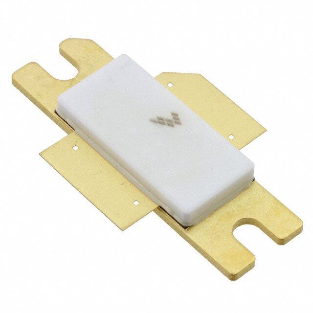
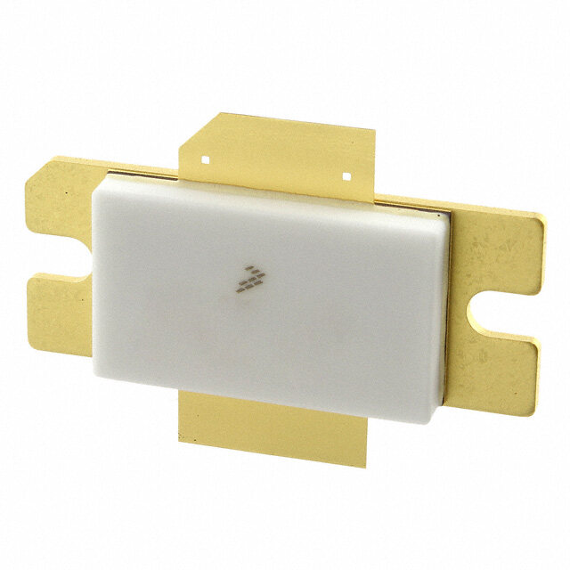
| 描述 | TRANSISTOR RF FET 3.5GHZ PLD-1.5射频JFET晶体管 3.5GHZ 10W GAAS PLD1.5N |
| 产品分类 | RF FET分离式半导体 |
| Id-ContinuousDrainCurrent | 2.9 A |
| Id-连续漏极电流 | 2.9 A |
| 品牌 | Freescale Semiconductor |
| 产品手册 | |
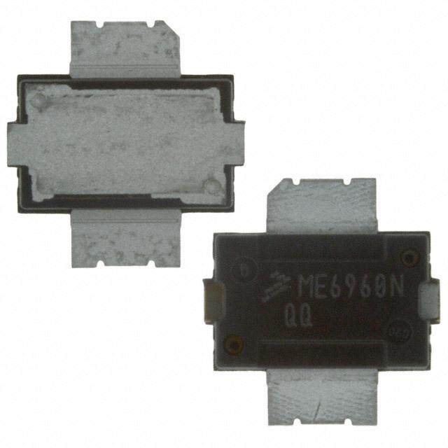
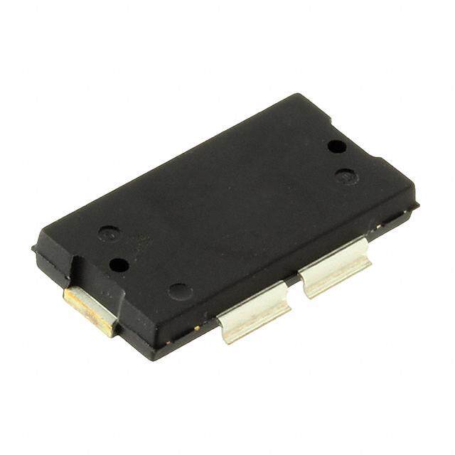
| 产品图片 |
|
| rohs | RoHS 合规性豁免含铅 / 不符合限制有害物质指令(RoHS)规范要求 |
| 产品系列 | 晶体管,晶体管射频,射频JFET晶体管,Freescale Semiconductor MRFG35010ANT1- |
| 数据手册 | |
| P1dB | 9 W |
| 产品型号 | MRFG35010ANT1 |
| PCN封装 | http://cache.freescale.com/files/shared/doc/pcn/PCN15687.htm |
| Vds-Drain-SourceBreakdownVoltage | 15 V |
| Vds-漏源极击穿电压 | 15 V |
| Vgs-Gate-SourceBreakdownVoltage | - 5 V |
| Vgs-栅源极击穿电压 | - 5 V |
| 产品 | RF JFET |
| 产品种类 | 射频JFET晶体管 |
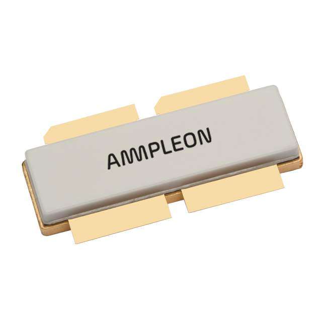
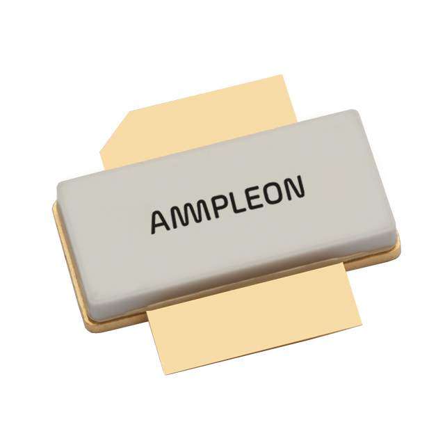
| 供应商器件封装 | PLD-1.5 |
| 其它名称 | MRFG35010ANT1DKR |
| 功率-输出 | 9W |
| 包装 | Digi-Reel® |
| 单位重量 | 280 mg |
| 商标 | Freescale Semiconductor |
| 噪声系数 | - |
| 增益 | 10dB |
| 安装风格 | SMD/SMT |
| 封装 | Reel |
| 封装/外壳 | PLD-1.5 |
| 封装/箱体 | PLD-1.5 |
| 工厂包装数量 | 1000 |
| 技术 | GaAs |
| 晶体管类型 | pHEMT FET |
| 最大工作温度 | + 150 C |
| 标准包装 | 1 |
| 漏极连续电流 | 2.9 A |
| 漏源电压VDS | 15 V |
| 电压-测试 | 12V |
| 电压-额定 | 15V |
| 电流-测试 | 130mA |
| 类型 | GaAs pHEMT |
| 系列 | MRFG35010ANT1 |
| 配置 | Single Dual Source |
| 闸/源击穿电压 | - 5 V |
| 频率 | 3.55GHz |
| 额定电流 | 2.9A |


- 商务部:美国ITC正式对集成电路等产品启动337调查
- 曝三星4nm工艺存在良率问题 高通将骁龙8 Gen1或转产台积电
- 太阳诱电将投资9.5亿元在常州建新厂生产MLCC 预计2023年完工
- 英特尔发布欧洲新工厂建设计划 深化IDM 2.0 战略
- 台积电先进制程称霸业界 有大客户加持明年业绩稳了
- 达到5530亿美元!SIA预计今年全球半导体销售额将创下新高
- 英特尔拟将自动驾驶子公司Mobileye上市 估值或超500亿美元
- 三星加码芯片和SET,合并消费电子和移动部门,撤换高东真等 CEO
- 三星电子宣布重大人事变动 还合并消费电子和移动部门
- 海关总署:前11个月进口集成电路产品价值2.52万亿元 增长14.8%

PDF Datasheet 数据手册内容提取
Freescale Semiconductor DocumentNumber:MRFG35010AN Technical Data Rev.4,8/2013 Gallium Arsenide pHEMT RF Power Field Effect Transistor MRFG35010ANT1 Designedfor WLL/MMDS/BWAor UMTSdriver applications.Characterized from500to5000MHz.DeviceisunmatchedandissuitableforuseinClassAB customerpremiseequipment(CPE)applications. TypicalSingle--CarrierW--CDMAPerformance:VDD=12Vdc,IDQ=130mA, 3.84MHzChannelBandwidth,InputSignalPAR=8.5dB@0.01% 500--5000MHz,9W,12V ProbabilityonCCDF. POWERFET GaAspHEMT Frequency Pout Gps ACPR D IRL (MHz) (W) (dB) (dBc) (%) (dB) 750 1 14.5 --44.0 24.0 --15 2140 1 13.0 --43.0 25.0 --14 2650 1 11.5 --43.0 30.0 --15 Features 9WattsP1dB@3550MHz,CW ExcellentPhaseLinearityandGroupDelayCharacteristics HighEfficiencyandHighLinearity PLD--1.5 PLASTIC InTapeandReel.T1Suffix=1000Units,16mmTapeWidth,13--inchReel. Table1.MaximumRatings Rating Symbol Value Unit Drain--SourceVoltage VDSS 15 Vdc Gate--SourceVoltage VGS --5 Vdc RFInputPower Pin 33 dBm StorageTemperatureRange Tstg --65to+150 C ChannelTemperature(1) Tch 175 C Table2.ThermalCharacteristics Characteristic Symbol Value(2) Unit ThermalResistance,JunctiontoCase RJC 6.5 C/W CaseTemperature77C,1WCW Table3.ESDProtectionCharacteristics TestMethodology Class HumanBodyModel(perJESD22--A114) 2 MachineModel(perEIA/JESD22--A115) A ChargeDeviceModel(perJESD22--C101) IV Table4.MoistureSensitivityLevel TestMethodology Rating PackagePeakTemperature Unit PerJESD22--A113,IPC/JEDECJ--STD--020 3 260 C 1. Forreliableoperation,theoperatingchanneltemperatureshouldnotexceed150C. 2. RefertoAN1955,ThermalMeasurementMethodologyofRFPowerAmplifiers.Gotohttp://www.freescale.com/rf. SelectDocumentation/ApplicationNotes--AN1955. FreescaleSemiconductor,Inc.,2006,2008--2009,2012--2013.Allrightsreserved. MRFG35010ANT1 RFDeviceData FreescaleSemiconductor,Inc. 1
Table5.ElectricalCharacteristics (TA=25Cunlessotherwisenoted) Characteristic Symbol Min Typ Max Unit SaturatedDrainCurrent IDSS — 2.9 — Adc (VDS=3.5Vdc,VGS=0Vdc) OffStateLeakageCurrent IGSS — <1 100 Adc (VGS=--0.4Vdc,VDS=0Vdc) OffStateDrainCurrent IDSO — 0.1 1 mAdc (VDS=12Vdc,VGS=--2.2Vdc) OffStateCurrent IDSX — 2 15 mAdc (VDS=28.5Vdc,VGS=--2.5Vdc) Gate--SourceCut--offVoltage VGS(th) --1.2 --1.0 --0.7 Vdc (VDS=3.5Vdc,IDS=15mA) QuiescentGateVoltage VGS(Q) --1.2 --0.95 --0.7 Vdc (VDS=12Vdc,IDQ=180mA) FunctionalTests(InFreescaleTestFixture,50ohmsystem)VDD=12Vdc,IDQ=130mA,Pout=1WAvg.,f=3550MHz,Single--Carrier W--CDMA,3.84MHzChannelBandwidthCarrier.ACPRmeasuredin3.84MHzChannelBandwidth@5MHzOffset. PAR=8.5dB@0.01%ProbabilityonCCDF. PowerGain Gps 9 10 — dB DrainEfficiency ηD 23 25 — % AdjacentChannelPowerRatio ACPR — --43 --40 dBc TypicalRFPerformance(InFreescaleTestFixture,50hmsystem)VDD=12Vdc,IDQ=130mA,f=3550MHz OutputPower,1dBCompressionPoint,CW P1dB — 9 — W MRFG35010ANT1 RFDeviceData 2 FreescaleSemiconductor,Inc.
C10 C9 C14 C13 C11 C12 C8 C15 C7 C16 C6 C17 C5 C18 C19 C4 R1 C3 C20 C1 C2 C22 C21 MRFG35010AN Rev.6 3500MHz--3600MHz Figure1.MRFG35010ANT1TestCircuitComponentLayout—3550MHz Table6.MRFG35010ANT1TestCircuitComponentDesignationsandValues—3550MHz Part Description PartNumber Manufacturer C1,C21,C22 0.5pFChipCapacitors 08051J0R5BBT AVX C2 0.2pFChipCapacitor 06035J0R2BBT AVX C3 0.5pFChipCapacitor 06035J0R5BBT AVX C4,C19,C20 6.8pFChipCapacitors 08051J6R8BBT AVX C5,C18 10pFChipCapacitors ATC100A100JP150XT ATC C6,C17 100pFChipCapacitors ATC100A101JP150XT ATC C7,C16 100pFChipCapacitors ATC100B101JP500XT ATC C8,C15 1000pFChipCapacitors ATC100B102JP50XT ATC C9,C14 0.1FChipCapacitors CDR33BX104AKWS Kemet C10,C13 39KpFChipCapacitors ATC200B393KP50XT ATC C11,C12 10F,50VChipCapacitors GRM55DR61H106KA88B Murata R1 50ChipResistor P51ETR--ND Newark PCB 0.020,r=3.5 RO4350B Rogers MRFG35010ANT1 RFDeviceData FreescaleSemiconductor,Inc. 3
VGG VDD C11 C10 C9 C8 C7 C6 C5 C18 C17 C16 C15 C14 C13 C12 C4 C19 Z9 Z12 R1 RF RF INPUT OUTPUT Z1 Z2 Z3 Z4 Z5 Z6 Z7 Z8 Z10 Z11 Z13 Z14 Z15 Z16 Z17 C3 C20 C1 C2 C22 C21 Figure2.MRFG35010ANT1TestCircuitSchematic—3550MHz Table7.MRFG35010ANT1TestCircuitMicrostrips—3550MHz Microstrip Description Microstrip Description Z1 0.045x0.689Microstrip Z9 0.025x0.485Microstrip Z2 0.045x0.089Microstrip Z11 0.400x0.215Microstrip Z3 0.020x0.360Microstrip Z12 0.025x0.497Microstrip Z4 0.045x0.029Microstrip Z13 0.025x0.271Microstrip Z5 0.045x0.061Microstrip Z14 0.025x0.363Microstrip Z6 0.045x0.055Microstrip Z15 0.025x0.041Microstrip Z7 0.300x0.125Microstrip Z16 0.045x0.050Microstrip Z8,Z10 0.146x0.070Microstrip Z17 0.045x0.467Microstrip MRFG35010ANT1 RFDeviceData 4 FreescaleSemiconductor,Inc.
TYPICALCHARACTERISTICS—3550MHz 12 50 B) 10 40 (d %) GAIN VDD=12Vdc,IDQ=130mA,f=3550MHz GT CY( CER 8 S3.i8n4glMe--HCzaCrrhiearnWne--lCBDaMndAwidth 30 CIEN RANSDU 6 SL==00..884795----114351..80__ 20 AINEFFI T R G,T 4 10 ,DD D 2 0 10 15 20 25 30 35 40 Pout,OUTPUTPOWER(dBm) Figure3.Single--CarrierW--CDMAPowerGain andDrainEfficiencyversusOutputPower c) --10 --10 B (d VDD=12Vdc,IDQ=130mA,f=3550MHz O Single--CarrierW--CDMA,3.84MHzChannelBandwidth RATI --20 S=0.875--131.0_,L=0.849--145.8_ --15 dB) R S( WE IRL OS O L P --30 --20 N L R E U N T N E A R H --40 --25 T C U T P N N E I DJAC --50 ACPR --30 IRL, A R, P C --60 --35 A 15 20 25 30 35 40 Pout,OUTPUTPOWER(dBm) Figure4.Single--CarrierW--CDMAACPRand InputReturnLossversusOutputPower NOTE:Alldataisreferencedtopackageleadinterface.SandLaretheimpedancespresentedtotheDUT. Alldataisgeneratedfromloadpull,notfromthetestcircuitshown. MRFG35010ANT1 RFDeviceData FreescaleSemiconductor,Inc. 5
TYPICALCHARACTERISTICS—3550MHz 14 60 VDD=12Vdc,IDQ=130mA,f=3550MHz Single--CarrierW--CDMA,3.84MHzChannelBandwidth 12 50 InputSignalPAR=8.5dB@0.01% %) B) Probability(CCDF) Y( RGAIN(d 108 Gps 3400 FFICIENC E E W N G,POps 6 20 ,DRAID 4 D 10 2 0 20 24 28 32 36 40 Pout,OUTPUTPOWER(dBm) Figure5.Single--CarrierW--CDMAPowerGain andDrainEfficiencyversusOutputPower c) --10 --5 B (d VDD=12Vdc,IDQ=140mA,f=3550MHz O Single--CarrierW--CDMA,3.84MHzChannelBandwidth RATI --20 InputSignalPAR=8.5dB@0.01% --10 dB) R Probability(CCDF) S( E S W O O L P --30 --15 N EL IRL UR N T N E A R H --40 --20 T C U T P N N E I DJAC --50 ACPR --25 IRL, A R, P C --60 --30 A 20 25 30 35 40 Pout,OUTPUTPOWER(dBm) Figure6.Single--CarrierW--CDMAACPRand InputReturnLossversusOutputPower NOTE:Dataisgeneratedfromthetestcircuitshown. MRFG35010ANT1 RFDeviceData 6 FreescaleSemiconductor,Inc.
Zo=25 Zload f=3550MHz Zsource f=3550MHz VDD=12Vdc,IDQ=130mA,Pout=1WAvg. f Zsource Zload MHz 3550 4.0--j22.6 4.5--j15.3 Zsource = Testcircuitimpedanceasmeasuredfrom gatetoground. Zload = Testcircuitimpedanceasmeasured fromdraintoground. Input Device Output Matching Under Matching Network Test Network Z Z source load Figure7.SeriesEquivalentSourceandLoadImpedance—3550MHz MRFG35010ANT1 RFDeviceData FreescaleSemiconductor,Inc. 7
--VGG +VDD C8 C7 C12 C11 C9 C6 C13 C10 C5 C14 C4 C15 C3 C16 R1 C1 L1 L2 C19 C20 Q1 C2 R2 C17 C18 C21 MRFG35010ANRev.2 700MHz--900MHz Figure8.MRFG35010ANT1TestCircuitComponentLayout—750MHz Table8.MRFG35010ANT1TestCircuitComponentDesignationsandValues—750MHz Part Description PartNumber Manufacturer C1,C19 100pFChipCapacitors ATC600F101JT250XT ATC C2 10pFChipCapacitor ATC600F100JT250XT ATC C3,C16 10pFChipCapacitors ATC100A100JP150XT ATC C4,C15 100pFChipCapacitors ATC100A101JP150XT ATC C5,C14 100pFChipCapacitors ATC100B101JP500XT ATC C6,C13 1000pFChipCapacitors ATC100B102JP50XT ATC C7,C12 0.1FChipCapacitors CDR33BX104AKWS AVX C8,C11 39KpFChipCapacitors ATC200B393KP500XT ATC C9,C10 22F,35VTantalumCapacitors T491X226K035AT Kemet C17 1.8pFChipCapacitor ATC600F1R8BT250XT ATC C18 6.8pFChipCapacitor ATC600F6R8BT250XT ATC C20 22pFChipCapacitor ATC600F220JT250XT ATC C21 1pFChipCapacitor ATC600F1R0BT250XT ATC L1,L2 18nHChipInductors LL1608--FSL18NJ TOKO Q1 PowerFETGaAsTransistor MRFG35010ANT1 Freescale R1 51,1/10WChipResistor RM73B1JT510J KOASpeer R2 4.7,1/10WChipResistor CR10--4R7J--T Kyocera PCB 0.020,r=3.5 RO4350B Rogers MRFG35010ANT1 RFDeviceData 8 FreescaleSemiconductor,Inc.
VGG + + VDD C9 C8 C7 C6 C5 C14 C13 C12 C11 C10 C4 C15 C3 C16 Z8 R1 Z11 RF L1 L2 RF INPUT C20 OUTPUT Z1 Z2 Z3 Z4 Z5 Z6 Z7 Z9 Z10 Z12 Z13 Z14 Z15 C1 C2 C21 C17 C18 C19 R2 Figure9.MRFG35010ANT1TestCircuitSchematic—750MHz Table9.MRFG35010ANT1TestCircuitMicrostrips—750MHz Microstrip Description Microstrip Description Z1 0.045x0.633Microstrip Z8 0.025x0.155Microstrip Z2 0.045x0.044Microstrip Z10 0.325x0.255Microstrip Z3 0.045x0.422Microstrip Z11 0.025x0.168Microstrip Z4 0.090x0.030Microstrip Z12 0.045x0.080Microstrip Z5 0.110x0.050Microstrip Z13 0.045x0.600Microstrip Z6 0.285x0.200Microstrip Z14 0.045x0.089Microstrip Z7,Z9 0.146x0.070Microstrip Z15 0.045x0.400Microstrip MRFG35010ANT1 RFDeviceData FreescaleSemiconductor,Inc. 9
TYPICALCHARACTERISTICS—750MHz 20 10 VDD=12Vdc,IDQ=130mA,25C VDD=12Vdc,IDQ=130mA,25C 15 B) 5 AIN(dB) 10 LOSS(d 0 G 5 N --5 L R A U GN 0 ET --10 SI R G,SMALL--p --1--50 S11,INPUT ----1250 --15 --25 --20 --30 500 1000 1500 2000 2500 3000 3500 500 1000 1500 2000 2500 3000 3500 f,FREQUENCY(MHz) f,FREQUENCY(MHz) Figure10.Small--SignalGainversusFrequency Figure11.InputReturnLossversusFrequency 10 VDD=12Vdc,IDQ=130mA,25C B) 5 d ( S S 0 O L RN --5 U T RE --10 T U P --15 T U O 2, --20 2 S --25 --30 500 1000 1500 2000 2500 3000 3500 f,FREQUENCY(MHz) Figure12.OutputReturnLossversusFrequency MRFG35010ANT1 RFDeviceData 10 FreescaleSemiconductor,Inc.
TYPICALCHARACTERISTICS—750MHz 18 60 VDD=12Vdc,IDQ=130mA,f=750MHz Single--CarrierW--CDMA,3.84MHzChannelBandwidth 16 50 InputSignalPAR=8.5dB@0.01%Probability(CCDF) %) B) Y( RGAIN(d 1142 Gps 4300 FFICIENC E E W N G,POps10 D 20 ,DRAID 8 10 6 0 20 25 30 35 40 Pout,OUTPUTPOWER(dBm) Figure13.Single--CarrierW--CDMAPowerGain andDrainEfficiencyversusOutputPower c) --10 --5 B (d VDD=12Vdc,IDQ=130mA,f=750MHz O Single--CarrierW--CDMA,3.84MHzChannelBandwidth RATI --20 InputSignalPAR=8.5dB@0.01%Probability(CCDF) --10 dB) R S( E S W O O L P --30 --15 N L R E U NN IRL ET A R H --40 --20 T C U T P N N E ACPR I DJAC --50 --25 IRL, A R, P C --60 --30 A 20 25 30 35 40 Pout,OUTPUTPOWER(dBm) Figure14.Single--CarrierW--CDMAACPRand InputReturnLossversusOutputPower MRFG35010ANT1 RFDeviceData FreescaleSemiconductor,Inc. 11
--VGG +VDD C8 C7 C12 C11 C9 C10 C6 C13 C5 C14 C4 C15 C3 C16 R1 C1 L1 L2 C17 Q1 RFIN C2 RFOUT C18 MRFG35010AN Rev.0 2100MHz--2200MHz Figure15.MRFG35010ANT1TestCircuitComponentLayout—2140MHz Table10.MRFG35010ANT1TestCircuitComponentDesignationsandValues—2140MHz Part Description PartNumber Manufacturer C1 4.7pFChipCapacitor 080514R7BBS AVX C2 0.5pFChipCapacitor 08051J0R5BBS AVX C3,C16 10pFChipCapacitors ATC100A100JP150XT ATC C4,C15 100pFChipCapacitors ATC100A101JP150XT ATC C5,C14 100pFChipCapacitors ATC100B101JP500XT ATC C6,C13 1000pFChipCapacitors ATC100B102JP50XT ATC C7,C12 0.1FChipCapacitors CDR33BX104AKWS AVX C8,C11 39KpFChipCapacitors ATC200B393KP500XT ATC C9,C10 22F,35VTantalumCapacitors T491X226K035AT Kemet C17 15pFChipCapacitor 08051J150GBS AVX C18 1.5pFChipCapacitor 08051J1R5BBS AVX L1 3.9nHInductor LL1608--FH3N9S TOKO L2 8.2nHInductor LL1608--FH8N2S TOKO Q1 PowerFETGaAsTransistor MRFG35010ANT1 Freescale R1 75,1/8WChipResistor ERJ--6GEYJ750V Panasonic PCB 0.020,r=3.5 RO4350B Rogers MRFG35010ANT1 RFDeviceData 12 FreescaleSemiconductor,Inc.
VGG + + VDD C9 C8 C7 C6 C5 C14 C13 C12 C11 C10 C4 C15 C3 C16 R1 Z8 RF L1 L2 RF INPUT OUTPUT Z1 Z2 Z3 Z5 Z6 Z7 Z9 Z10 Z12 Z13 Z14 C1 C2 Z4 C18 Z11 C19 Figure16.MRFG35010ANT1TestCircuitSchematic—2140MHz Table11.MRFG35010ANT1TestCircuitMicrostrips—2140MHz Microstrip Description Microstrip Description Z1,Z14 0.045x0.295Microstrip Z7,Z9 0.146x0.070Microstrip Z2 0.045x0.224Microstrip Z8 0.045x0.098Microstrip Z3 0.045x0.515Microstrip Z10 0.200x0.040Microstrip Z4 0.105x0.045Microstrip Z11 0.260x0.020Microstrip Z5 0.045x0.023Microstrip Z12 0.200x0.632Microstrip Z6 0.450x0.312Microstrip Z13 0.045x0.420Microstrip MRFG35010ANT1 RFDeviceData FreescaleSemiconductor,Inc. 13
TYPICALCHARACTERISTICS—2140MHz 20 10 VDD=12Vdc,IDQ=130mA,25C VDD=12Vdc,IDQ=130mA,25C 15 B) 5 AIN(dB) 10 LOSS(d 0 G 5 N --5 L R A U GN 0 ET --10 SI R G,SMALL--p --1--50 S11,INPUT ----1250 --15 --25 --20 --30 500 1000 1500 2000 2500 3000 3500 500 1000 1500 2000 2500 3000 3500 f,FREQUENCY(MHz) f,FREQUENCY(MHz) Figure17.Small--SignalGainversusFrequency Figure18.InputReturnLossversusFrequency 10 VDD=12Vdc,IDQ=130mA,25C B) 5 d ( S S 0 O L RN --5 U T RE --10 T U P --15 T U O 2, --20 2 S --25 --30 500 1000 1500 2000 2500 3000 3500 f,FREQUENCY(MHz) Figure19.OutputReturnLossversusFrequency MRFG35010ANT1 RFDeviceData 14 FreescaleSemiconductor,Inc.
TYPICALCHARACTERISTICS—2140MHZ 18 60 VDD=12Vdc,IDQ=130mA,f=2140MHz Single--CarrierW--CDMA,3.84MHz 16 50 ChannelBandwidth %) B) InputSignalPAR=8.5dB@0.01% Y( RGAIN(d 1142 Probability(CCDF) Gps 4300 FFICIENC E E W N G,POps10 D 20 ,DRAID 8 10 6 0 20 25 30 35 40 Pout,OUTPUTPOWER(dBm) Figure20.Single--CarrierW--CDMAPowerGain andDrainEfficiencyversusOutputPower c) --10 ----5 B (d VDD=12Vdc,IDQ=140mA,f=2140MHz O Single--CarrierW--CDMA,3.84MHzChannelBandwidth RATI --20 InputSignalPAR=8.5dB@0.01%Probability(CCDF) --10 dB) R S( E S W O O L P --30 --15 N EL IRL UR N T N E A R H --40 --20 T C U T P EN ACPR IN DJAC --50 --25 IRL, A R, P C --60 --30 A 20 25 30 35 40 Pout,OUTPUTPOWER(dBm) Figure21.Single--CarrierW--CDMAACPRand InputReturnLossversusOutputPower MRFG35010ANT1 RFDeviceData FreescaleSemiconductor,Inc. 15
--VGG +VDD C8 C7 C12 C11 C9 C10 C6 C13 C5 C14 C4 C15 C3 C16 R1 C1 C18 L1 L2 C17 C21 Q1 RFIN C2* C19 C20 RFOUT MRFG35010AN Rev.0 2600MHz--2700MHz Note:ComponentnumberC2*islabeledonboardbutnotplaced. Figure22.MRFG35010ANT1TestCircuitComponentLayout—2650MHz Table12.MRFG35010ANT1TestCircuitComponentDesignationsandValues—2650MHz Part Description PartNumber Manufacturer C1 4.7pFChipCapacitor 080514R7BBS AVX C2 ComponentNotPlaced C3,C16 10pFChipCapacitors ATC100A100JP150XT ATC C4,C15 100pFChipCapacitors ATC100A101JP150XT ATC C5,C14 100pFChipCapacitors ATC100B101JP500XT ATC C6,C13 1000pFChipCapacitors ATC100B102JP50XT ATC C7,C12 0.1FChipCapacitors CDR33BX104AKWS AVX C8,C11 39KpFChipCapacitors ATC200B393KP500XT ATC C9,C10 22F,35VTantalumCapacitors T491X226K035AT Kemet C17 15pFChipCapacitor 08051J150GBS AVX C18 0.5pFChipCapacitor 08051J0R5BBS AVX C19 1.5pFChipCapacitor 08051J1R5BBS AVX C20 1pFChipCapacitor 08051J1R0BBS AVX C21 0.4pFChipCapacitor 08051J0R4BBS AVX L1 5.6nHInductor LL1608--FH5N6S TOKO L2 6.8nHInductor LL1608--FH6N8S TOKO Q1 PowerFETGaAsTransistor MRFG35010ANT1 Freescale R1 75,1/8WChipResistor ERJ--6GEYJ750V Panasonic PCB 0.020,r=3.5 RO4350B Rogers MRFG35010ANT1 RFDeviceData 16 FreescaleSemiconductor,Inc.
VGG + + VDD C9 C8 C7 C6 C5 C14 C13 C12 C11 C10 C4 C15 C3 C16 R1 Z9 RF L1 L2 RF INPUT OUTPUT Z1 Z2 Z3 Z4 Z6 Z7 Z8 Z10 Z11 Z13 Z14 Z15 Z16 Z17 C1 C18 C19 Z5 Z12 C20 C17 C21 Figure23.MRFG35010ANT1TestCircuitSchematic—2650MHz Table13.MRFG35010ANT1TestCircuitMicrostrips—2650MHz Microstrip Description Microstrip Description Z1 0.045x0.295Microstrip Z9 0.045x0.098Microstrip Z2 0.045x0.385Microstrip Z11 0.200x0.040Microstrip Z3 0.045x0.077Microstrip Z12 0.260x0.020Microstrip Z4 0.045x0.273Microstrip Z13 0.200x0.632Microstrip Z5 0.105x0.045Microstrip Z14 0.045x0.348Microstrip Z6 0.045x0.023Microstrip Z15 0.045x0.075Microstrip Z7 0.450x0.312Microstrip Z16 0.045x0.150Microstrip Z8,Z10 0.146x0.070Microstrip Z17 0.045x0.152Microstrip MRFG35010ANT1 RFDeviceData FreescaleSemiconductor,Inc. 17
TYPICALCHARACTERISTICS—2650MHz 20 10 VDD=12Vdc,IDQ=130mA,25C VDD=12Vdc,IDQ=130mA,25C 15 B) 5 AIN(dB) 10 LOSS(d 0 G 5 N --5 L R A U GN 0 ET --10 SI R G,SMALL--p --1--50 S11,INPUT ----1250 --15 --25 --20 --30 500 1000 1500 2000 2500 3000 3500 500 1000 1500 2000 2500 3000 3500 f,FREQUENCY(MHz) f,FREQUENCY(MHz) Figure24.Small--SignalGainversusFrequency Figure25.InputReturnLossversusFrequency 10 VDD=12Vdc,IDQ=130mA,25C B) 5 d ( S S 0 O L RN --5 U T RE --10 T U P --15 T U O 2, --20 2 S --25 --30 500 1000 1500 2000 2500 3000 3500 f,FREQUENCY(MHz) Figure26.OutputReturnLossversusFrequency MRFG35010ANT1 RFDeviceData 18 FreescaleSemiconductor,Inc.
TYPICALCHARACTERISTICS—2650MHZ 18 60 VDD=12Vdc,IDQ=130mA,f=2650MHz Single--CarrierW--CDMA 16 50 3.84MHzChannelBandwidth %) B) InputSignalPAR=8.5dB@0.01% Y( RGAIN(d 1142 Probability(CCDF) 4300 FFICIENC E E G,POWps10 Gps D 20 ,DRAIND 8 10 6 0 20 25 30 35 40 Pout,OUTPUTPOWER(dBm) Figure27.Single--CarrierW--CDMAPowerGain andDrainEfficiencyversusOutputPower c) --10 --5 B (d VDD=12Vdc,IDQ=140mA,f=2650MHz O Single--CarrierW--CDMA,3.84MHzChannelBandwidth RATI --20 InputSignalPAR=8.5dB@0.01%Probability(CCDF) --10 dB) R S( E S W O O L P --30 --15 N EL IRL UR N T N E A R H --40 --20 T C U T P N N E I DJAC --50 ACPR --25 IRL, A R, P C --60 --30 A 20 25 30 35 40 Pout,OUTPUTPOWER(dBm) Figure28.Single--CarrierW--CDMAACPRand InputReturnLossversusOutputPower MRFG35010ANT1 RFDeviceData FreescaleSemiconductor,Inc. 19
0.146 3.71 0.095 2.41 0.115 2.92 0.115 2.92 0.020 0.51 inches mm Figure29.PLD--1.5SolderFootprint M10A N B YYWW Figure30.ProductMarking MRFG35010ANT1 RFDeviceData 20 FreescaleSemiconductor,Inc.
PACKAGEDIMENSIONS MRFG35010ANT1 RFDeviceData FreescaleSemiconductor,Inc. 21
MRFG35010ANT1 RFDeviceData 22 FreescaleSemiconductor,Inc.
MRFG35010ANT1 RFDeviceData FreescaleSemiconductor,Inc. 23
PRODUCTDOCUMENTATION,SOFTWAREANDTOOLS Refertothefollowingdocuments,softwareandtoolstoaidyourdesignprocess. ApplicationNotes AN1955:ThermalMeasurementMethodologyofRFPowerAmplifiers Software .s2pFile RFHighPowerModel DevelopmentTools PrintedCircuitBoards ReferenceDesigns W--CDMAReferenceDesignfor2.4--2.5GHz,900mWMRFG35010ANT1Device 725--760MHz,1.0WAVG.,12VLTEAmplifierLineupReferenceDesign ForSoftwareandTools,doaPartNumbersearchathttp://www.freescale.com,andselectthe“PartNumber”link.Gotothe Software&Toolstabonthepart’sProductSummarypagetodownloadtherespectivetool. REVISIONHISTORY Thefollowingtablesummarizesrevisionstothisdocument. Revision Date Description 0 May2006 InitialReleaseofDataSheet 1 Dec.2008 Removed”OperatingCaseTemperatureRange”fromMaximumRatingstablesothatthemaximum channeltemperatureratingisthelimitingthermaldesigncriteriaandnotthecasetemperaturerange,p.1 AddedTable3,ESDProtectionCharacteristics,p.1;renumberedsubsequenttables 2 June2009 ModifieddatasheettoreflectMSLratingchangefrom1to3asaresultofthestandardizationofpacking processasdescribedinProductandProcessChangeNotificationnumber,PCN13516,p.1 3 Dec.2012 AddedTypicalPerformancetable,p.1 Table3,ESDProtectionCharacteristics,removedtheword”Minimum”aftertheESDclassrating.ESD ratingsarecharacterizedduringnewproductdevelopmentbutarenot100%testedduringproduction.ESD ratingsprovidedinthedatasheetareintendedtobeusedasaguidelinewhenhandlingESDsensitive devices,p.1. AddedFigs.8,15and22,TestCircuitComponentLayout—750MHz,2140MHzand2650MHz,and Tables8,10and12,TestCircuitComponentDesignationsandValues —750MHz,2140MHzand 2650MHz,p.8,12and16 AddedFigs.9,16and23,TestCircuitSchematic—750MHz,2140MHzand2650MHz,andTables9,11 and13,TestCircuitMicrostrips—750MHz,2140MHzand2650MHz,p.9,13and17 AddedFigs.10,17and24,Small--SignalGainversusFrequency—750MHz,2140MHzand2650MHz, Figs.11,18and25,InputReturnLossversusFrequency—750MHz,2140MHzand2650MHz,and Figs.12,19and26,OutputReturnLossversusFrequency—750MHz,2140MHzand2650MHz,p.10, 14and18 AddedFigs.13,20and27,Single--CarrierW--CDMAPowerGainandDrainEfficiencyversusOutput Power—750MHz,2140MHzand2650MHz,andFigs.14,21and28,Single--CarrierW--CDMAACPR andInputReturnLossversusOutputPower—750MHz,2140MHzand2650MHz,p.11,15and19 4 Aug.2013 ModifieddatasheettoreflecttapeandreelchangesforPLD--1.5packagedevicesasdescribedinProduct andProcessChangeNotificationnumber,PCN14498,p.1 UpdatedFig.1,MRFG35010ANT1TestCircuitComponentLayout—3550MHz,tocurrenttestcircuit componentlayoutforMRFG35010ANT1part,p.3 MRFG35010ANT1 RFDeviceData 24 FreescaleSemiconductor,Inc.
HowtoReachUs: Informationinthisdocumentisprovidedsolelytoenablesystemandsoftware implementerstouseFreescaleproducts.Therearenoexpressorimpliedcopyright HomePage: licensesgrantedhereundertodesignorfabricateanyintegratedcircuitsbasedonthe freescale.com informationinthisdocument. WebSupport: Freescalereservestherighttomakechangeswithoutfurthernoticetoanyproducts freescale.com/support herein.Freescalemakesnowarranty,representation,orguaranteeregardingthe suitabilityofitsproductsforanyparticularpurpose,nordoesFreescaleassumeany liabilityarisingoutoftheapplicationoruseofanyproductorcircuit,andspecifically disclaimsanyandallliability,includingwithoutlimitationconsequentialorincidental damages.“Typical”parametersthatmaybeprovidedinFreescaledatasheetsand/or specificationscananddovaryindifferentapplications,andactualperformancemay varyovertime.Alloperatingparameters,including“typicals,”mustbevalidatedfor eachcustomerapplicationbycustomer’stechnicalexperts.Freescaledoesnotconvey anylicenseunderitspatentrightsnortherightsofothers.Freescalesellsproducts pursuanttostandardtermsandconditionsofsale,whichcanbefoundatthefollowing address:freescale.com/SalesTermsandConditions. FreescaleandtheFreescalelogoaretrademarksofFreescaleSemiconductor,Inc., Reg.U.S.Pat.&Tm.Off.Allotherproductorservicenamesarethepropertyoftheir respectiveowners. E2006,2008--2009,2012--2013FreescaleSemiconductor,Inc. MRFG35010ANT1 DRoFcuDmeenvticNeumDbaert:aMRFG35010AN RFerve.e4,s8c/a20le13Semiconductor,Inc. 25