ICGOO在线商城 > 分立半导体产品 > 晶体管 - FET,MOSFET - 射频 > CGH40010F
 Datasheet下载
- 型号: CGH40010F
- 制造商: Cree
- 库位|库存: xxxx|xxxx
- 要求:
| 数量阶梯 | 香港交货 | 国内含税 |
| +xxxx | $xxxx | ¥xxxx |
查看当月历史价格
查看今年历史价格
CGH40010F产品简介:
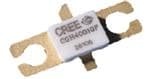
ICGOO电子元器件商城为您提供CGH40010F由Cree设计生产,在icgoo商城现货销售,并且可以通过原厂、代理商等渠道进行代购。 CGH40010F价格参考。CreeCGH40010F封装/规格:晶体管 - FET,MOSFET - 射频, 射频 Mosfet HEMT 28V 200mA 0Hz ~ 6GHz 14.5dB 12.5W 440166。您可以下载CGH40010F参考资料、Datasheet数据手册功能说明书,资料中有CGH40010F 详细功能的应用电路图电压和使用方法及教程。
Cree/Wolfspeed 的 CGH40010F 是一款基于氮化镓(GaN)高电子迁移率晶体管(HEMT)的射频功率MOSFET,广泛应用于高频、高功率场景。其主要应用场景包括:

1. 无线通信基站:适用于4G/LTE和5G宏基站中的射频功率放大器,在2.5–3.8 GHz频段内提供高效、高线性度的信号放大,提升网络覆盖与容量。

2. 雷达系统:凭借高功率密度和优异的热稳定性,常用于军用及民用雷达(如空中交通管制、气象雷达),支持脉冲高功率输出,提高探测距离与精度。

3. 宽带射频放大器:适合工业与广播领域的宽带放大设备,可用于UHF频段的电视广播、公共安全通信等系统。

4. 电子对抗与航空电子:在高可靠性要求的军事电子战系统中,CGH40010F因其耐高温、抗干扰能力强,被用于高功率射频干扰与信号发射模块。

5. 测试与测量设备:作为高性能信号源或功率放大模块,用于研发和生产中的射频器件测试平台。

该器件采用碳化硅衬底的GaN技术,具备高效率、高增益和良好的热导性能,可在较高温度下稳定运行,显著降低冷却需求和系统体积,是现代高频率、高功率射频系统的理想选择。
| 参数 | 数值 |
| 产品目录 | |
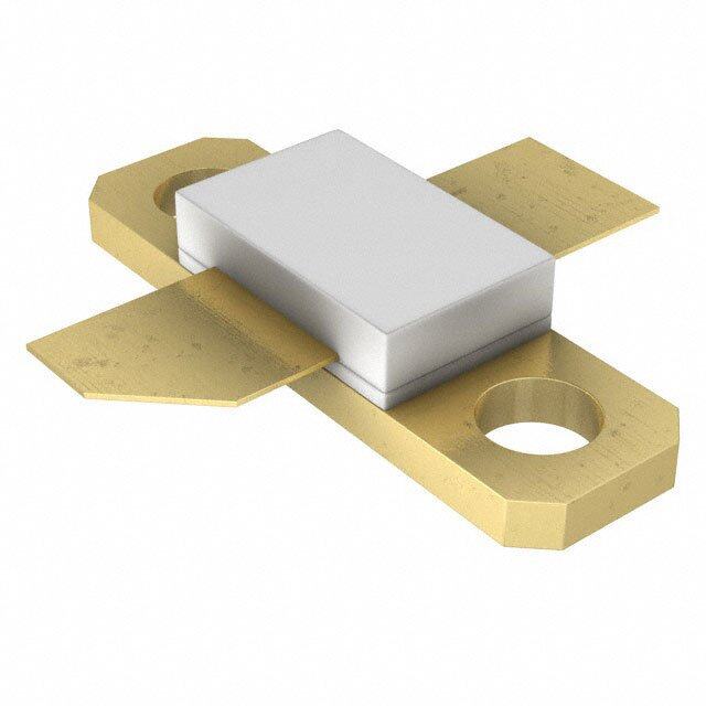
| 描述 | TRANS 10W RF GAN HEMT 440166 PKG |
| 产品分类 | RF FET |
| 品牌 | Cree Inc |
| 数据手册 | |
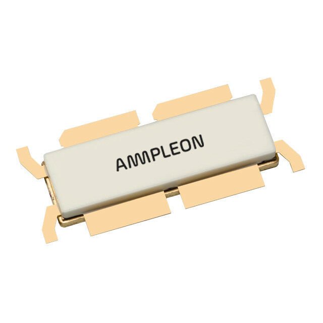
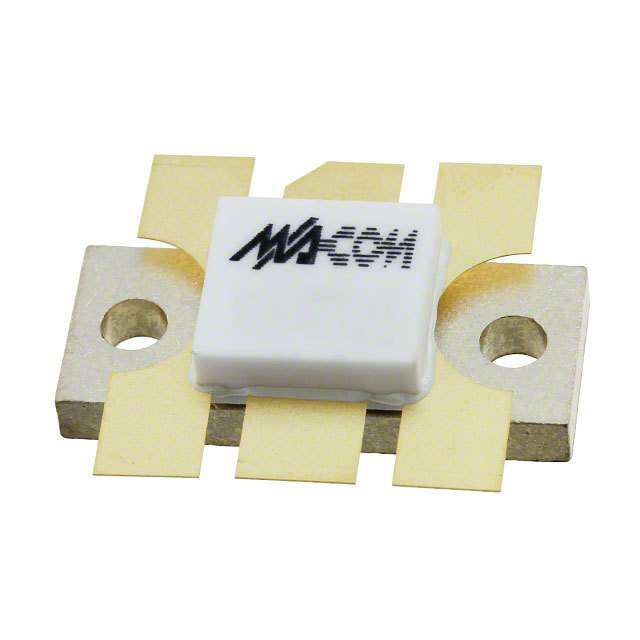
| 产品图片 |
|
| 产品型号 | CGH40010F |
| rohs | 无铅 / 符合限制有害物质指令(RoHS)规范要求 |
| 产品系列 | - |
| 产品目录页面 | |
| 供应商器件封装 | 440166 |
| 其它名称 | CGH40010FE |
| 功率-输出 | 12.5W |
| 包装 | 管件 |
| 噪声系数 | - |
| 增益 | 14.5dB |
| 封装/外壳 | 440166 |
| 晶体管类型 | HEMT |
| 标准包装 | 144 |
| 电压-测试 | 28V |
| 电压-额定 | 84V |
| 电流-测试 | 200mA |
| 配用 | /product-detail/zh/CGH40010F-TB/CGH40010F-TB-ND/1944143 |
| 频率 | 0Hz ~ 6GHz |
| 额定电流 | 3.5A |


- 商务部:美国ITC正式对集成电路等产品启动337调查
- 曝三星4nm工艺存在良率问题 高通将骁龙8 Gen1或转产台积电
- 太阳诱电将投资9.5亿元在常州建新厂生产MLCC 预计2023年完工
- 英特尔发布欧洲新工厂建设计划 深化IDM 2.0 战略
- 台积电先进制程称霸业界 有大客户加持明年业绩稳了
- 达到5530亿美元!SIA预计今年全球半导体销售额将创下新高
- 英特尔拟将自动驾驶子公司Mobileye上市 估值或超500亿美元
- 三星加码芯片和SET,合并消费电子和移动部门,撤换高东真等 CEO
- 三星电子宣布重大人事变动 还合并消费电子和移动部门
- 海关总署:前11个月进口集成电路产品价值2.52万亿元 增长14.8%
PDF Datasheet 数据手册内容提取
CGH40010 10 W, DC - 6 GHz, RF Power GaN HEMT Cree’s CGH40010 is an unmatched, gallium nitride (GaN) high electron mobility transistor (HEMT). The CGH40010, operating from a 28 volt rail, offers a general purpose, broadband solution to a variety of RF and microwave applications. GaN HEMTs offer high efficiency, high gain and wide bandwidth capabilities making the CGH40010 ideal for linear and compressed amplifier circuits. The transistor is available in both screw- down, flange and solder-down, pill packages. PaPcNk’sa:g CeG THyp4e0s0:1 404F0 &1 6C6G, H& 4404001109P6 FEATURES APPLICATIONS • Up to 6 GHz Operation • 2-Way Private Radio • 16 dB Small Signal Gain at 2.0 GHz • Broadband Amplifiers • 14 dB Small Signal Gain at 4.0 GHz • Cellular Infrastructure • 13 W typical P • Test Instrumentation SAT • 65 % Efficiency at P • Class A, AB, Linear amplifiers suitable for SAT • 28 V Operation OFDM, W-CDMA, EDGE, CDMA waveforms 5 1 0 2 y a M – 0 .4 v e R Subject to change without notice. 1 www.cree.com/wireless
Absolute Maximum Ratings (not simultaneous) at 25˚C Case Temperature Parameter Symbol Rating Units Conditions Drain-Source Voltage V 84 Volts 25˚C DSS Gate-to-Source Voltage V -10, +2 Volts 25˚C GS Storage Temperature T -65, +150 ˚C STG Operating Junction Temperature T 225 ˚C J Maximum Forward Gate Current I 4.0 mA 25˚C GMAX Maximum Drain Current1 I 1.5 A 25˚C DMAX Soldering Temperature2 T 245 ˚C S Screw Torque τ 60 in-oz Thermal Resistance, Junction to Case3 R 8.0 ˚C/W 85˚C θJC Case Operating Temperature3,4 T -40, +150 ˚C C Note: 1 Current limit for long term, reliable operation 2 Refer to the Application Note on soldering at www.cree.com/RF/Document-Library 3 Measured for the CGH40010F at P = 14 W. DISS 4 See also, the Power Dissipation De-rating Curve on Page 6. Electrical Characteristics (T = 25˚C) C Characteristics Symbol Min. Typ. Max. Units Conditions DC Characteristics1 Gate Threshold Voltage V -3.8 -3.0 -2.3 V V = 10 V, I = 3.6 mA GS(th) DC DS D Gate Quiescent Voltage V – -2.7 – V V = 28 V, I = 200 mA GS(Q) DC DS D Saturated Drain Current I 2.9 3.5 – A V = 6.0 V, V = 2.0 V DS DS GS Drain-Source Breakdown Voltage V 120 – – V V = -8 V, I = 3.6 mA BR DC GS D RF Characteristics2 (T = 25˚C, F = 3.7 GHz unless otherwise noted) C 0 Small Signal Gain G 12.5 14.5 – dB V = 28 V, I = 200 mA SS DD DQ Power Output3 P 10 12.5 – W V = 28 V, I = 200 mA SAT DD DQ Drain Efficiency4 η 55 65 – % V = 28 V, I = 200 mA, P DD DQ SAT No damage at all phase angles, Output Mismatch Stress VSWR – – 10 : 1 Y V = 28 V, I = 200 mA, DD DQ P = 10 W CW OUT Dynamic Characteristics Input Capacitance C – 4.5 – pF V = 28 V, V = -8 V, f = 1 MHz GS DS gs Output Capacitance C – 1.3 – pF V = 28 V, V = -8 V, f = 1 MHz DS DS gs Feedback Capacitance C – 0.2 – pF V = 28 V, V = -8 V, f = 1 MHz GD DS gs Notes: 1 Measured on wafer prior to packaging. 2 Measured in CGH40010-AMP. 3 P is defined as I = 0.36 mA. SAT G 4 Drain Efficiency = P / P OUT DC Cree, Inc. 4600 Silicon Drive Copyright © 2006-2015 Cree, Inc. All rights reserved. The information in this document is subject to change without notice. Cree and the Cree logo are Durham, North Carolina, USA 27703 registered trademarks of Cree, Inc. USA Tel: +1.919.313.5300 Fax: +1.919.869.2733 2 CGH40010 Rev 4.0 www.cree.com/rf
CGH40010 Nominal Fixture Performance Typical Performance Small Signal Gain and Return Loss vs Frequency of the CGH400S10 p ian rtahem CeGteHr4s0010-AMP 20 3.4 GHz 3.8 GHz 14.9 dB 14.31 dB B) 10 3.6 GHz 3.7 GHz d 14.89 dB 14.7 dB ( s s o L n r 0 u 3.7 GHz t e -7.49 dB R ), B d (-10 n DB(|S(2,1)|) ai Fixture_2_G28V1L2w1_43_42 G 3.4 GHz 3.6 GHz 3.8 GHz DB(|S(1,1)|) -10.65 dB -7.497 dB -8.549 dB Fixture_2_G28V1L2w1_43_42 -20 2.5 3 3.5 4 4.5 Frequency (GHz) P , Gain, and Drain Efficiency vs Frequency of the SPAsTat,Gain,andDrainEfficiencyvsFrequencyofthe CGH40010F in the CGH40010-AMP CGH40010FintheCGH40010-TB V = 28 V, I = 200 mA VDDDD=28V,IDDQQ=200mA 18 80 17 70 Efficiency 16 60 B)B) %)%) dd 15 50 (( (( Gain yy nn cc aiai enen GG 14 40 cici W),W), EffiEffi (( nn PSAT13 PSAT 30 DraiDrai Psat 12 Gain 20 DrainEff 11 10 10 0 3.50 3.55 3.60 3.65 3.70 3.75 3.80 3.85 3.90 Frequency(GHz) Cree, Inc. 4600 Silicon Drive Copyright © 2006-2015 Cree, Inc. All rights reserved. The information in this document is subject to change without notice. Cree and the Cree logo are Durham, North Carolina, USA 27703 registered trademarks of Cree, Inc. USA Tel: +1.919.313.5300 Fax: +1.919.869.2733 3 CGH40010 Rev 4.0 www.cree.com/rf
Typical Performance Swept CW Data of CGH40010F vs. Output Power with Source and Load Impedances Optimized for Drain Efficiency at 2.0 GHz SweptCWDataofCGH40015Fvs.OutputPowerwithSource andLoadImpedVanc e=s O2p8ti mVi,z eIdf o=r D2r0ai0n EmffiAciencyat2.0GHz VDD=D2D8V,IDQ=20D0QmA,Freq=2.0GHz 18 80 70 17 60 16 %) 50 y( c B) en d ci n( 15 40 Effi ai n G ai 30 Dr 14 20 13 10 12 0 26 28 30 32 34 36 38 40 42 Pout(dBm) Swept CW Data of CGH40010F vs. Output Power with Source and Load Impedances Optimized for Drain Efficiency at 3.6 GHz SweptCWDataofCGH40015Fvs.OutputPowerwithSource andLoadImpedVanc e=s O2p8ti mVi,z eIdf o=r D2r0ai0n EmffiAciencyat3.6GHz DD DQ VDD=28V,IDQ=200mA,Freq=3.6GHz 16 80 72 15 64 56 14 %) ( 48 y B) nc d e Gain( 13 40 Effici 32 n ai 12 Dr 24 16 11 8 10 0 23 25 27 29 31 33 35 37 39 41 43 Pout(dBm) Cree, Inc. 4600 Silicon Drive Copyright © 2006-2015 Cree, Inc. All rights reserved. The information in this document is subject to change without notice. Cree and the Cree logo are Durham, North Carolina, USA 27703 registered trademarks of Cree, Inc. USA Tel: +1.919.313.5300 Fax: +1.919.869.2733 4 CGH40010 Rev 4.0 www.cree.com/rf
Typical Performance Swept CW Data of CGH40010F vs. Output Power with Source and Load Impedances Optimized for P1 Power at 3.6 GHz SweptCWDataofCGH40015Fvs.OutputPowerwithSource andLoadImpVeda n=c e2s8O pVt,im Iize d= fo2r0P01 PmowAerat3.6GHz VDD=2D8DV,IDQ=200DQmA,Freq=3.6GHz 14 60 54 13 48 42 12 %) ( 36 y B) nc d e Gain( 11 30 Effici 24 n ai 10 Dr 18 12 9 6 8 0 23 25 27 29 31 33 35 37 39 41 43 Pout(dBm) Simulated Maximum Available Gain and K Factor of the CGH40010F V = 28 V, I = 200 mA DD DQ ) B r o d t ( c G a A F M K Cree, Inc. 4600 Silicon Drive Copyright © 2006-2015 Cree, Inc. All rights reserved. The information in this document is subject to change without notice. Cree and the Cree logo are Durham, North Carolina, USA 27703 registered trademarks of Cree, Inc. USA Tel: +1.919.313.5300 Fax: +1.919.869.2733 5 CGH40010 Rev 4.0 www.cree.com/rf
Typical Noise Performance Simulated Minimum Noise Figure and Noise Resistance vs Frequency of the CGH40010F V = 28 V, I = 100 mA DD DQ ) B d s) e ( m r h u O g ( Fi e e nc ois ta m N esis u R m e Mini Nois Electrostatic Discharge (ESD) Classifications Parameter Symbol Class Test Methodology Human Body Model HBM 1A > 250 V JEDEC JESD22 A114-D Charge Device Model CDM 1 < 200 V JEDEC JESD22 C101-C Cree, Inc. 4600 Silicon Drive Copyright © 2006-2015 Cree, Inc. All rights reserved. The information in this document is subject to change without notice. Cree and the Cree logo are Durham, North Carolina, USA 27703 registered trademarks of Cree, Inc. USA Tel: +1.919.313.5300 Fax: +1.919.869.2733 6 CGH40010 Rev 4.0 www.cree.com/rf
Source and Load Impedances D Z Source Z Load G S Frequency (MHz) Z Source Z Load 500 20.2 + j16.18 51.7 + j15.2 1000 8.38 + j9.46 41.4 + j28.5 1500 7.37 + j0 28.15 + j29 2500 3.19 - j4.76 19 + j9.2 3500 3.18 - j13.3 14.6 + j7.46 Note 1. V = 28V, I = 200mA in the 440166 package. DD DQ Note 2. Optimized for power, gain, P and PAE. SAT Note 3. When using this device at low frequency, series resistors should be used to maintain amplifier stability. CGH40010 Power Dissipation De-rating Curve CGH40010FCWPowerDissipationDe-ratingCurve 16 14 12 W)W) (( nn oo 10 atiati pp sisi DisDis 8 erer Note1 ww oo 6 PP 4 2 0 0 25 50 75 100 125 150 175 200 225 250 MaximumCaseTemperature(°C) Note 1. Area exceeds Maximum Case Operating Temperature (See Page 2). Cree, Inc. 4600 Silicon Drive Copyright © 2006-2015 Cree, Inc. All rights reserved. The information in this document is subject to change without notice. Cree and the Cree logo are Durham, North Carolina, USA 27703 registered trademarks of Cree, Inc. USA Tel: +1.919.313.5300 Fax: +1.919.869.2733 7 CGH40010 Rev 4.0 www.cree.com/rf
CGH40010-AMP Demonstration Amplifier Circuit Bill of Materials Designator Description Qty R1,R2 RES,1/16W,0603,1%,0 OHMS 1 R3 RES,1/16W,0603,1%,47 OHMS 1 R4 RES,1/16W,0603,1%,100 OHMS 1 C6 CAP, 470PF, 5%,100V, 0603 1 C17 CAP, 33 UF, 20%, G CASE 1 C16 CAP, 1.0UF, 100V, 10%, X7R, 1210 1 C8 CAP 10UF 16V TANTALUM 1 C14 CAP, 100.0pF, +/-5%, 0603 1 C1 CAP, 0.5pF, +/-0.05pF, 0603 1 C2 CAP, 0.7pF, +/-0.1pF, 0603 1 C10,C11 CAP, 1.0pF, +/-0.1pF, 0603 2 C4,C12 CAP, 10.0pF,+/-5%, 0603 2 C5,C13 CAP, 39pF, +/-5%, 0603 2 C7,C15 CAP,33000PF, 0805,100V, X7R 2 J3,J4 CONN SMA STR PANEL JACK RECP 1 J2 HEADER RT>PLZ.1CEN LK 2 POS 1 J1 HEADER RT>PLZ .1CEN LK 5POS 1 - PCB, RO4350B, Er = 3.48, h = 20 mil 1 Q1 CGH40010F or CGH40010P 1 CGH40010-AMP Demonstration Amplifier Circuit Cree, Inc. 4600 Silicon Drive Copyright © 2006-2015 Cree, Inc. All rights reserved. The information in this document is subject to change without notice. Cree and the Cree logo are Durham, North Carolina, USA 27703 registered trademarks of Cree, Inc. USA Tel: +1.919.313.5300 Fax: +1.919.869.2733 8 CGH40010 Rev 4.0 www.cree.com/rf
CGH40010-AMP Demonstration Amplifier Circuit Schematic CGH40010-AMP Demonstration Amplifier Circuit Outline Cree, Inc. 4600 Silicon Drive Copyright © 2006-2015 Cree, Inc. All rights reserved. The information in this document is subject to change without notice. Cree and the Cree logo are Durham, North Carolina, USA 27703 registered trademarks of Cree, Inc. USA Tel: +1.919.313.5300 Fax: +1.919.869.2733 9 CGH40010 Rev 4.0 www.cree.com/rf
Typical Package S-Parameters for CGH40010 (Small Signal, V = 28 V, I = 100 mA, angle in degrees) DS DQ Frequency Mag S11 Ang S11 Mag S21 Ang S21 Mag S12 Ang S12 Mag S22 Ang S22 500 MHz 0.909 -123.34 17.19 108.22 0.027 21.36 0.343 -90.81 600 MHz 0.902 -133.06 14.86 101.82 0.028 15.60 0.329 -98.65 700 MHz 0.897 -140.73 13.04 96.45 0.028 10.87 0.321 -104.84 800 MHz 0.894 -146.96 11.58 91.78 0.029 6.84 0.317 -109.84 900 MHz 0.891 -152.16 10.41 87.61 0.029 3.33 0.316 -113.95 1.0 GHz 0.890 -156.60 9.43 83.82 0.029 0.19 0.318 -117.42 1.1 GHz 0.889 -160.47 8.62 80.31 0.029 -2.66 0.321 -120.40 1.2 GHz 0.888 -163.90 7.93 77.02 0.029 -5.28 0.326 -123.02 1.3 GHz 0.887 -166.99 7.34 73.90 0.029 -7.72 0.332 -125.36 1.4 GHz 0.887 -169.80 6.82 70.92 0.029 -10.01 0.338 -127.51 1.5 GHz 0.887 -172.39 6.38 68.05 0.029 -12.18 0.345 -129.50 1.6 GHz 0.887 -174.80 5.98 65.28 0.028 -14.24 0.353 -131.37 1.7 GHz 0.887 -177.07 5.63 62.59 0.028 -16.21 0.360 -133.15 1.8 GHz 0.887 -179.22 5.32 59.97 0.028 -18.09 0.369 -134.87 1.9 GHz 0.887 178.73 5.04 57.41 0.028 -19.91 0.377 -136.54 2.0 GHz 0.888 176.76 4.78 54.89 0.027 -21.66 0.385 -138.17 2.1 GHz 0.888 174.86 4.55 52.42 0.027 -23.35 0.393 -139.77 2.2 GHz 0.888 173.02 4.34 49.99 0.027 -24.98 0.402 -141.34 2.3 GHz 0.888 171.23 4.15 47.60 0.026 -26.56 0.410 -142.90 2.4 GHz 0.889 169.48 3.97 45.24 0.026 -28.08 0.418 -144.45 2.5 GHz 0.889 167.76 3.81 42.90 0.026 -29.55 0.426 -145.99 2.6 GHz 0.890 166.07 3.66 40.59 0.025 -30.98 0.434 -147.53 2.7 GHz 0.890 164.39 3.53 38.30 0.025 -32.36 0.442 -149.06 2.8 GHz 0.890 162.74 3.40 36.03 0.025 -33.69 0.450 -150.59 2.9 GHz 0.891 161.10 3.28 33.78 0.024 -34.97 0.458 -152.12 3.0 GHz 0.891 159.46 3.17 31.55 0.024 -36.20 0.465 -153.65 3.2 GHz 0.892 156.21 2.97 27.12 0.023 -38.51 0.479 -156.72 3.4 GHz 0.893 152.96 2.79 22.73 0.022 -40.63 0.493 -159.80 3.6 GHz 0.893 149.69 2.64 18.38 0.022 -42.52 0.505 -162.90 3.8 GHz 0.894 146.38 2.50 14.05 0.021 -44.17 0.517 -166.03 4.0 GHz 0.894 143.03 2.38 9.72 0.020 -45.56 0.527 -169.19 4.2 GHz 0.894 139.61 2.28 5.40 0.019 -46.67 0.537 -172.39 4.4 GHz 0.895 136.11 2.18 1.07 0.019 -47.46 0.546 -175.64 4.6 GHz 0.895 132.53 2.09 -3.29 0.018 -47.90 0.554 -178.95 4.8 GHz 0.895 128.85 2.01 -7.68 0.017 -47.96 0.561 177.69 5.0 GHz 0.895 125.06 1.94 -12.10 0.017 -47.61 0.568 174.25 5.2 GHz 0.895 121.15 1.88 -16.58 0.016 -46.84 0.573 170.72 5.4 GHz 0.895 117.11 1.82 -21.12 0.016 -45.67 0.578 167.10 5.6 GHz 0.895 112.94 1.77 -25.73 0.015 -44.12 0.582 163.38 5.8 GHz 0.895 108.62 1.72 -30.42 0.015 -42.30 0.586 159.54 6.0 GHz 0.895 104.15 1.68 -35.20 0.015 -40.33 0.589 155.56 To download the s-parameters in s2p format, go to the CGH40010 Product page and click on the documentation tab. Cree, Inc. 4600 Silicon Drive Copyright © 2006-2015 Cree, Inc. All rights reserved. The information in this document is subject to change without notice. Cree and the Cree logo are Durham, North Carolina, USA 27703 registered trademarks of Cree, Inc. USA Tel: +1.919.313.5300 Fax: +1.919.869.2733 10 CGH40010 Rev 4.0 www.cree.com/rf
Typical Package S-Parameters for CGH40010 (Small Signal, V = 28 V, I = 200 mA, angle in degrees) DS DQ Frequency Mag S11 Ang S11 Mag S21 Ang S21 Mag S12 Ang S12 Mag S22 Ang S22 500 MHz 0.911 -130.62 18.41 105.41 0.022 19.44 0.303 -112.24 600 MHz 0.906 -139.65 15.80 99.47 0.023 14.31 0.299 -119.83 700 MHz 0.902 -146.70 13.80 94.50 0.023 10.17 0.298 -125.50 800 MHz 0.899 -152.41 12.22 90.19 0.023 6.68 0.299 -129.85 900 MHz 0.898 -157.17 10.96 86.34 0.024 3.67 0.302 -133.28 1.0 GHz 0.896 -161.24 9.92 82.82 0.024 0.99 0.305 -136.05 1.1 GHz 0.896 -164.79 9.06 79.56 0.024 -1.41 0.309 -138.34 1.2 GHz 0.895 -167.95 8.33 76.49 0.024 -3.62 0.314 -140.30 1.3 GHz 0.895 -170.80 7.70 73.57 0.023 -5.66 0.320 -142.01 1.4 GHz 0.894 -173.41 7.17 70.78 0.023 -7.56 0.326 -143.54 1.5 GHz 0.894 -175.82 6.70 68.08 0.023 -9.35 0.332 -144.94 1.6 GHz 0.894 -178.09 6.28 65.47 0.023 -11.05 0.338 -146.24 1.7 GHz 0.894 179.78 5.92 62.92 0.023 -12.66 0.345 -147.48 1.8 GHz 0.894 177.75 5.59 60.43 0.023 -14.19 0.352 -148.68 1.9 GHz 0.894 175.81 5.30 57.99 0.023 -15.65 0.358 -149.84 2.0 GHz 0.894 173.94 5.04 55.59 0.022 -17.05 0.365 -150.99 2.1 GHz 0.894 172.13 4.80 53.23 0.022 -18.39 0.372 -152.12 2.2 GHz 0.894 170.37 4.58 50.91 0.022 -19.67 0.379 -153.26 2.3 GHz 0.895 168.65 4.38 48.61 0.022 -20.90 0.386 -154.39 2.4 GHz 0.895 166.96 4.20 46.33 0.021 -22.08 0.393 -155.54 2.5 GHz 0.895 165.30 4.03 44.08 0.021 -23.20 0.400 -156.69 2.6 GHz 0.895 163.66 3.88 41.84 0.021 -24.27 0.407 -157.85 2.7 GHz 0.895 162.04 3.74 39.63 0.021 -25.28 0.414 -159.03 2.8 GHz 0.895 160.43 3.60 37.43 0.020 -26.25 0.420 -160.22 2.9 GHz 0.896 158.83 3.48 35.24 0.020 -27.16 0.427 -161.42 3.0 GHz 0.896 157.24 3.37 33.06 0.020 -28.02 0.433 -162.64 3.2 GHz 0.896 154.06 3.16 28.74 0.019 -29.57 0.446 -165.13 3.4 GHz 0.896 150.87 2.98 24.44 0.019 -30.88 0.457 -167.69 3.6 GHz 0.896 147.66 2.82 20.16 0.018 -31.95 0.468 -170.31 3.8 GHz 0.897 144.41 2.68 15.89 0.018 -32.76 0.478 -173.00 4.0 GHz 0.897 141.10 2.56 11.61 0.017 -33.30 0.488 -175.77 4.2 GHz 0.897 137.72 2.45 7.33 0.017 -33.55 0.497 -178.61 4.4 GHz 0.897 134.26 2.35 3.03 0.017 -33.50 0.505 178.47 4.6 GHz 0.897 130.71 2.26 -1.31 0.016 -33.18 0.512 175.46 4.8 GHz 0.896 127.06 2.17 -5.68 0.016 -32.58 0.518 172.36 5.0 GHz 0.896 123.30 2.10 -10.09 0.016 -31.74 0.524 169.16 5.2 GHz 0.896 119.42 2.04 -14.57 0.016 -30.72 0.529 165.86 5.4 GHz 0.896 115.41 1.98 -19.10 0.016 -29.60 0.534 162.44 5.6 GHz 0.896 111.26 1.92 -23.71 0.016 -28.46 0.537 158.89 5.8 GHz 0.895 106.97 1.87 -28.40 0.017 -27.41 0.540 155.20 6.0 GHz 0.895 102.53 1.82 -33.19 0.017 -26.54 0.543 151.36 To download the s-parameters in s2p format, go to the CGH40010 Product Page and click on the documentation tab. Cree, Inc. 4600 Silicon Drive Copyright © 2006-2015 Cree, Inc. All rights reserved. The information in this document is subject to change without notice. Cree and the Cree logo are Durham, North Carolina, USA 27703 registered trademarks of Cree, Inc. USA Tel: +1.919.313.5300 Fax: +1.919.869.2733 11 CGH40010 Rev 4.0 www.cree.com/rf
Typical Package S-Parameters for CGH40010 (Small Signal, V = 28 V, I = 500 mA, angle in degrees) DS DQ Frequency Mag S11 Ang S11 Mag S21 Ang S21 Mag S12 Ang S12 Mag S22 Ang S22 500 MHz 0.914 -135.02 18.58 103.70 0.020 18.36 0.300 -126.80 600 MHz 0.909 -143.57 15.88 98.05 0.020 13.67 0.302 -133.51 700 MHz 0.906 -150.23 13.83 93.33 0.021 9.90 0.304 -138.40 800 MHz 0.904 -155.61 12.23 89.23 0.021 6.77 0.307 -142.08 900 MHz 0.903 -160.09 10.95 85.56 0.021 4.08 0.311 -144.94 1.0 GHz 0.902 -163.93 9.91 82.21 0.021 1.71 0.314 -147.23 1.1 GHz 0.901 -167.29 9.04 79.09 0.021 -0.41 0.319 -149.10 1.2 GHz 0.901 -170.29 8.31 76.15 0.021 -2.35 0.323 -150.69 1.3 GHz 0.900 -173.00 7.69 73.35 0.021 -4.12 0.328 -152.07 1.4 GHz 0.900 -175.50 7.15 70.66 0.021 -5.78 0.333 -153.29 1.5 GHz 0.900 -177.81 6.69 68.07 0.021 -7.32 0.338 -154.41 1.6 GHz 0.900 -179.98 6.27 65.54 0.021 -8.77 0.344 -155.44 1.7 GHz 0.900 177.96 5.91 63.08 0.020 -10.15 0.349 -156.43 1.8 GHz 0.899 176.00 5.59 60.67 0.020 -11.45 0.355 -157.38 1.9 GHz 0.899 174.12 5.30 58.30 0.020 -12.68 0.361 -158.30 2.0 GHz 0.899 172.31 5.04 55.97 0.020 -13.85 0.366 -159.22 2.1 GHz 0.899 170.54 4.80 53.67 0.020 -14.96 0.372 -160.14 2.2 GHz 0.900 168.83 4.58 51.40 0.020 -16.01 0.378 -161.06 2.3 GHz 0.900 167.15 4.39 49.16 0.019 -17.01 0.384 -161.99 2.4 GHz 0.900 165.49 4.21 46.94 0.019 -17.95 0.390 -162.93 2.5 GHz 0.900 163.87 4.04 44.73 0.019 -18.85 0.396 -163.88 2.6 GHz 0.900 162.26 3.89 42.54 0.019 -19.69 0.402 -164.86 2.7 GHz 0.900 160.66 3.75 40.37 0.019 -20.48 0.407 -165.85 2.8 GHz 0.900 159.08 3.62 38.21 0.019 -21.21 0.413 -166.86 2.9 GHz 0.900 157.51 3.50 36.05 0.018 -21.89 0.418 -167.89 3.0 GHz 0.900 155.93 3.39 33.91 0.018 -22.52 0.424 -168.95 3.2 GHz 0.900 152.79 3.18 29.65 0.018 -23.61 0.435 -171.12 3.4 GHz 0.900 149.64 3.00 25.40 0.017 -24.48 0.445 -173.38 3.6 GHz 0.900 146.45 2.85 21.17 0.017 -25.11 0.454 -175.73 3.8 GHz 0.900 143.23 2.71 16.93 0.017 -25.51 0.463 -178.17 4.0 GHz 0.900 139.94 2.58 12.69 0.017 -25.67 0.471 179.30 4.2 GHz 0.900 136.58 2.47 8.43 0.016 -25.60 0.479 176.67 4.4 GHz 0.899 133.14 2.38 4.15 0.016 -25.32 0.486 173.94 4.6 GHz 0.899 129.61 2.29 -0.17 0.016 -24.85 0.492 171.12 4.8 GHz 0.899 125.97 2.21 -4.53 0.016 -24.24 0.498 168.18 5.0 GHz 0.898 122.23 2.13 -8.94 0.016 -23.54 0.503 165.13 5.2 GHz 0.898 118.36 2.07 -13.41 0.016 -22.80 0.507 161.96 5.4 GHz 0.898 114.36 2.01 -17.95 0.017 -22.11 0.511 158.66 5.6 GHz 0.897 110.22 1.95 -22.56 0.017 -21.54 0.514 155.22 5.8 GHz 0.897 105.94 1.90 -27.26 0.018 -21.16 0.517 151.63 6.0 GHz 0.897 101.51 1.86 -32.04 0.019 -21.04 0.519 147.87 To download the s-parameters in s2p format, go to the CGH40010 Product Page and click on the documentation tab. Cree, Inc. 4600 Silicon Drive Copyright © 2006-2015 Cree, Inc. All rights reserved. The information in this document is subject to change without notice. Cree and the Cree logo are Durham, North Carolina, USA 27703 registered trademarks of Cree, Inc. USA Tel: +1.919.313.5300 Fax: +1.919.869.2733 12 CGH40010 Rev 4.0 www.cree.com/rf
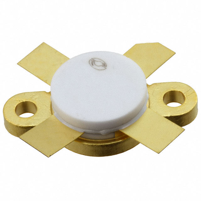
Product Dimensions CGH40010F (Package Type — 440166) Product Dimensions CGH40010P (Package Type — 440196) Cree, Inc. 4600 Silicon Drive Copyright © 2006-2015 Cree, Inc. All rights reserved. The information in this document is subject to change without notice. Cree and the Cree logo are Durham, North Carolina, USA 27703 registered trademarks of Cree, Inc. USA Tel: +1.919.313.5300 Fax: +1.919.869.2733 13 CGH40010 Rev 4.0 www.cree.com/rf
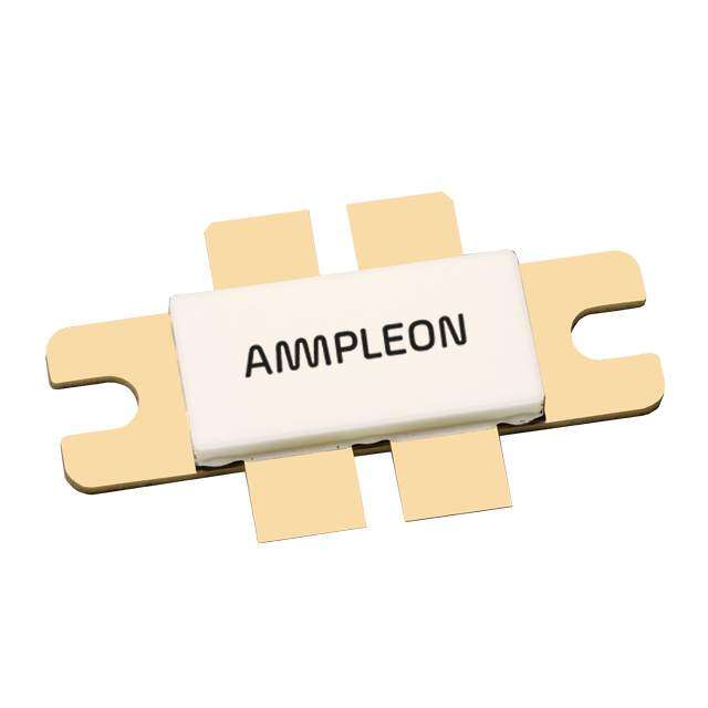
Product Ordering Information Order Number Description Unit of Measure Image CGH40010F GaN HEMT Each CGH40010P GaN HEMT Each CGH40010F-TB Test board without GaN HEMT Each CGH40010F-AMP Test board with GaN HEMT installed Each Cree, Inc. 4600 Silicon Drive Copyright © 2006-2015 Cree, Inc. All rights reserved. The information in this document is subject to change without notice. Cree and the Cree logo are Durham, North Carolina, USA 27703 registered trademarks of Cree, Inc. USA Tel: +1.919.313.5300 Fax: +1.919.869.2733 14 CGH40010 Rev 4.0 www.cree.com/rf
Disclaimer Specifications are subject to change without notice. Cree, Inc. believes the information contained within this data sheet to be accurate and reliable. However, no responsibility is assumed by Cree for any infringement of patents or other rights of third parties which may result from its use. No license is granted by implication or otherwise under any patent or patent rights of Cree. Cree makes no warranty, representation or guarantee regarding the suitability of its products for any particular purpose. “Typical” parameters are the average values expected by Cree in large quantities and are provided for information purposes only. These values can and do vary in different applications and actual performance can vary over time. All operating parameters should be validated by customer’s technical experts for each application. Cree products are not designed, intended or authorized for use as components in applications intended for surgical implant into the body or to support or sustain life, in applications in which the failure of the Cree product could result in personal injury or death or in applications for planning, construction, maintenance or direct operation of a nuclear facility. For more information, please contact: Cree, Inc. 4600 Silicon Drive Durham, North Carolina, USA 27703 www.cree.com/RF Sarah Miller Marketing Cree, RF Components 1.919.407.5302 Ryan Baker Marketing & Sales Cree, RF Components 1.919.407.7816 Tom Dekker Sales Director Cree, RF Components 1.919.407.5639 Cree, Inc. 4600 Silicon Drive Copyright © 2006-2015 Cree, Inc. All rights reserved. The information in this document is subject to change without notice. Cree and the Cree logo are Durham, North Carolina, USA 27703 registered trademarks of Cree, Inc. USA Tel: +1.919.313.5300 Fax: +1.919.869.2733 15 CGH40010 Rev 4.0 www.cree.com/rf
Mouser Electronics Authorized Distributor Click to View Pricing, Inventory, Delivery & Lifecycle Information: C ree, Inc.: CGH40010F CGH40010F-TB