ICGOO在线商城 > 分立半导体产品 > 晶体管 - FET,MOSFET - 射频 > MRF6V2300NBR1
 Datasheet下载
- 型号: MRF6V2300NBR1
- 制造商: Freescale Semiconductor
- 库位|库存: xxxx|xxxx
- 要求:
| 数量阶梯 | 香港交货 | 国内含税 |
| +xxxx | $xxxx | ¥xxxx |
查看当月历史价格
查看今年历史价格
MRF6V2300NBR1产品简介:
ICGOO电子元器件商城为您提供MRF6V2300NBR1由Freescale Semiconductor设计生产,在icgoo商城现货销售,并且可以通过原厂、代理商等渠道进行代购。 MRF6V2300NBR1价格参考。Freescale SemiconductorMRF6V2300NBR1封装/规格:晶体管 - FET,MOSFET - 射频, RF Mosfet LDMOS 50V 900mA 220MHz 25.5dB 300W TO-272 WB-4。您可以下载MRF6V2300NBR1参考资料、Datasheet数据手册功能说明书,资料中有MRF6V2300NBR1 详细功能的应用电路图电压和使用方法及教程。
NXP USA Inc. 的 MRF6V2300NBR1 是一款高功率射频MOSFET晶体管,属于射频功率放大器器件,广泛应用于需要高效率和高稳定性的射频系统中。其主要应用场景包括:

1. 工业、科学和医疗(ISM)频段设备:该器件支持在225–240 MHz频段高效工作,适用于ISM频段的射频能量应用,如射频加热、塑料焊接、介质加热等工业加热与处理系统。

2. 广播发射系统:MRF6V2300NBR1具备高输出功率能力(可达300W),适合用于FM广播或电视发射机中的末级功率放大,提供稳定的信号放大性能。

3. 陆地移动通信基站:在公共安全通信、消防、警察及交通运输等领域的VHF/UHF频段基站中,该器件可用于构建高可靠性功率放大模块,确保远距离清晰通信。

4. 航空与国防雷达系统:凭借其高耐用性和在恶劣环境下的稳定性,适用于某些地面雷达和通信系统的射频放大单元。

该器件采用先进的LDMOS技术,具有高增益、良好的热稳定性和出色的抗负载失配能力,适合连续波(CW)和调制信号操作。其坚固的封装形式(镍钯金镀层)增强了防潮和可靠性,特别适合长时间高负荷运行的工业和通信设备。总之,MRF6V2300NBR1是一款面向高性能模拟射频放大需求的关键元器件,广泛服务于工业加热、广播传输和专业无线通信领域。
| 参数 | 数值 |
| 产品目录 | |
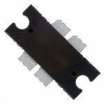
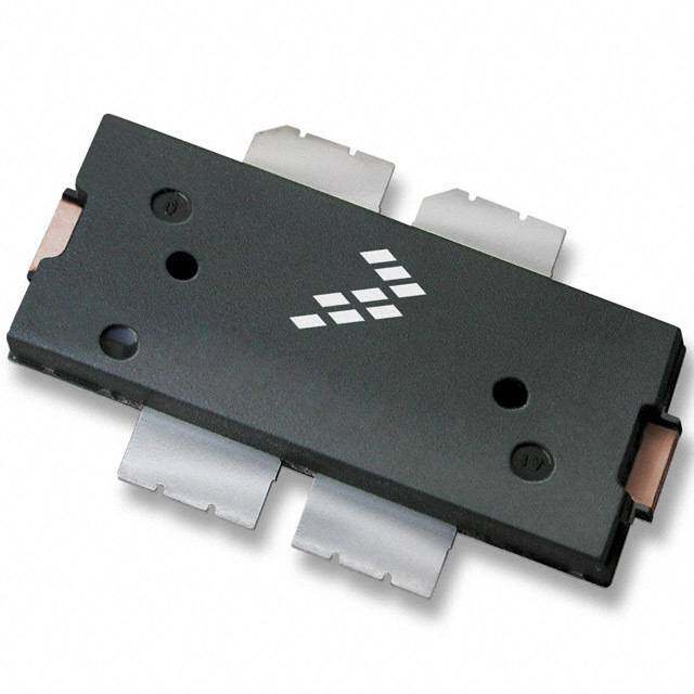
| 描述 | MOSFET RF N-CH TO-272-4 |
| 产品分类 | RF FET |
| 品牌 | Freescale Semiconductor |
| 数据手册 | |
| 产品图片 |
|
| 产品型号 | MRF6V2300NBR1 |
| rohs | 含铅 / 不符合限制有害物质指令(RoHS)规范要求 |
| 产品系列 | - |
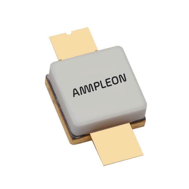
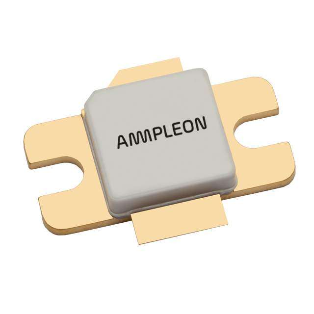
| 供应商器件封装 | TO-272 WB-4 |
| 其它名称 | MRF6V2300NBR1CT |
| 功率-输出 | 300W |
| 包装 | 剪切带 (CT) |
| 噪声系数 | - |
| 增益 | 25.5dB |
| 封装/外壳 | TO-272BB |
| 晶体管类型 | LDMOS |
| 标准包装 | 1 |
| 电压-测试 | 50V |
| 电压-额定 | 110V |
| 电流-测试 | 900mA |
| 频率 | 220MHz |
| 额定电流 | 2.5mA |


- 商务部:美国ITC正式对集成电路等产品启动337调查
- 曝三星4nm工艺存在良率问题 高通将骁龙8 Gen1或转产台积电
- 太阳诱电将投资9.5亿元在常州建新厂生产MLCC 预计2023年完工
- 英特尔发布欧洲新工厂建设计划 深化IDM 2.0 战略
- 台积电先进制程称霸业界 有大客户加持明年业绩稳了
- 达到5530亿美元!SIA预计今年全球半导体销售额将创下新高
- 英特尔拟将自动驾驶子公司Mobileye上市 估值或超500亿美元
- 三星加码芯片和SET,合并消费电子和移动部门,撤换高东真等 CEO
- 三星电子宣布重大人事变动 还合并消费电子和移动部门
- 海关总署:前11个月进口集成电路产品价值2.52万亿元 增长14.8%


PDF Datasheet 数据手册内容提取
Freescale Semiconductor DocumentNumber:MRF6V2300N Technical Data Rev.5,4/2010 RF Power Field Effect Transistors N--Channel Enhancement--Mode Lateral MOSFETs MRF6V2300NR1 DesignedprimarilyforCWlarge--signaloutputanddriverapplicationswith MRF6V2300NBR1 frequenciesupto600MHz.Devicesareunmatchedandaresuitableforusein industrial,medicalandscientificapplications. • TypicalCWPerformance:VDD=50Volts,IDQ=900mA, P =300Watts,f=220MHz 10--600MHz,300W,50V out PowerGain(cid:151)25.5dB LATERALN--CHANNEL DrainEfficiency(cid:151)68% SINGLE--ENDED BROADBAND • CapableofHandling10:1VSWR,@50Vdc,220MHz,300WattsCW RFPOWERMOSFETs OutputPower Features • CharacterizedwithSeriesEquivalentLarge--SignalImpedanceParameters CASE1486--03,STYLE1 • QualifiedUptoaMaximumof50VDDOperation TO--270WB--4 PLASTIC • IntegratedESDProtection MRF6V2300NR1 • 225°CCapablePlasticPackage • RoHSCompliant • InTapeandReel.R1Suffix=500Unitsper44mm,13inchReel. CASE1484--04,STYLE1 TO--272WB--4 PLASTIC MRF6V2300NBR1 PARTSARESINGLE--ENDED Table1.MaximumRatings Rating Symbol Value Unit Drain--SourceVoltage VDSS --0.5,+110 Vdc RFin/VGS RFout/VDS Gate--SourceVoltage VGS --0.5,+10 Vdc StorageTemperatureRange Tstg --65to+150 °C RFin/VGS RFout/VDS CaseOperatingTemperature TC 150 °C OperatingJunctionTemperature(1,2) TJ 225 °C Table2.ThermalCharacteristics (TopView) Characteristic Symbol Value(2,3) Unit Note: Exposedbacksideofthepackageis thesourceterminalforthetransistor. ThermalResistance,JunctiontoCase Figure1.PinConnections CaseTemperature83°C,300WCW RθJC 0.24 °C/W Table3.ESDProtectionCharacteristics TestMethodology Class HumanBodyModel(perJESD22--A114) 2(Minimum) MachineModel(perEIA/JESD22--A115) A(Minimum) ChargeDeviceModel(perJESD22--C101) IV(Minimum) 1. ContinuoususeatmaximumtemperaturewillaffectMTTF. 2. MTTFcalculatoravailableathttp://www.freescale.com/rf.SelectSoftware&Tools/DevelopmentTools/Calculatorstoaccess MTTFcalculatorsbyproduct. 3. RefertoAN1955,ThermalMeasurementMethodologyofRFPowerAmplifiers.Gotohttp://www.freescale.com/rf. SelectDocumentation/ApplicationNotes--AN1955. ©FreescaleSemiconductor,Inc.,2007--2008,2010.Allrightsreserved. MRF6V2300NR1MRF6V2300NBR1 RFDeviceData FreescaleSemiconductor 1
Table4.MoistureSensitivityLevel TestMethodology Rating PackagePeakTemperature Unit PerJESD22--A113,IPC/JEDECJ--STD--020 3 260 °C Table5.ElectricalCharacteristics (TA=25°Cunlessotherwisenoted) Characteristic Symbol Min Typ Max Unit OffCharacteristics ZeroGateVoltageDrainLeakageCurrent IDSS (cid:151) (cid:151) 2.5 mA (VDS=100Vdc,VGS=0Vdc) ZeroGateVoltageDrainLeakageCurrent IDSS (cid:151) (cid:151) 50 μAdc (VDS=50Vdc,VGS=0Vdc) Drain--SourceBreakdownVoltage V(BR)DSS 110 (cid:151) (cid:151) Vdc (ID=150mA,VGS=0Vdc) Gate--SourceLeakageCurrent IGSS (cid:151) (cid:151) 10 μAdc (VGS=5Vdc,VDS=0Vdc) OnCharacteristics GateThresholdVoltage VGS(th) 1 1.63 3 Vdc (VDS=10Vdc,ID=800μAdc) GateQuiescentVoltage VGS(Q) 1.5 2.6 3.5 Vdc (VDD=50Vdc,ID=900mAdc,MeasuredinFunctionalTest) Drain--SourceOn--Voltage VDS(on) (cid:151) 0.28 (cid:151) Vdc (VGS=10Vdc,ID=2Adc) DynamicCharacteristics ReverseTransferCapacitance Crss (cid:151) 2.88 (cid:151) pF (VDS=50Vdc±30mV(rms)ac@1MHz,VGS=0Vdc) OutputCapacitance Coss (cid:151) 120 (cid:151) pF (VDS=50Vdc±30mV(rms)ac@1MHz,VGS=0Vdc) InputCapacitance Ciss (cid:151) 268 (cid:151) pF (VDS=50Vdc,VGS=0Vdc±30mV(rms)ac@1MHz) FunctionalTests(InFreescaleTestFixture,50ohmsystem)VDD=50Vdc,IDQ=900mA,Pout=300W,f=220MHz,CW PowerGain Gps 24 25.5 27 dB DrainEfficiency ηD 66 68 (cid:151) % InputReturnLoss IRL (cid:151) --16 --9 dB TypicalPerformances(InFreescale27MHzand450MHzTestFixtures,50ohmsystem)VDD=50Vdc,IDQ=900mA,Pout=300WCW PowerGain f=27MHz Gps (cid:151) 31.4 (cid:151) dB f=450MHz (cid:151) 21.7 (cid:151) DrainEfficiency f=27MHz ηD (cid:151) 61.5 (cid:151) % f=450MHz (cid:151) 59.1 (cid:151) InputReturnLoss f=27MHz IRL (cid:151) --17.4 (cid:151) dB f=450MHz (cid:151) --24.4 (cid:151) ATTENTION:TheMRF6V2300NandMRF6V2300NBarehighpowerdevicesandspecialconsiderations mustbefollowedinboarddesignandmounting.Incorrectmountingcanleadtointernaltemperatureswhich exceedthemaximumallowableoperatingjunctiontemperature.RefertoFreescaleApplicationNoteAN3263 (forboltdownmounting)orAN1907(forsolderreflowmounting)PRIORTOSTARTINGSYSTEMDESIGNto ensurepropermountingofthesedevices. MRF6V2300NR1MRF6V2300NBR1 RFDeviceData 2 FreescaleSemiconductor
B3 VSUPPLY B1 + VBIAS L2 C17 C18 C19 C20 + + + R1 B2 C1 C2 C3 C4 C5 C6 C7 C14 C15 C16 L1 RF C8 C9 C10 C11 R2 R3 OUTPUT Z7 Z8 Z9 Z10 Z11 RF INPUT Z1 Z2 Z3 Z4 Z5 Z6 C23 C21 C22 C12 DUT C13 Z1 0.352″x0.082″Microstrip Z8 0.085″x0.170″Microstrip Z2 1.567″x0.082″Microstrip Z9 2.275″x0.170″Microstrip Z3 0.857″x0.082″Microstrip Z10 0.945″x0.170″Microstrip Z4 0.276″x0.220″Microstrip Z11 0.443″x0.082″Microstrip Z5 0.434″x0.220″Microstrip PCB ArlonCuClad250GX--0300--55--22,0.030″,εr=2.55 Z6,Z7 0.298″x0.630″Microstrip Figure2.MRF6V2300NR1(NBR1)TestCircuitSchematic(cid:151)220MHz Table6.MRF6V2300NR1(NBR1)TestCircuitComponentDesignationsandValues(cid:151)220MHz Part Description PartNumber Manufacturer B1,B2 95Ω,100MHzLongFerriteBeads,SurfaceMount 2743021447 Fair--Rite B3 47Ω,100MHzShortFerriteBead,SurfaceMount 2743019447 Fair--Rite C1 47μF,50VElectrolyticCapacitor 476KXM063M IllinoisCapacitor C2 22μF,35VTantalumCapacitor T494X226K035AT Kemet C3 10μF,35VTantalumCapacitor T491D106K035AT Kemet C4,C19 10KpFChipCapacitors ATC200B103KT50XT ATC C5,C18 20KpFChipCapacitors ATC200B203KT50XT ATC C6,C11,C17 0.1μF,50VChipCapacitors CDR33BX104AKYS AVX C7,C8,C15,C16 2.2μF,50VChipCapacitors C1825C225J5RAC Kemet C10 220nFChipCapacitor C1206C224Z5VAC Kemet C9,C12,C14,C23 1000pFChipCapacitors ATC100B102JT50XT ATC C13 82pFChipCapacitor ATC100B820JT500XT ATC C20 470μF,63VElectrolyticCapacitor 477KXM063M IllinoisCapacitor C21 24pFChipCapacitor ATC100B240JT500XT ATC C22 39pFChipCapacitor ATC100B390JT500XT ATC L1 4Turn#18AWG,0.18″ID None None L2 82nHInductor 1812SMS--82NJ Coilcraft R1 270Ω,1/4WChipResistor CRCW12062700FKTA Vishay R2,R3 4.75Ω,1/4WChipResistors CRCW12064R75FKTA Vishay MRF6V2300NR1MRF6V2300NBR1 RFDeviceData FreescaleSemiconductor 3
C2 C3 C1 + B1 B3 + C4 C19 C5 C18 C7 C6 C17 C20 R1 B2 C10 C8 C15* L2 C11 C16* C9 C14 C12 L1 R2 R3 C23 A E R A T U O T C22 C13 U C C21 MRF6V2300N/NB Rev.3 *Stacked Figure3.MRF6V2300NR1(NBR1)TestCircuitComponentLayout(cid:151)220MHz MRF6V2300NR1MRF6V2300NBR1 RFDeviceData 4 FreescaleSemiconductor
TYPICALCHARACTERISTICS 1000 100 Ciss S) P pF) 100 Coss AM ( ( E T C N N E TA Measuredwith±30mV(rms)ac@1MHz RR 10 CI U CAPA 10 VGS=0Vdc AINC C, Crss DR ,D I TC=25°C 1 1 0 10 20 30 40 50 1 10 100 VDS,DRAIN--SOURCEVOLTAGE(VOLTS) VDS,DRAIN--SOURCEVOLTAGE(VOLTS) Figure4.CapacitanceversusDrain--SourceVoltage Figure5.DCSafeOperatingArea 10 28 9 VGS=3V IDQ=1350mA 27 8 S) 1125mA P 7 B) NT(AM 6 2.75V GAIN(d 26 900mA RE 5 R 25 UR 2.63V WE 650mA C 4 O DRAIN 3 2.5V G,Pps 24 450mA I,D 2 23 VDD=50Vdc 1 2.25V f1=220MHz 0 22 0 20 40 60 80 100 120 10 100 600 DRAINVOLTAGE(VOLTS) Pout,OUTPUTPOWER(WATTS)CW Figure6.DCDrainCurrentversusDrainVoltage Figure7.CWPowerGainversusOutputPower --15 60 VDD=50Vdc,f1=220MHz,f2=220.1MHz P3dB=55.76dBm(377W) N --20 Two--ToneMeasurements,100kHzToneSpacing Ideal O RMODULATIdBc) ----2350 IDQ=450mA WER(dBm) 5586 P1dB=55.04dBm(319W) NTEON( --35 900mA PO Actual RIRTI 650mA UT ORDEDISTO --40 1125mA OUTP 54 HIRD --45 P,out 52 VDD=50Vdc,IDQ=900mA MD,T --50 1350mA f=220MHz I --55 50 1 10 100 600 24 26 28 30 32 34 Pout,OUTPUTPOWER(WATTS)PEP Pin,INPUTPOWER(dBm) Figure8.ThirdOrderIntermodulationDistortion Figure9.CWOutputPowerversusInputPower versusOutputPower MRF6V2300NR1MRF6V2300NBR1 RFDeviceData FreescaleSemiconductor 5
TYPICALCHARACTERISTICS 28 60 26 TC=--30_C B) 24 dBm) 55 25_C 85_C d ( ( R AIN 22 50V WE 50 G 45V O ER 40V TP W 20 U O 35V P 45 G,Pps 1186 25V 30V IDQ=900mA P,OUTout 40 VIDDQD==95000VmdAc f=220MHz f=220MHz VDD=20V 14 35 0 50 100 150 200 250 300 350 400 10 15 20 25 30 35 Pout,OUTPUTPOWER(WATTS)CW Pin,INPUTPOWER(dBm) Figure10.PowerGainversusOutputPower Figure11.PowerOutputversusPowerInput 29 80 25_C 28 85_C 70 N(dB) 27 TC=--30_C Gps --30_C 60 NCY(%) POWERGAI 2265 25_C 85_C 5400 AINEFFICIE G,ps 24 30 DRD, ηD VDD=50Vdc η 23 20 IDQ=900mA f=220MHz 22 10 5 10 100 600 Pout,OUTPUTPOWER(WATTS)CW Figure12.PowerGainandDrainEfficiency versusCWOutputPower 25 65 24 60 23 55 B) 22 Gps 50 %) AIN(d 21 ηD 45 NCY( G E R 20 40 CI --28 WE FFI O 19 35 E --29 P N G,ps 18 IMD3 30 DRAI --30 (dBc) 17 25 ,ηD --31 D3 16 VDD=50V,Pout=300W(Peak) 20 --32 IM IDQ=1100mA,Tone--Spacing=100kHz 15 15 --33 160 170 180 190 200 210 220 230 240 f,FREQUENCY(MHz) Figure13.VHFBroadcastBroadbandPerformance MRF6V2300NR1MRF6V2300NBR1 RFDeviceData 6 FreescaleSemiconductor
TYPICALCHARACTERISTICS 108 107 S) R U O H ( F T MT 106 105 90 110 130 150 170 190 210 230 250 TJ,JUNCTIONTEMPERATURE(°C) ThisabovegraphdisplayscalculatedMTTFinhourswhenthedevice isoperatedatVDD=50Vdc,Pout=300WCW,andηD=68%. MTTFcalculatoravailableathttp://www.freescale.com/rf.Select Software&Tools/DevelopmentTools/CalculatorstoaccessMTTF calculatorsbyproduct. Figure14.MTTFversusJunctionTemperature MRF6V2300NR1MRF6V2300NBR1 RFDeviceData FreescaleSemiconductor 7
Zsource f=220MHz Zo=5Ω Zload f=220MHz VDD=50Vdc,IDQ=900mA,Pout=300WCW f Zsource Zload MHz Ω Ω 220 1.23+j3.69 2.43+j2.04 Zsource = Testcircuitimpedanceasmeasuredfrom gatetoground. Zload = Testcircuitimpedanceasmeasured fromdraintoground. Input Device Output Matching Under Matching Network Test Network Z Z source load Figure15.SeriesEquivalentSourceandLoadImpedance(cid:151)220MHz MRF6V2300NR1MRF6V2300NBR1 RFDeviceData 8 FreescaleSemiconductor
C20 C19 L3*,R4*,** C24 B1 B3 C18 C17 C15 C16 C22 B2 C25 L2*,R3*,** C23 C13 C14 C21 C12 C11 C2 C1 C7 C3 C10 R1 T1 L1 R2 C5 C8 A C4 C6 RE A T T2 U O T C9 U C 27MHz 272--WB Rev.0 Figure16.MRF6V2300NR1(NBR1)TestCircuitComponentLayout(cid:151)27MHz Table7.MRF6V2300NR1(NBR1)TestCircuitComponentDesignationsandValues(cid:151)27MHz Part Description PartNumber Manufacturer B1,B3 95Ω,100MHzLongFerriteBeads 2743021447 Fair--Rite B2 47Ω,100MHzShortFerriteBead 2743019447 Fair--Rite C1 160pFChipCapacitor ATC100B161JT500XT ATC C2 620pFChipCapacitor ATC100B621JT100XT ATC C3,C4,C5 1000pFChipCapacitors ATC100B102JT50XT ATC C6 68pFChipCapacitor ATC100B680JT500XT ATC C7,C8 330pFChipCapacitors ATC100B331JT200XT ATC C9 51pFChipCapacitor ATC100B510GT500XT ATC C10 240pFChipCapacitor ATC100B241JT200XT ATC C11,C16,C24 0.1μFChipCapacitors CDR33BX104AKYS Kemet C12,C17 22KpFChipCapacitors ATC200B223KT50XT ATC C13 0.22μF,50VChipCapacitor C1812C224K5RAC--TU Kemet C14,C15 2.2μF,50VChipCapacitors C1825C225J5RAC--TU Kemet C18,C21,C22 39KpFChipCapacitors ATC200B393KT50XT ATC C19 10μF,35VTantalumCapacitor T491D106K035AT Kemet C20 22μF,35VTantalumCapacitor T491X226K035AT Kemet C23 0.01μF,100VChipCapacitor C1825C103K1GAC--TU Kemet C25 470μF,63VElectrolyticCapacitor MCGPR63V477M13X26--RH Multicomp L1 100nHInductor 1812SMS--R10J Coilcraft L2* 11Turn,#16AWG,Inductor,HandWound,0.375″ID CopperWire L3* 9Turn,#16AWG,Inductor,HandWound,0.375″ID CopperWire R1,R2 3.3Ω,1/4WChipResistors RK73B2ETTD3R3J KOA R3*,** 110Ω,1/4WCarbonResistor MCCFR0W4J0111A50 Multicomp R4*,** 510Ω,1/2WCarbonResistor MCRC1/2G511JT--RH Multicomp T1 RF600Transformer16:1ImpedanceRatio RF600LF--16 CommConcepts T2 RF1000Transformer9:1ImpedanceRatio RF1000LF--9 CommConcepts *Leadedcomponentsmountedovertraces. **Resistorismountedatcenterofinductorcoil. MRF6V2300NR1MRF6V2300NBR1 RFDeviceData FreescaleSemiconductor 9
C6 C7C8 C20C21C22 B1 C23 L5 B2 L3 C3 C19 C18 C4 CC55 C10 C9 C16 L4 C1 L2 C13 C14 C2 A E L1 C24 AR C11C12 C15 C17 T U O T U C 450MHz 272--WB Rev.2 Figure17.MRF6V2300NR1(NBR1)TestCircuitComponentLayout(cid:151)450MHz Table8.MRF6V2300NR1(NBR1)TestCircuitComponentDesignationsandValues(cid:151)450MHz Part Description PartNumber Manufacturer B1,B2 95Ω,100MHzLongFerriteBeads 2743021447 Fair--Rite C1,C9,C17,C18 240pFChipCapacitors ATC100B241JT50XT ATC C2 47pFChipCapacitor ATC100B470JT500XT ATC C3 47μF,50VElectrolyticCapacitor 476KXM050M IllinoisCapacitor C4 22μF,35VTantalumCapacitor T491X226K035AT Kemet C5 10μF,35VTantalumCapacitor T491D106K035AT Kemet C6,C20 10KpFChipCapacitors ATC200B103KT50XT ATC C7,C21 20KpFChipCapacitors ATC200B203KT50XT ATC C8,C22 0.1μFChipCapacitors CDR33BX104AKYS AVX C10,C19 2.2μF,50VChipCapacitors C1825C225J5RAC--TU Kemet C11,C13 15pFChipCapacitors ATC100B150JT500XT Kemet C12,C14 6.8pFChipCapacitors ATC100B6R8JT500XT ATC C15 9.1pFChipCapacitor ATC100B120JT500XT ATC C16 10pFChipCapacitor ATC100B100JT500XT ATC C23 470μF,63VElectrolyticCapacitor MCGPR63V477M13X26--RH Multicomp C24 2pFChipCapacitor ATC100B2R0JT500X ATC L1 12.5nHInductor A04TJLC Coilcraft L2 8nHInductor A03TKLC Coilcraft L3,L5 82nH,MidiSprings 1812SMS--82NJLC Coilcraft L4 2Turn,#18AWG,Inductor,HandWound,0.090″ID CopperWire PCB ArlonCuClad250GX--0300--55--22,0.030″,εr=2.55 DS2054 DSElectronics MRF6V2300NR1MRF6V2300NBR1 RFDeviceData 10 FreescaleSemiconductor
Zo=25Ω f=27MHz Zsource f=450MHz Zsource f=450MHz f=27MHz Zload Zload VDD=50Vdc,IDQ=900mA,Pout=300WCW f Zsource Zload MHz Ω Ω 27 10.5+j19.0 3.50+j0.19 450 0.50+j1.37 1.25+j0.99 Zsource = Testcircuitimpedanceasmeasuredfrom gatetoground. Zload = Testcircuitimpedanceasmeasuredfrom draintoground. Input Device Output Matching Under Matching Network Test Network Z Z source load Figure18.SeriesEquivalentSourceandLoadImpedance(cid:151)27,450MHz MRF6V2300NR1MRF6V2300NBR1 RFDeviceData FreescaleSemiconductor 11
PACKAGEDIMENSIONS MRF6V2300NR1MRF6V2300NBR1 RFDeviceData 12 FreescaleSemiconductor
MRF6V2300NR1MRF6V2300NBR1 RFDeviceData FreescaleSemiconductor 13
MRF6V2300NR1MRF6V2300NBR1 RFDeviceData 14 FreescaleSemiconductor
MRF6V2300NR1MRF6V2300NBR1 RFDeviceData FreescaleSemiconductor 15
MRF6V2300NR1MRF6V2300NBR1 RFDeviceData 16 FreescaleSemiconductor
MRF6V2300NR1MRF6V2300NBR1 RFDeviceData FreescaleSemiconductor 17
PRODUCTDOCUMENTATIONANDSOFTWARE Refertothefollowingdocumentstoaidyourdesignprocess. ApplicationNotes • AN1907:SolderReflowAttachMethodforHighPowerRFDevicesinPlasticPackages • AN1955:ThermalMeasurementMethodologyofRFPowerAmplifiers • AN3263:BoltDownMountingMethodforHighPowerRFTransistorsandRFICsinOver--MoldedPlasticPackages EngineeringBulletins • EB212:UsingDataSheetImpedancesforRFLDMOSDevices Software • ElectromigrationMTTFCalculator • RFHighPowerModel ForSoftware,doaPartNumbersearchathttp://www.freescale.com,andselectthe(cid:147)PartNumber(cid:148)link.GototheSoftware& Toolstabonthepart(cid:146)sProductSummarypagetodownloadtherespectivetool. REVISIONHISTORY Thefollowingtablesummarizesrevisionstothisdocument. Revision Date Description 0 Feb.2007 • InitialReleaseofDataSheet 1 Feb.2007 • AddedFig.1,PinConnections,p.1 • RemovedfootnotereferenceslistedforOperatingJunctionTemperature,Table1,MaximumRatings,p.1 • AddedMaxvaluetoPowerGain,Table5,FunctionalTests,p.2 2 May2007 • CorrectedTestCircuitComponentpartnumbersinTable6,ComponentDesignationsandValuesforC4, C19,C5,C18,C9,C12,C14,andC23,p.3 3 Jan.2008 • Increasedoperatingfrequencyto600MHz,p.1 • AddedCaseOperatingTemperaturelimittotheMaximumRatingstableandsetlimitto150°C,p.1 • CorrectedCisstestconditiontoindicateACstimulusontheVGSconnectionversustheVDSconnection, DynamicCharacteristicstable,p.2 • UpdatedPCBinformationtoshowmorespecificmaterialdetails,Fig.2,TestCircuitSchematic,p.3 • ReplacedCaseOutline1486--03,IssueC,with1486--03,IssueD,p.9--11.Addedpinnumbers1through4 onSheet1. • ReplacedCaseOutline1484--04,IssueD,with1484--04,IssueE,p.12--14.Addedpinnumbers1through 4onSheet1,replacingGateandDrainnotationswithPin1andPin2designations. 4 Dec.2008 • AddedTypicalPerformancestablefor27MHz,450MHzapplications,p.2 • AddedFigs.16and17,TestCircuitComponentLayout--27MHzand450MHz,andTables7and8,Test CircuitComponentDesignationsandValues--27MHzand450MHz,p.9,10 • AddedFig.18,SeriesEquivalentSourceandLoadImpedancefor27MHz,450MHz,p.11 5 Apr.2010 • OperatingJunctionTemperatureincreasedfrom200°Cto225°CinMaximumRatingstable,related (cid:147)ContinuoususeatmaximumtemperaturewillaffectMTTF(cid:148)footnoteaddedandchanged200°Cto225°C inCapablePlasticPackagebullet,p.1 • AddedElectromigrationMTTFCalculatorandRFHighPowerModelavailabilitytoProductSoftware, p.18 MRF6V2300NR1MRF6V2300NBR1 RFDeviceData 18 FreescaleSemiconductor
HowtoReachUs: HomePage: www.freescale.com WebSupport: http://www.freescale.com/support USA/EuropeorLocationsNotListed: FreescaleSemiconductor,Inc. TechnicalInformationCenter,EL516 2100EastElliotRoad Tempe,Arizona85284 1--800--521--6274or+1--480--768--2130 www.freescale.com/support Europe,MiddleEast,andAfrica: FreescaleHalbleiterDeutschlandGmbH Informationinthisdocumentisprovidedsolelytoenablesystemandsoftware TechnicalInformationCenter implementerstouseFreescaleSemiconductorproducts.Therearenoexpressor Schatzbogen7 81829Muenchen,Germany impliedcopyrightlicensesgrantedhereundertodesignorfabricateanyintegrated +441296380456(English) circuitsorintegratedcircuitsbasedontheinformationinthisdocument. +46852200080(English) +498992103559(German) FreescaleSemiconductorreservestherighttomakechangeswithoutfurthernoticeto +33169354848(French) anyproductsherein.FreescaleSemiconductormakesnowarranty,representationor www.freescale.com/support guaranteeregardingthesuitabilityofitsproductsforanyparticularpurpose,nordoes FreescaleSemiconductorassumeanyliabilityarisingoutoftheapplicationoruseof Japan: anyproductorcircuit,andspecificallydisclaimsanyandallliability,includingwithout FreescaleSemiconductorJapanLtd. Headquarters limitationconsequentialorincidentaldamages.(cid:147)Typical(cid:148)parametersthatmaybe ARCOTower15F providedinFreescaleSemiconductordatasheetsand/orspecificationscananddo 1--8--1,Shimo--Meguro,Meguro--ku, varyindifferentapplicationsandactualperformancemayvaryovertime.Alloperating Tokyo153--0064 parameters,including(cid:147)Typicals(cid:148),mustbevalidatedforeachcustomerapplicationby Japan customer(cid:146)stechnicalexperts.FreescaleSemiconductordoesnotconveyanylicense 0120191014or+81354379125 underitspatentrightsnortherightsofothers.FreescaleSemiconductorproductsare support.japan@freescale.com notdesigned,intended,orauthorizedforuseascomponentsinsystemsintendedfor surgicalimplantintothebody,orotherapplicationsintendedtosupportorsustainlife, Asia/Pacific: FreescaleSemiconductorChinaLtd. orforanyotherapplicationinwhichthefailureoftheFreescaleSemiconductorproduct ExchangeBuilding23F couldcreateasituationwherepersonalinjuryordeathmayoccur.ShouldBuyer No.118JianguoRoad purchaseoruseFreescaleSemiconductorproductsforanysuchunintendedor ChaoyangDistrict unauthorizedapplication,BuyershallindemnifyandholdFreescaleSemiconductor Beijing100022 anditsofficers,employees,subsidiaries,affiliates,anddistributorsharmlessagainstall China claims,costs,damages,andexpenses,andreasonableattorneyfeesarisingoutof, +861058798000 directlyorindirectly,anyclaimofpersonalinjuryordeathassociatedwithsuch support.asia@freescale.com unintendedorunauthorizeduse,evenifsuchclaimallegesthatFreescale Semiconductorwasnegligentregardingthedesignormanufactureofthepart. ForLiteratureRequestsOnly: FreescaleSemiconductorLiteratureDistributionCenter 1--800--441--2447or+1--303--675--2140 FreescaletandtheFreescalelogoaretrademarksofFreescaleSemiconductor,Inc. Fax:+1--303--675--2150 Allotherproductorservicenamesarethepropertyoftheirrespectiveowners. LDCForFreescaleSemiconductor@hibbertgroup.com ©FreescaleSemiconductor,Inc.2007--2008,2010.Allrightsreserved. MRF6V2300NR1MRF6V2300NBR1 RDFocDumeevnicteNuDmabetar:MRF6V2300N FRreeve.s5,c4a/2le01S0emiconductor 19
Mouser Electronics Authorized Distributor Click to View Pricing, Inventory, Delivery & Lifecycle Information: N XP: MRF6V2300NBR1 MRF6V2300NR1 MRF6V2300NBR5 MRF6V2300NR5