ICGOO在线商城 > 分立半导体产品 > 晶体管 - FET,MOSFET - 射频 > CGH40006S
 Datasheet下载
- 型号: CGH40006S
- 制造商: Cree
- 库位|库存: xxxx|xxxx
- 要求:
| 数量阶梯 | 香港交货 | 国内含税 |
| +xxxx | $xxxx | ¥xxxx |
查看当月历史价格
查看今年历史价格
CGH40006S产品简介:
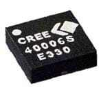
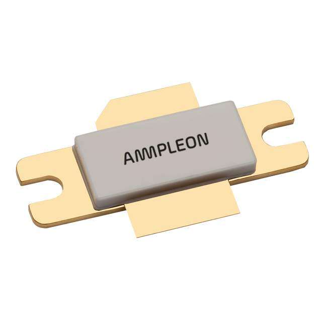
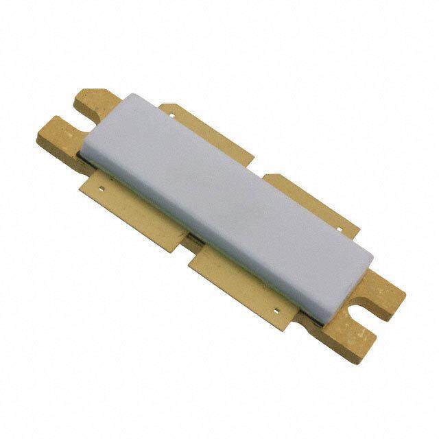
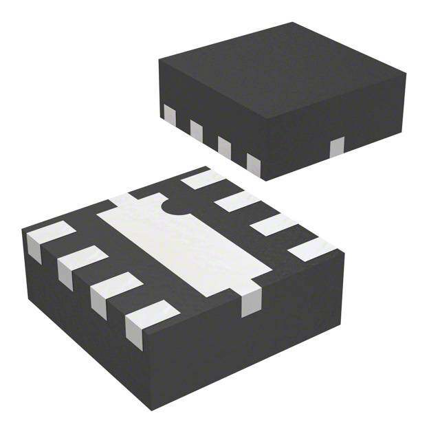
ICGOO电子元器件商城为您提供CGH40006S由Cree设计生产,在icgoo商城现货销售,并且可以通过原厂、代理商等渠道进行代购。 CGH40006S价格参考¥324.72-¥449.68。CreeCGH40006S封装/规格:晶体管 - FET,MOSFET - 射频, 射频 Mosfet HEMT 28V 100mA 0Hz ~ 6GHz 12dB 8W 6-QFN-EP(3x3)。您可以下载CGH40006S参考资料、Datasheet数据手册功能说明书,资料中有CGH40006S 详细功能的应用电路图电压和使用方法及教程。
Cree/Wolfspeed 的 CGH40006S 是一款基于氮化镓(GaN)高电子迁移率晶体管(HEMT)的射频功率MOSFET,广泛应用于高性能射频功率放大场景。其主要应用场景包括:

1. 无线通信基站:CGH40006S 在 2–6 GHz 频段表现出色,适用于4G LTE 和 5G 宏基站中的功率放大器模块,提供高效率和高线性度,满足现代移动通信对高数据速率和覆盖范围的需求。

2. 雷达系统:该器件具备高功率密度和优异的瞬时带宽性能,适合用于军用和民用雷达,如空中交通管制、气象雷达和相控阵雷达系统,提升探测距离与精度。

3. 工业与科学设备:在射频加热、等离子体生成和医疗设备(如射频消融)中,CGH40006S 可提供稳定可靠的高频大功率输出,提高系统能效与稳定性。

4. 宽带与多载波放大器:得益于其宽频带特性,该器件可用于宽带信号放大,支持多种通信标准的融合应用,如公共安全通信、专网通信等。

CGH40006S 采用 GaN on SiC 技术,具有高耐温性、高击穿电压和出色的热管理能力,可在高温和高负载环境下长期稳定运行,显著提升系统可靠性并降低冷却成本。因此,它成为现代高性能射频系统中替代传统LDMOS器件的理想选择。
| 参数 | 数值 |
| 产品目录 | |
| 描述 | FET RF HEMT 6GHZ 28V 3X3QFN |
| 产品分类 | RF FET |
| 品牌 | Cree Inc |
| 数据手册 | |
| 产品图片 |
|
| 产品型号 | CGH40006S |
| rohs | 无铅 / 符合限制有害物质指令(RoHS)规范要求 |
| 产品系列 | - |
| 供应商器件封装 | 6-QFN-EP(3x3) |
| 其它名称 | CGH40006SDKR |
| 功率-输出 | 8W |
| 包装 | Digi-Reel® |
| 噪声系数 | - |
| 增益 | 12dB |
| 封装/外壳 | 6-VDFN 裸露焊盘 |
| 晶体管类型 | HEMT |
| 标准包装 | 1 |
| 电压-测试 | 28V |
| 电压-额定 | 84V |
| 电流-测试 | 100mA |
| 频率 | 0Hz ~ 6GHz |
| 额定电流 | - |


- 商务部:美国ITC正式对集成电路等产品启动337调查
- 曝三星4nm工艺存在良率问题 高通将骁龙8 Gen1或转产台积电
- 太阳诱电将投资9.5亿元在常州建新厂生产MLCC 预计2023年完工
- 英特尔发布欧洲新工厂建设计划 深化IDM 2.0 战略
- 台积电先进制程称霸业界 有大客户加持明年业绩稳了
- 达到5530亿美元!SIA预计今年全球半导体销售额将创下新高
- 英特尔拟将自动驾驶子公司Mobileye上市 估值或超500亿美元
- 三星加码芯片和SET,合并消费电子和移动部门,撤换高东真等 CEO
- 三星电子宣布重大人事变动 还合并消费电子和移动部门
- 海关总署:前11个月进口集成电路产品价值2.52万亿元 增长14.8%


PDF Datasheet 数据手册内容提取
CGH40006S 6 W, RF Power GaN HEMT, Plastic Cree’s CGH40006S is an unmatched, gallium nitride (GaN) high electron mobility transistor (HEMT). The CGH40006S, operating from a 28 volt rail, offers a general purpose, broadband solution to a variety of RF and microwave applications. GaN HEMTs offer high efficiency, high gain and wide bandwidth capabilities making the CGH40006S ideal for linear and compressed amplifier circuits. The transistor is available in a 3mm x 3mm, surface mount, quad-flat-no-lead (QFN) package. Package Types: 440203 PN’s: CGH40006S FEATURES APPLICATIONS • Up to 6 GHz Operation • 2-Way Private Radio • 13 dB Small Signal Gain at 2.0 GHz • Broadband Amplifiers • 11 dB Small Signal Gain at 6.0 GHz • Cellular Infrastructure • 8 W typical at P = 32 dBm • Test Instrumentation IN • 65 % Efficiency at P = 32 dBm • Class A, AB, Linear amplifiers suitable for IN • 28 V Operation OFDM, W-CDMA, EDGE, CDMA waveforms • 3mm x 3mm Package 7 1 0 2 lir p A – 1 .3 v e R Subject to change without notice. 1 www.cree.com/wireless
Absolute Maximum Ratings (not simultaneous) at 25˚C Case Temperature Parameter Symbol Rating Units Conditions Drain-Source Voltage V 84 Volts 25˚C DSS Gate-to-Source Voltage V -10, +2 Volts 25˚C GS Storage Temperature T -65, +150 ˚C STG Operating Junction Temperature T 175 ˚C J Maximum Forward Gate Current I 2.1 mA 25˚C GMAX Maximum Drain Current1 I 0.75 A 25˚C DMAX Soldering Temperature2 T 260 ˚C S Thermal Resistance, Junction to Case3,4 R 10.1 ˚C/W 85˚C θJC Case Operating Temperature3,4 T -40, +150 ˚C C Note: 1 Current limit for long term, reliable operation 2 Refer to the Application Note on soldering at www.cree.com/RF/Document-Library 3 Measured for the CGH40006S at P = 8 W. DISS 4 T = Case temperature for the device. It refers to the temperature at the ground tab underneath the package. The PCB will add additional thermal C resistance. The RTH for Cree’s demonstration amplifier, CGH40006S-AMP1, with 13 (Ø20 mil) via holes designed on a 20 mil thick Rogers 5880 PCB, is 5.1°C. The total Rth from the heat sink to the junction is 10.1°C +5.1°C = 15.2 °C/W. Electrical Characteristics (T = 25˚C) C Characteristics Symbol Min. Typ. Max. Units Conditions DC Characteristics1 Gate Threshold Voltage V -3.8 -3.0 -2.3 V V = 10 V, I = 2.1 mA GS(th) DC DS D Gate Quiescent Voltage V – -2.7 – V V = 28 V, I = 100 mA GS(Q) DC DS D Saturated Drain Current I 1.7 2.1 – A V = 6.0 V, V = 2.0 V DS DS GS Drain-Source Breakdown Voltage V 120 – – V V = -8 V, I = 2.1 mA BR DC GS D RF Characteristics2 (T = 25˚C, F = 5.8 GHz unless otherwise noted) C 0 Small Signal Gain G 10 11.8 – dB V = 28 V, I = 100 mA SS DD DQ Power Output at P = 30 dBm P 5 6.9 – W V = 28 V, I = 100 mA IN OUT DD DQ Drain Efficiency3 η 40 53 – % V = 28 V, I = 100 mA, P = 30 dBm DD DQ IN No damage at all phase angles, Output Mismatch Stress VSWR – – 10 : 1 Y V = 28 V, I = 100 mA, DD DQ P = 32 dBm IN Dynamic Characteristics Input Capacitance C – 2.7 – pF V = 28 V, V = -8 V, f = 1 MHz GS DS gs Output Capacitance C – 0.8 – pF V = 28 V, V = -8 V, f = 1 MHz DS DS gs Feedback Capacitance C – 0.1 – pF V = 28 V, V = -8 V, f = 1 MHz GD DS gs Notes: 1 Measured on wafer prior to packaging. 2 Measured in Cree’s narrow band production test fixture AD-000291. This fixture is designed for high volume test at 5.8 GHz and may not show the full capability of the device due to source inductance and thermal performance. The demonstration amplifier, CGH40006S-AMP1, is a better indicator of the true RF performance of the device. 3 Drain Efficiency = P / P OUT DC Cree, Inc. 4600 Silicon Drive Copyright © 2010-2017 Cree, Inc. All rights reserved. The information in this document is subject to change without notice. Cree and the Cree logo are Durham, North Carolina, USA 27703 registered trademarks of Cree, Inc. USA Tel: +1.919.313.5300 Fax: +1.919.869.2733 2 CGH40006S Rev 3.1 www.cree.com/rf
Typical Performance Small Signal Gain vs Frequency at 28 V of the CGH40006S Sin-p tahrea mCGetHer40006S-AMP1 16 14 12 10 B)B) dd n(n( 8 aiai GG 6 4 CGH40006S-S21 2 0 1.0 1.5 2.0 2.5 3.0 3.5 4.0 4.5 5.0 5.5 6.0 Frequency(GHz) Input & Output Return Losses vs Frequency at 28 V of the CGH40006SS-p ianr athmee CteGrH40006S-AMP1 0 -2 -4 -6 -8 -10 B)B) dd--1122 (( nn aiai-14 GG -16 -18 -20 -22 CGH40006S-S11 -24 CGH40006S-S22 -26 1.0 1.5 2.0 2.5 3.0 3.5 4.0 4.5 5.0 5.5 6.0 Frequency(GHz) Cree, Inc. 4600 Silicon Drive Copyright © 2010-2017 Cree, Inc. All rights reserved. The information in this document is subject to change without notice. Cree and the Cree logo are Durham, North Carolina, USA 27703 registered trademarks of Cree, Inc. USA Tel: +1.919.313.5300 Fax: +1.919.869.2733 3 CGH40006S Rev 3.1 www.cree.com/rf
Typical Performance Power Gain vs Output Power as a Function of Frequency of the CGH40006S in the CGH40006S-AMP1 V = 28 V, I = 100 mA DD GainvDsQ.Pout 20 2.0GHz 18 3.0GHz 4.0GHz 16 5.0GHz 6.0GHz 14 12 B)B) dd n(n(10 aiai GG 8 6 4 2 0 20 22 24 26 28 30 32 34 36 38 40 OutputPower(dBm) Drain Efficiency vs Output Power as a Function of Frequency of the CGH40006S in the CGH40006S-AMP1 V = 28 V, I = 100 mA DDEFFvsouDtQputpower 70% 2.0GHz 60% 3.0GHz 4.0GHz 5.0GHz 50% 6.0GHz yy cc nn ee40% cici EffiEffi nn aiai30% DrDr 20% 10% 0% 20 22 24 26 28 30 32 34 36 38 40 OutputPower(dBm) Cree, Inc. 4600 Silicon Drive Copyright © 2010-2017 Cree, Inc. All rights reserved. The information in this document is subject to change without notice. Cree and the Cree logo are Durham, North Carolina, USA 27703 registered trademarks of Cree, Inc. USA Tel: +1.919.313.5300 Fax: +1.919.869.2733 4 CGH40006S Rev 3.1 www.cree.com/rf
Typical Performance Power Gain vs Input Power as a Function of Frequency of the CGH40006S in the CGH40006S-AMP1 V = 28 V, I = 100 mA DDGainvsinDQputpower 14 12 10 B)B) 8 dd (( nn aiai GG 6 2.0GHz 4 3.0GHz 4.0GHz 5.0GHz 2 6.0GHz 0 10 12 14 16 18 20 22 24 26 28 30 32 34 InputPower(dBm) Drain Efficiency vs Input Power as a Function of Frequency of the CGH40006S in the CGH40006S-AMP1 V D =ra 2in8E Vff,i cIien c=y 1v0s.0P minA DD DQ 100% 90% 2.0GHz 3.0GHz 80% 4.0GHz 5.0GHz 70% 6.0GHz yy cc 60% nn ee cici EffiEffi 50% nn aiai DrDr 40% 30% 20% 10% 0% 10 12 14 16 18 20 22 24 26 28 30 32 34 InputPower(dBm) Cree, Inc. 4600 Silicon Drive Copyright © 2010-2017 Cree, Inc. All rights reserved. The information in this document is subject to change without notice. Cree and the Cree logo are Durham, North Carolina, USA 27703 registered trademarks of Cree, Inc. USA Tel: +1.919.313.5300 Fax: +1.919.869.2733 5 CGH40006S Rev 3.1 www.cree.com/rf
Typical Performance Power Gain vs Frequency of the CGH40006S in the CGH40006S-AMP1 at P = 32 dBm, V = 28 V Gain@Pin32dINBm DD 10 9 8 7 6 B)B) dd n(n( 5 GaiGai 4 3 2 1 0 2.0 2.5 3.0 3.5 4.0 4.5 5.0 5.5 6.0 Frequency(GHz) Output Power vs Frequency of the CGH40006S in the CGH40006S-AMP1 at P = 32 dBm, V = 28 V IN DD Power(w)@Pin32dBm 12 10 8 W)W) wer(wer( PoPo 6 utut pp utut OO 4 2 0 2.0 2.5 3.0 3.5 4.0 4.5 5.0 5.5 6.0 Frequency(GHz) Drain Efficiency vs Frequency of the CGH40006S in the CGH40006S-AMP1 at P = 32 dBm, V = 28 V Drainefficiency@PiInN32dBm DD 70% 60% 50% EfficiencyEfficiency40% DrainDrain30% 20% 10% 0% 2.0 2.5 3.0 3.5 4.0 4.5 5.0 5.5 6.0 Frequency(GHz) Cree, Inc. 4600 Silicon Drive Copyright © 2010-2017 Cree, Inc. All rights reserved. The information in this document is subject to change without notice. Cree and the Cree logo are Durham, North Carolina, USA 27703 registered trademarks of Cree, Inc. USA Tel: +1.919.313.5300 Fax: +1.919.869.2733 6 CGH40006S Rev 3.1 www.cree.com/rf
Typical Performance Third Order Intermodulation Distortion vs Average Output Power as a Function of Frequency of the CGH40006S in the CGH40006S-AMP1 IVM3 =vs 2T8o Vta, lIou =tp 6u0t pmoAwer DD DQ 0 2.0GHz -10 3.0GHz 4.0GHz 5.0GHz -20 6.0GHz c)c) BB (d(d-30 33 MM II -40 -50 -60 20 21 22 23 24 25 26 27 28 29 30 31 32 33 34 35 36 37 OutputPower(dBm) Electrostatic Discharge (ESD) Classifications Parameter Symbol Class Test Methodology Human Body Model HBM 1A (> 250 V) JEDEC JESD22 A114-D Charge Device Model CDM 2 (125 V to 250 V) JEDEC JESD22 C101-C Moisture Sensitivity Level (MSL) Classification Parameter Symbol Level Test Methodology Moisture Sensitivity Level MSL 3 (168 hours) IPC/JEDEC J-STD-20 Cree, Inc. 4600 Silicon Drive Copyright © 2010-2017 Cree, Inc. All rights reserved. The information in this document is subject to change without notice. Cree and the Cree logo are Durham, North Carolina, USA 27703 registered trademarks of Cree, Inc. USA Tel: +1.919.313.5300 Fax: +1.919.869.2733 7 CGH40006S Rev 3.1 www.cree.com/rf
Typical Performance Simulated Maximum Available Gain and K Factor of the CGH40006S V = 28 V, I = 100 mA DD DQ ) r B o d ct G ( Fa A K M Note 1. On a 20 mil thick PCB. Typical Noise Performance Simulated Minimum Noise Figure and Noise Resistance vs Frequency of the CGH40006S V = 28 V, I = 100 mA DD DQ ) B ) d s ( m e h ur O g ( i e F c e n s a oi st N si m e R u m e s ni oi Mi N Note 1. On a 20 mil thick PCB. Cree, Inc. 4600 Silicon Drive Copyright © 2010-2017 Cree, Inc. All rights reserved. The information in this document is subject to change without notice. Cree and the Cree logo are Durham, North Carolina, USA 27703 registered trademarks of Cree, Inc. USA Tel: +1.919.313.5300 Fax: +1.919.869.2733 8 CGH40006S Rev 3.1 www.cree.com/rf
CGH40006S CW Power Dissipation De-rating Curve PowerDissipationderatingCurvevsmaxTcase 10 9 8 7 W) ( on 6 ati p si 5 s Di er 4 w o P 3 Note 1 2 1 0 0 25 50 75 100 125 150 175 200 MaximumCaseTemperature(°C) Note 1. Area exceeds Maximum Case Operating Temperature (See Page 2). Source and Load Impedances D Z Source Z Load G S Frequency (MHz) Z Source Z Load 1000 12.7 + j20.2 62.3 + j42 2000 5.98 + j6.81 32.7 + j32.9 3000 3.32 - j2.89 19.2 + j29.8 4000 2.38 - j9.45 15.2 + j15.7 5000 2.62 - j15.6 9.98 + j9.6 6000 1.94 - j21.35 8.51 + j2.07 Note 1. V = 28V, I = 100mA in the 440203 package. DD DQ Note 2. Optimized for power gain, P and PAE. SAT Note 3. When using this device at low frequency, series resistors should be used to maintain amplifier stability. Note 4. 35 pH source inductance is assumed between the package and RF ground (20 mil thick PCB). Cree, Inc. 4600 Silicon Drive Copyright © 2010-2017 Cree, Inc. All rights reserved. The information in this document is subject to change without notice. Cree and the Cree logo are Durham, North Carolina, USA 27703 registered trademarks of Cree, Inc. USA Tel: +1.919.313.5300 Fax: +1.919.869.2733 9 CGH40006S Rev 3.1 www.cree.com/rf
CGH40006S-AMP1 Demonstration Amplifier Circuit Bill of Materials Designator Description Qty R1 RES, AIN, 0505, 470 Ohms (≤5% tolerance) 1 R2 RES, AIN, 0505, 50 Ohms (≤5% tolerance) 1 R3 RES, AIN, 0505, 360 Ohms (≤5% tolerance) 1 C1 CAP, 1.3 pF +/-0.1 pF, 0603, ATC 600S 1 C2 CAP, 2.7 pF +/-0.25 pF, 0603, ATC 600S 1 C10 CAP, 3.6 pF +/-0.1 pF, 0603, ATC 600S 1 C4,C11 CAP, 8.2 pF +/-0.25, 0603, ATC 600S 2 C6,C13 CAP, 470 pF +/-5%, 0603, 100 V 2 C7,C14 CAP, 33000 pF, CER, 100V, X7R, 0805 2 C8 CAP, 10 uf, 16V, SMT, TANTALUM 1 C15 CAP, 1.0 uF +/-10%, CER, 100V, X7R, 1210 1 C16 CAP, 33 uF, 100V, ELECT, FK, SMD 1 J3,J4 CONN, SMA, STR, PANEL, JACK, RECP 2 J1 HEADER RT>PLZ .1CEN LK 5POS 1 - PCB, RO5880, 0.020” THK 1 Q1 CGH40006S 1 CGH40006S-AMP1 Demonstration Amplifier Circuit Cree, Inc. 4600 Silicon Drive Copyright © 2010-2017 Cree, Inc. All rights reserved. The information in this document is subject to change without notice. Cree and the Cree logo are Durham, North Carolina, USA 27703 registered trademarks of Cree, Inc. USA Tel: +1.919.313.5300 Fax: +1.919.869.2733 10 CGH40006S Rev 3.1 www.cree.com/rf
CGH40006S-AMP1 Demonstration Amplifier Circuit Schematic CGH40006S-AMP1 Demonstration Amplifier Circuit Outline Cree, Inc. 4600 Silicon Drive Copyright © 2010-2017 Cree, Inc. All rights reserved. The information in this document is subject to change without notice. Cree and the Cree logo are Durham, North Carolina, USA 27703 registered trademarks of Cree, Inc. USA Tel: +1.919.313.5300 Fax: +1.919.869.2733 11 CGH40006S Rev 3.1 www.cree.com/rf
Typical Package S-Parameters for CGH40006S (Small Signal, V = 28 V, I = 100 mA, angle in degrees) DS DQ Frequency Mag S11 Ang S11 Mag S21 Ang S21 Mag S12 Ang S12 Mag S22 Ang S22 500 MHz 0.933 -92.95 18.74 125.47 0.024 38.02 0.459 -48.87 600 MHz 0.922 -104.26 16.89 118.64 0.026 31.70 0.428 -54.78 700 MHz 0.912 -113.77 15.28 112.75 0.028 26.33 0.402 -59.82 800 MHz 0.905 -121.83 13.90 107.61 0.029 21.71 0.381 -64.21 900 MHz 0.899 -128.73 12.70 103.06 0.030 17.68 0.365 -68.10 1.0 GHz 0.894 -134.72 11.67 98.96 0.030 14.11 0.352 -71.62 1.1 GHz 0.891 -139.97 10.77 95.23 0.030 10.91 0.342 -74.86 1.2 GHz 0.888 -144.62 9.99 91.80 0.031 8.00 0.334 -77.87 1.3 GHz 0.886 -148.78 9.31 88.61 0.031 5.34 0.328 -80.72 1.4 GHz 0.884 -152.55 8.71 85.61 0.031 2.88 0.325 -83.43 1.5 GHz 0.883 -155.97 8.17 82.77 0.031 0.58 0.322 -86.03 1.6 GHz 0.881 -159.12 7.69 80.07 0.031 -1.57 0.321 -88.54 1.7 GHz 0.881 -162.04 7.26 77.49 0.031 -3.60 0.321 -90.98 1.8 GHz 0.880 -164.75 6.88 75.00 0.031 -5.53 0.321 -93.35 1.9 GHz 0.879 -167.29 6.53 72.60 0.031 -7.38 0.323 -95.67 2.0 GHz 0.879 -169.68 6.21 70.26 0.031 -9.14 0.325 -97.94 2.1 GHz 0.879 -171.94 5.92 68.00 0.030 -10.83 0.327 -100.17 2.2 GHz 0.879 -174.09 5.65 65.79 0.030 -12.46 0.330 -102.36 2.3 GHz 0.879 -176.14 5.40 63.62 0.030 -14.03 0.334 -104.51 2.4 GHz 0.879 -178.10 5.18 61.51 0.030 -15.55 0.338 -106.63 2.5 GHz 0.879 -179.98 4.97 59.43 0.030 -17.02 0.342 -108.71 2.6 GHz 0.879 178.20 4.77 57.38 0.029 -18.44 0.346 -110.77 2.7 GHz 0.879 176.44 4.59 55.37 0.029 -19.83 0.351 -112.81 2.8 GHz 0.879 174.74 4.42 53.39 0.029 -21.18 0.355 -114.82 2.9 GHz 0.879 173.09 4.26 51.43 0.029 -22.48 0.360 -116.80 3.0 GHz 0.880 171.49 4.11 49.50 0.028 -23.76 0.366 -118.76 3.2 GHz 0.880 168.39 3.84 45.70 0.028 -26.20 0.376 -122.63 3.4 GHz 0.881 165.43 3.60 41.97 0.027 -28.51 0.387 -126.41 3.6 GHz 0.882 162.57 3.38 38.31 0.026 -30.70 0.399 -130.13 3.8 GHz 0.883 159.81 3.19 34.71 0.025 -32.75 0.410 -133.78 4.0 GHz 0.884 157.13 3.01 31.16 0.025 -34.68 0.422 -137.38 4.2 GHz 0.885 154.52 2.85 27.65 0.024 -36.47 0.433 -140.91 4.4 GHz 0.887 151.96 2.71 24.19 0.023 -38.12 0.445 -144.40 4.6 GHz 0.888 149.45 2.57 20.77 0.022 -39.63 0.457 -147.84 4.8 GHz 0.889 146.98 2.45 17.38 0.022 -40.97 0.468 -151.24 5.0 GHz 0.890 144.55 2.33 14.03 0.021 -42.15 0.480 -154.60 5.2 GHz 0.892 142.15 2.23 10.71 0.020 -43.15 0.491 -157.92 5.4 GHz 0.893 139.78 2.13 7.41 0.019 -43.95 0.503 -161.20 5.6 GHz 0.894 137.43 2.04 4.15 0.018 -44.53 0.514 -164.45 5.8 GHz 0.896 135.11 1.95 0.91 0.018 -44.89 0.525 -167.66 6.0 GHz 0.897 132.80 1.87 -2.30 0.017 -45.00 0.535 -170.85 To download the s-parameters in s2p format, go to the CGH40006S Product Page and click on the documentation tab. Note 2. On a 20 mil thick PCB. Cree, Inc. 4600 Silicon Drive Copyright © 2010-2017 Cree, Inc. All rights reserved. The information in this document is subject to change without notice. Cree and the Cree logo are Durham, North Carolina, USA 27703 registered trademarks of Cree, Inc. USA Tel: +1.919.313.5300 Fax: +1.919.869.2733 12 CGH40006S Rev 3.1 www.cree.com/rf
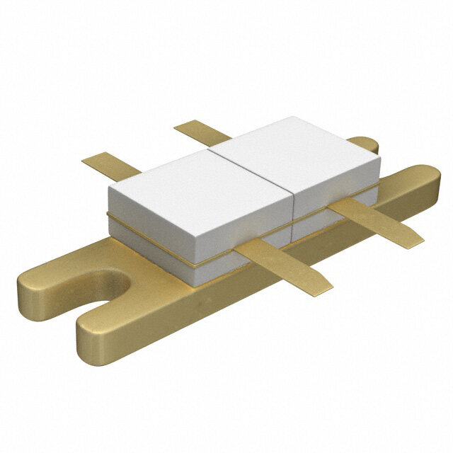
Product Dimensions CGH40006S (Package Type — 440203) Pin Input/Output 1 GND 2 RF IN 3 GND 4 GND 5 RF OUT 6 GND Cree, Inc. 4600 Silicon Drive Copyright © 2010-2017 Cree, Inc. All rights reserved. The information in this document is subject to change without notice. Cree and the Cree logo are Durham, North Carolina, USA 27703 registered trademarks of Cree, Inc. USA Tel: +1.919.313.5300 Fax: +1.919.869.2733 13 CGH40006S Rev 3.1 www.cree.com/rf
Tape & Reel Dimensions Cree, Inc. 4600 Silicon Drive Copyright © 2010-2017 Cree, Inc. All rights reserved. The information in this document is subject to change without notice. Cree and the Cree logo are Durham, North Carolina, USA 27703 registered trademarks of Cree, Inc. USA Tel: +1.919.313.5300 Fax: +1.919.869.2733 14 CGH40006S Rev 3.1 www.cree.com/rf
Product Ordering Information Order Number Description Unit of Measure CGH40006S GaN HEMT Each CGH40006S-AMP1 Test board with GaN HEMT installed Each CGH40006S-TR Delivered in Tape and Reel 200 parts / reel Cree, Inc. 4600 Silicon Drive Copyright © 2010-2017 Cree, Inc. All rights reserved. The information in this document is subject to change without notice. Cree and the Cree logo are Durham, North Carolina, USA 27703 registered trademarks of Cree, Inc. USA Tel: +1.919.313.5300 Fax: +1.919.869.2733 15 CGH40006S Rev 3.1 www.cree.com/rf
Disclaimer Specifications are subject to change without notice. Cree, Inc. believes the information contained within this data sheet to be accurate and reliable. However, no responsibility is assumed by Cree for any infringement of patents or other rights of third parties which may result from its use. No license is granted by implication or otherwise under any patent or patent rights of Cree. Cree makes no warranty, representation or guarantee regarding the suitability of its products for any particular purpose. “Typical” parameters are the average values expected by Cree in large quantities and are provided for information purposes only. These values can and do vary in different applications and actual performance can vary over time. All operating parameters should be validated by customer’s technical experts for each application. Cree products are not designed, intended or authorized for use as components in applications intended for surgical implant into the body or to support or sustain life, in applications in which the failure of the Cree product could result in personal injury or death or in applications for planning, construction, maintenance or direct operation of a nuclear facility. For more information, please contact: Cree, Inc. 4600 Silicon Drive Durham, North Carolina, USA 27703 www.cree.com/RF Sarah Miller Marketing & Export Cree, RF Components 1.919.407.5302 Ryan Baker Marketing Cree, Wireless Devices 1.919.407.7816 Tom Dekker Sales Director Cree, Wireless Devices 1.919.407.5639 Cree, Inc. 4600 Silicon Drive Copyright © 2010-2017 Cree, Inc. All rights reserved. The information in this document is subject to change without notice. Cree and the Cree logo are Durham, North Carolina, USA 27703 registered trademarks of Cree, Inc. USA Tel: +1.919.313.5300 Fax: +1.919.869.2733 16 CGH40006S Rev 3.1 www.cree.com/rf
Mouser Electronics Authorized Distributor Click to View Pricing, Inventory, Delivery & Lifecycle Information: C ree, Inc.: CGH40006S-KIT CGH40006S