ICGOO在线商城 > 分立半导体产品 > 晶体管 - FET,MOSFET - 射频 > MRF1518NT1
 Datasheet下载
- 型号: MRF1518NT1
- 制造商: Freescale Semiconductor
- 库位|库存: xxxx|xxxx
- 要求:
| 数量阶梯 | 香港交货 | 国内含税 |
| +xxxx | $xxxx | ¥xxxx |
查看当月历史价格
查看今年历史价格
MRF1518NT1产品简介:
ICGOO电子元器件商城为您提供MRF1518NT1由Freescale Semiconductor设计生产,在icgoo商城现货销售,并且可以通过原厂、代理商等渠道进行代购。 MRF1518NT1价格参考¥32.94-¥51.61。Freescale SemiconductorMRF1518NT1封装/规格:晶体管 - FET,MOSFET - 射频, RF Mosfet LDMOS 12.5V 150mA 520MHz 13dB 8W PLD-1.5。您可以下载MRF1518NT1参考资料、Datasheet数据手册功能说明书,资料中有MRF1518NT1 详细功能的应用电路图电压和使用方法及教程。
MRF1518NT1是NXP USA Inc.生产的一款射频MOSFET晶体管,属于高功率LDMOS(横向扩散金属氧化物半导体)器件,主要应用于高频、高功率的射频放大场合。该器件典型工作频率范围覆盖1.8 GHz至2.2 GHz,适合用于蜂窝通信基础设施中的基站功率放大器。

其主要应用场景包括4G LTE和5G移动通信网络的宏基站和微波中继系统,作为输出级的主放大器,提供高效率和高线性度的信号放大能力。此外,MRF1518NT1也广泛用于工业、科学和医疗(ISM)频段设备,如射频能量应用、等离子发生器和加热系统等需要稳定射频功率输出的场合。

该器件采用先进的封装技术,具备良好的热稳定性和可靠性,可在高电压和大电流条件下长期运行,适用于严苛的工业环境。其高增益和优异的互调失真性能,有助于提升通信系统的信号质量和覆盖范围。

总之,MRF1518NT1是一款面向现代无线通信和射频能源应用的高性能器件,特别适用于要求高输出功率、高效率和高可靠性的射频功率放大设计。
| 参数 | 数值 |
| 产品目录 | |
| 描述 | MOSFET RF N-CH PLD-1.5射频MOSFET晶体管 RF LDMOS FET PLD1.5N |
| 产品分类 | RF FET分离式半导体 |
| Id-ContinuousDrainCurrent | 4 A |
| Id-连续漏极电流 | 4 A |
| 品牌 | Freescale Semiconductor |
| 产品手册 | |
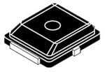
| 产品图片 |
|
| rohs | 符合RoHS库存产品核实请求 / 库存产品核实请求 |
| 产品系列 | 晶体管,晶体管射频,射频MOSFET晶体管,Freescale Semiconductor MRF1518NT1- |
| 数据手册 | |
| 产品型号 | MRF1518NT1 |
| PCN封装 | http://cache.freescale.com/files/shared/doc/pcn/PCN15687.htm |
| Pd-PowerDissipation | 62.5 W |
| Pd-功率耗散 | 62.5 W |
| Vds-Drain-SourceBreakdownVoltage | 40 V |
| Vds-漏源极击穿电压 | 40 V |
| Vgs-Gate-SourceBreakdownVoltage | +/- 20 V |
| Vgs-栅源极击穿电压 | +/- 20 V |
| Vgsth-Gate-SourceThresholdVoltage | 1.6 V |
| Vgsth-栅源极阈值电压 | 1.6 V |
| 产品目录页面 | |
| 产品种类 | 射频MOSFET晶体管 |
| 产品类型 | RF MOSFET Power |
| 供应商器件封装 | PLD-1.5 |
| 其它名称 | MRF1518NT1DKR |
| 功率-输出 | 8W |
| 功率耗散 | 62.5 W |
| 包装 | Digi-Reel® |
| 单位重量 | 280 mg |
| 商标 | Freescale Semiconductor |
| 噪声系数 | - |
| 增益 | 13dB |
| 安装风格 | SMD/SMT |
| 封装 | Reel |
| 封装/外壳 | PLD-1.5 |
| 封装/箱体 | PLD-1.5 |
| 工厂包装数量 | 1000 |
| 技术 | MOSFET |
| 晶体管极性 | N-Channel |
| 晶体管类型 | LDMOS |
| 最大工作温度 | + 150 C |
| 最小工作温度 | - 65 C |
| 标准包装 | 1 |
| 汲极/源极击穿电压 | 40 V |
| 漏极连续电流 | 4 A |
| 电压-测试 | 12.5V |
| 电压-额定 | 40V |
| 电流-测试 | 150mA |
| 系列 | MRF1518NT1 |
| 输出功率 | 8 W |
| 配置 | Single |
| 闸/源击穿电压 | +/- 20 V |
| 频率 | 520MHz |
| 额定电流 | 4A |


- 商务部:美国ITC正式对集成电路等产品启动337调查
- 曝三星4nm工艺存在良率问题 高通将骁龙8 Gen1或转产台积电
- 太阳诱电将投资9.5亿元在常州建新厂生产MLCC 预计2023年完工
- 英特尔发布欧洲新工厂建设计划 深化IDM 2.0 战略
- 台积电先进制程称霸业界 有大客户加持明年业绩稳了
- 达到5530亿美元!SIA预计今年全球半导体销售额将创下新高
- 英特尔拟将自动驾驶子公司Mobileye上市 估值或超500亿美元
- 三星加码芯片和SET,合并消费电子和移动部门,撤换高东真等 CEO
- 三星电子宣布重大人事变动 还合并消费电子和移动部门
- 海关总署:前11个月进口集成电路产品价值2.52万亿元 增长14.8%


PDF Datasheet 数据手册内容提取
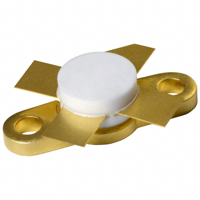
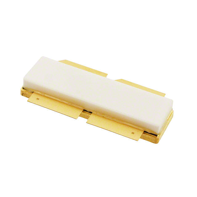
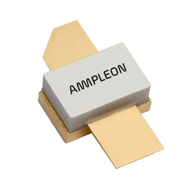
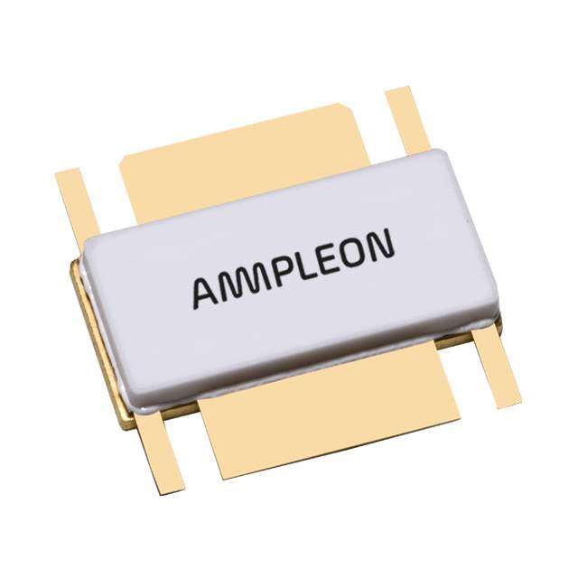
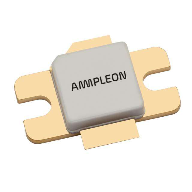
Freescale Semiconductor Document Number: MRF1518N Technical Data Rev. 11, 6/2009 RF Power Field Effect Transistor N-Channel Enhancement-Mode Lateral MOSFET MRF1518NT1 Designed for broadband commercial and industrial applications with frequen- cies to 520 MHz. The high gain and broadband performance of this device make it ideal for large-signal, common source amplifier applications in 12.5 volt mobile FM equipment. • Specified Performance @ 520 MHz, 12.5 Volts D Output Power (cid:151) 8 Watts Power Gain (cid:151) 13 dB 520 MHz, 8 W, 12.5 V Efficiency (cid:151) 60% LATERAL N-CHANNEL • Capable of Handling 20:1 VSWR, @ 15.5 Vdc, BROADBAND 520 MHz, 2 dB Overdrive RF POWER MOSFET Features • Excellent Thermal Stability G • Characterized with Series Equivalent Large-Signal Impedance Parameters • N Suffix Indicates Lead-Free Terminations. RoHS Compliant. • In Tape and Reel. T1 Suffix = 1,000 Units per 12 mm, S 7 inch Reel. CASE 466-03, STYLE 1 PLD-1.5 PLASTIC Table 1. Maximum Ratings Rating Symbol Value Unit Drain-Source Voltage VDSS -0.5, +40 Vdc Gate-Source Voltage VGS ±20 Vdc Drain Current (cid:151) Continuous ID 4 Adc Total Device Dissipation @ TC = 25°C (1) PD 62.5 W Derate above 25°C 0.50 W/°C Storage Temperature Range Tstg -65 to +150 °C Operating Junction Temperature TJ 150 °C Table 2. Thermal Characteristics Characteristic Symbol Value (2) Unit Thermal Resistance, Junction to Case RθJC 2 °C/W Table 3. Moisture Sensitivity Level Test Methodology Rating Package Peak Temperature Unit Per JESD22-A113, IPC/JEDEC J-STD-020 3 260 °C TJ(cid:150)TC 1. Calculated based on the formula PD = RθJC 2. MTTF calculator available at http://www.freescale.com/rf. Select Software & Tools/Development Tools/Calculators to access MTTF calculators by product. NOTE - CAUTION - MOS devices are susceptible to damage from electrostatic charge. Reasonable precautions in handling and packaging MOS devices should be observed. © Freescale Semiconductor, Inc., 2008-2009. All rights reserved. MRF1518NT1 RF Device Data Freescale Semiconductor 1
Table 4. Electrical Characteristics (TA = 25°C unless otherwise noted) Characteristic Symbol Min Typ Max Unit Off Characteristics Zero Gate Voltage Drain Current IDSS (cid:151) (cid:151) 1 μAdc (VDS = 40 Vdc, VGS = 0 Vdc) Gate-Source Leakage Current IGSS (cid:151) (cid:151) 1 μAdc (VGS = 10 Vdc, VDS = 0 Vdc) On Characteristics Gate Threshold Voltage VGS(th) 1 1.6 2.1 Vdc (VDS = 12.5 Vdc, ID = 100 μA) Drain-Source On-Voltage VDS(on) (cid:151) 0.4 (cid:151) Vdc (VGS = 10 Vdc, ID = 1 Adc) Dynamic Characteristics Input Capacitance Ciss (cid:151) 66 (cid:151) pF (VDS = 12.5 Vdc, VGS = 0, f = 1 MHz) Output Capacitance Coss (cid:151) 33 (cid:151) pF (VDS = 12.5 Vdc, VGS = 0, f = 1 MHz) Reverse Transfer Capacitance Crss (cid:151) 4.5 (cid:151) pF (VDS = 12.5 Vdc, VGS = 0, f = 1 MHz) Functional Tests (In Freescale Test Fixture) Common-Source Amplifier Power Gain Gps (cid:151) 13 (cid:151) dB (VDD = 12.5 Vdc, Pout = 8 Watts, IDQ = 150 mA, f = 520 MHz) Drain Efficiency η (cid:151) 60 (cid:151) % (VDD = 12.5 Vdc, Pout = 8 Watts, IDQ = 150 mA, f = 520 MHz) MRF1518NT1 RF Device Data 2 Freescale Semiconductor
B2 VGG C8 C7 +C6 R4 B1 + VDD R3 C16 C15 C14 C13 L1 C5 R2 N2 Z6 Z7 Z8 Z9 Z10 RF R1 N1 DUT C12 OUTPUT RF Z1 Z2 Z3 Z4 Z5 INPUT C9 C10 C11 C1 C2 C3 C4 B1, B2 Short Ferrite Beads, Fair Rite Products R4 33 kΩ, 1/8 W Resistor (2743021446) Z1 0.451″ x 0.080″ Microstrip C1, C12 240 pF, 100 mil Chip Capacitors Z2 1.005″ x 0.080″ Microstrip C2, C3, C10, C11 0 to 20 pF Trimmer Capacitors Z3 0.020″ x 0.080″ Microstrip C4 82 pF, 100 mil Chip Capacitor Z4 0.155″ x 0.080″ Microstrip C5, C16 120 pF, 100 mil Chip Capacitors Z5, Z6 0.260″ x 0.223″ Microstrip C6, C13 10 μF, 50 V Electrolytic Capacitors Z7 0.065″ x 0.080″ Microstrip C7, C14 1,200 pF, 100 mil Chip Capacitors Z8 0.266″ x 0.080″ Microstrip C8, C15 0.1 (cid:2)F, 100 mil Chip Capacitors Z9 1.113″ x 0.080″ Microstrip C9 30 pF, 100 mil Chip Capacitor Z10 0.433″ x 0.080″ Microstrip ® L1 55.5 nH, 5 Turn, Coilcraft Board Glass Teflon , 31 mils, 2 oz. Copper N1, N2 Type N Flange Mounts R1 15 Ω Chip Resistor (0805) R2 51 Ω, 1/2 W Resistor R3 10 Ω Chip Resistor (0805) Figure 1. 450 - 520 MHz Broadband Test Circuit TYPICAL CHARACTERISTICS, 450 - 520 MHz 12 0 VDD = 12.5 Vdc R (WATTS) 180 470 MHz 450 MHz LOSS (dB) −5 WE 500 MHz RN 470 MHz PO 6 TU −10 PUT 520 MHz T RE 450 MHz 500 MHz UT 4 PU O N , ut L, I −15 Po 2 IR 520 MHz VDD = 12.5 Vdc 0 −20 0 0.1 0.2 0.3 0.4 0.5 0.6 0 1 2 3 4 5 6 7 8 9 10 11 Pin, INPUT POWER (WATTS) Pout, OUTPUT POWER (WATTS) Figure 2. Output Power versus Input Power Figure 3. Input Return Loss versus Output Power MRF1518NT1 RF Device Data Freescale Semiconductor 3
TYPICAL CHARACTERISTICS, 450 - 520 MHz 17 80 450 MHz 470 MHz 470 MHz 70 450 MHz 15 %) 60 13 520 MHz CY ( N 50 N (dB) 11 500 MHz FFICIE 40 520 MHz GAI N E 500 MHz AI 30 9 R D 7 Eff, 20 VDD = 12.5 Vdc 10 VDD = 12.5 Vdc 5 0 0 1 2 3 4 5 6 7 8 9 10 11 0 1 2 3 4 5 6 7 8 9 10 11 12 Pout, OUTPUT POWER (WATTS) Pout, OUTPUT POWER (WATTS) Figure 4. Gain versus Output Power Figure 5. Drain Efficiency versus Output Power 12 70 470 MHz 65 S) 10 470 MHz WATT 450 MHz Y (%) 60 450 MHz 500 MHz R ( 8 NC WE 520 MHz CIE 55 520 MHz PO 6 500 MHz FFI 50 T E U N TP AI 45 OU 4 DR , ut Eff, 40 Po 2 VPDinD = = 2 162.2.5 d VBdmc 35 VPDinD = = 2 162.2.5 d VBdmc 0 30 0 200 400 600 800 1000 0 200 400 600 800 1000 IDQ, BIASING CURRENT (mA) IDQ, BIASING CURRENT (mA) Figure 6. Output Power versus Biasing Current Figure 7. Drain Efficiency versus Biasing Current 12 80 470 MHz 11 450 MHz 75 S) TT 10 %) 70 470 MHz R (WA 9 NCY ( 65 WE 8 CIE 60 450 MHz T PO 7 EFFI 55 520 MHz U N TP 6 AI 50 500 MHz U 520 MHz R , Out 5 500 MHz Eff, D 45 Po 4 IDQ = 150 mA 40 IDQ = 150 mA 3 Pin = 26.2 dBm 35 Pin = 26.2 dBm 2 30 8 9 10 11 12 13 14 15 16 8 9 10 11 12 13 14 15 16 VDD, SUPPLY VOLTAGE (VOLTS) VDD, SUPPLY VOLTAGE (VOLTS) Figure 8. Output Power versus Supply Voltage Figure 9. Drain Efficiency versus Supply Voltage MRF1518NT1 RF Device Data 4 Freescale Semiconductor
B1 B2 VGG VDD + + C8 C7 C6 C5 C12 C13 C14 C15 L1 R1 N1 DUT N2 RF Z1 Z2 Z3 Z4 Z5 Z6 Z7 Z8 RF INPUT OUTPUT C1 C11 L2 C2 C3 C4 C9 C10 B1, B2 Long Ferrite Beads, Fair Rite Products N1, N2 Type N Flange Mounts C1, C9 12 pF, 100 mil Chip Capacitors R1 47 Ω Chip Resistor (0805) C2 6.8 pF, 100 mil Chip Capacitor Z1 1.145″ x 0.080″ Microstrip C3, C4 20 pF, 100 mil Chip Capacitors Z2 0.786″ x 0.080″ Microstrip C5 51 pF, 100 mil Chip Capacitor Z3 0.115″ x 0.223″ Microstrip C6, C13 1000 pF, 100 mil Chip Capacitors Z4 0.145″ x 0.223″ Microstrip C7, C14 0.039 μF, 100 mil Chip Capacitors Z5 0.260″ x 0.223″ Microstrip C8 1 μF, 20 V Tantalum Chip Capacitor Z6 0.081″ x 0.080″ Microstrip C10 3 pF, 100 mil Chip Capacitor Z7 0.104″ x 0.080″ Microstrip C11, C12 51 pF, 100 mil Chip Capacitors Z8 1.759″ x 0.080″ Microstrip C15 22 μF, 35 V Tantalum Chip Capacitor Board Glass Teflon®, 31 mils, 2 oz. Copper L1, L2 18.5 nH, 5 Turn, Coilcraft Figure 10. 820 - 850 MHz Broadband Test Circuit TYPICAL CHARACTERISTICS, 820 - 850 MHz 12 0 VDD = 12.5 Vdc R (WATTS) 108 830 MH8z40 MHz 850 MHz LOSS (dB) −10 850 MHz WE RN 840 MHz PO 6 820 MHz TU −20 T E U R UTP 4 PUT 820 MHz O N , ut L, I −30 Po 2 IR VDD = 12.5 Vdc 830 MHz 0 −40 0 0.1 0.2 0.3 0.4 0.5 0.6 1 2 3 4 5 6 7 8 9 10 11 12 Pin, INPUT POWER (WATTS) Pout, OUTPUT POWER (WATTS) Figure 11. Output Power versus Input Power Figure 12. Input Return Loss versus Output Power MRF1518NT1 RF Device Data Freescale Semiconductor 5
TYPICAL CHARACTERISTICS, 820 - 850 MHz 17 80 850 MHz 850 MHz 840 MHz 70 15 840 MHz %) 60 Y ( 13 C N 50 820 MHz N (dB) 11 830 MHz 820 MHz FFICIE 40 GAI N E 830 MHz AI 30 9 R D Eff, 20 7 10 VDD = 12.5 Vdc VDD = 12.5 Vdc 5 0 1 2 3 4 5 6 7 8 9 10 11 12 1 2 3 4 5 6 7 8 9 10 11 12 Pout, OUTPUT POWER (WATTS) Pout, OUTPUT POWER (WATTS) Figure 13. Gain versus Output Power Figure 14. Drain Efficiency versus Output Power 12 70 850 MHz 830 MHz S) 10 840 MHz 60 TT %) ER (WA 8 850 MHz ENCY ( 50 840 MHz 830 MHz 820 MHz POW 6 820 MHz FFICI 40 T E U N 30 TP AI U 4 R O D , ut Eff, 20 Po 2 10 VDD = 12.5 Vdc VDD = 12.5 Vdc 0 0 0 200 400 600 800 1000 0 200 400 600 800 1000 IDQ, BIASING CURRENT (mA) IDQ, BIASING CURRENT (mA) Figure 15. Output Power versus Figure 16. Drain Efficiency versus Biasing Current Biasing Current 12 80 11 75 S) 840 MHz 840 MHz TT 10 %) 70 R (WA 9 830 MHz NCY ( 65 850 MHz WE 8 CIE 60 T PO 7 820 MHz EFFI 55 830 MHz U N TP 6 AI 50 U 850 MHz R , Out 5 Eff, D 45 820 MHz Po 4 40 3 VDD = 12.5 Vdc 35 VDD = 12.5 Vdc 2 30 8 9 10 11 12 13 14 15 16 8 9 10 11 12 13 14 15 16 VDD, SUPPLY VOLTAGE (VOLTS) VDD, SUPPLY VOLTAGE (VOLTS) Figure 17. Output Power versus Figure 18. Drain Efficiency versus Supply Voltage Supply Voltage MRF1518NT1 RF Device Data 6 Freescale Semiconductor
B2 VGG C10 C9 +C8 R4 B1 + VDD C18 C17 C16 C15 R3 L1 C7 R2 N2 Z7 Z8 Z9 Z10 Z11 RF R1 RF N1 Z1 Z2 Z3 Z4 Z5 Z6 DUT C14 OUTPUT INPUT C11 C12 C13 C1 C2 C3 C4 C5 C6 B1, B2 Short Ferrite Beads, Fair Rite Products R3 10 Ω Chip Resistor (0805) (2743021446) R4 33 kΩ, 1/8 W Resistor C1, C14 240 pF, 100 mil Chip Capacitors Z1 0.476″ x 0.080″ Microstrip C2, C3, C4, C11, Z2 0.724″ x 0.080″ Microstrip C12, C13 0 to 20 pF Trimmer Capacitors Z3 0.348″ x 0.080″ Microstrip C5 30 pF, 100 mil Chip Capacitor Z4 0.048″ x 0.080″ Microstrip C6 47 pF, 100 mil Chip Capacitor Z5 0.175″ x 0.080″ Microstrip C7, C18 120 pF, 100 mil Chip Capacitors Z6, Z7 0.260″ x 0.223″ Microstrip C8, C15 10 μF, 50 V Electrolytic Capacitors Z8 0.239″ x 0.080″ Microstrip C9, C16 1,200 pF, 100 mil Chip Capacitors Z9 0.286″ x 0.080″ Microstrip C10, C17 0.1 μF, 100 mil Chip Capacitors Z10 0.806″ x 0.080″ Microstrip L1 55.5 nH, 5 Turn, Coilcraft Z11 0.553″ x 0.080″ Microstrip ® N1, N2 Type N Flange Mounts Board Glass Teflon , 31 mils, 2 oz. Copper R1 15 Ω Chip Resistor (0805) R2 51 Ω, 1/2 W Resistor Figure 19. 400 - 470 MHz Broadband Test Circuit TYPICAL CHARACTERISTICS, 400 - 470 MHz 12 0 440 MHz R (WATTS) 108 470 MH4z00 MHz LOSS (dB) −5 VDD = 12.5 Vdc WE RN 440 MHz PO 6 TU −10 T E U R 400 MHz P T UT 4 PU O N , ut VDD = 12.5 Vdc L, I −15 Po 2 IR 470 MHz 0 −20 0 0.1 0.2 0.3 0.4 0.5 0.6 0.7 0 1 2 3 4 5 6 7 8 9 10 11 12 Pin, INPUT POWER (WATTS) Pout, OUTPUT POWER (WATTS) Figure 20. Output Power versus Input Power Figure 21. Input Return Loss versus Output Power MRF1518NT1 RF Device Data Freescale Semiconductor 7
TYPICAL CHARACTERISTICS, 400 - 470 MHz 17 80 70 15 470 MHz 440 MHz 440 MHz %) 60 13 CY ( 400 MHz N (dB) 11 400 MHz 470 MHz FFICIEN 5400 GAI N E AI 30 9 R D 7 VDD = 12.5 Vdc Eff, 20 VDD = 12.5 Vdc 10 5 0 0 1 2 3 4 5 6 7 8 9 10 11 12 0 1 2 3 4 5 6 7 8 9 10 11 12 Pout, OUTPUT POWER (WATTS) Pout, OUTPUT POWER (WATTS) Figure 22. Gain versus Output Power Figure 23. Drain Efficiency versus Output Power 12 70 440 MHz 470 MHz 65 S) 10 400 MHz 440 MHz TT %) WA 470 MHz Y ( 60 R ( 8 NC 400 MHz E E 55 W CI PO 6 FFI 50 T E U N TP AI 45 OU 4 DR , Pout Eff, 40 VPDinD = = 2 162.8.5 d VBdmc 2 VDD = 12.5 Vdc 35 Pin = 26.8 dBm 0 30 0 200 400 600 800 1000 0 200 400 600 800 1000 IDQ, BIASING CURRENT (mA) IDQ, BIASING CURRENT (mA) Figure 24. Output Power versus Figure 25. Drain Efficiency versus Biasing Current Biasing Current 12 80 440 MHz 11 75 S) TT 10 %) 70 R (WA 9 400 MHz NCY ( 65 470 MHz WE 8 CIE 60 T PO 7 EFFI 55 440 MHz U N , OUTPut 56 470 MHz Eff, DRAI 5405 400 MHz Po 4 IDQ = 150 mA 40 IDQ = 150 mA 3 Pin = 26.8 dBm 35 Pin = 26.8 dBm 2 30 8 9 10 11 12 13 14 15 16 8 9 10 11 12 13 14 15 16 VDD, SUPPLY VOLTAGE (VOLTS) VDD, SUPPLY VOLTAGE (VOLTS) Figure 26. Output Power versus Figure 27. Drain Efficiency versus Supply Voltage Supply Voltage MRF1518NT1 RF Device Data 8 Freescale Semiconductor
B2 VGG C9 C8 +C7 R4 B1 + VDD R3 C17 C16 C15 C14 L4 C6 RF R2 OUTPUT Z6 Z7 Z8 L2 L3 Z9 Z10 C13 RF R1 INPUT Z1 L1 Z2 Z3 Z4 Z5 DUT N2 C12 C10 N1 C1 C11 C3 C4 C5 C2 B1, B2 Short Ferrite Beads, Fair Rite Products L4 55.5 nH, 5 Turn, Coilcraft (2743021446) N1, N2 Type N Flange Mounts C1, C13 330 pF, 100 mil Chip Capacitors R1 15 (cid:3) Chip Resistor (0805) C2, C4, C11 0 to 20 pF Trimmer Capacitors R2 56 (cid:3), 1/4 W Carbon Resistor C3 12 pF, 100 mil Chip Capacitor R3 100 (cid:3) Chip Resistor (0805) C5 43 pF, 100 mil Chip Capacitor R4 33 k(cid:3), 1/8 W Carbon Resistor C6, C17 75 pF, 100 mil Chip Capacitors Z1 0.115″ x 0.080″ Microstrip C7, C14 10 μF, 50 V Electrolytic Capacitors Z2 0.255″ x 0.080″ Microstrip C8, C15 1,200 pF, 100 mil Chip Capacitors Z3 1.037″ x 0.080″ Microstrip C9, C16 0.1 μF, 100 mil Chip Capacitors Z4 0.192″ x 0.080″ Microstrip C10 75 pF, 100 mil Chip Capacitor Z5, Z6 0.260″ x 0.223″ Microstrip C12 13 pF, 100 mil Chip Capacitor Z7 0.125″ x 0.080″ Microstrip L1 26 nH, 4 Turn, Coilcraft Z8 0.962″ x 0.080″ Microstrip L2 5 nH, 2 Turn, Coilcraft Z9 0.305″ x 0.080″ Microstrip L3 33 nH, 5 Turn, Coilcraft Z10 0.155″ x 0.080″ Microstrip ® Board Glass Teflon , 31 mils, 2 oz. Copper Figure 28. 135 - 175 MHz Broadband Test Circuit TYPICAL CHARACTERISTICS, 135 - 175 MHz 12 0 VDD = 12.5 Vdc WER (WATTS) 180 155 MHz RN LOSS (dB) −5 155 MHz PO 6 TU −10 UT 175 MHz RE P T 135 MHz OUT 4 135 MHz NPU 175 MHz , ut L, I −15 Po 2 IR VDD = 12.5 Vdc 0 −20 0 0.1 0.2 0.3 0.4 0 1 2 3 4 5 6 7 8 9 10 11 12 Pin, INPUT POWER (WATTS) Pout, OUTPUT POWER (WATTS) Figure 29. Output Power versus Input Power Figure 30. Input Return Loss versus Output Power MRF1518NT1 RF Device Data Freescale Semiconductor 9
TYPICAL CHARACTERISTICS, 135 - 175 MHz 19 80 135 MHz 70 17 175 MHz %) 60 155 MHz 15 CY ( 135 MHz N (dB) 13 155 MHz FFICIEN 5400 175 MHz GAI N E AI 30 11 R D Eff, 20 9 VDD = 12.5 Vdc 10 VDD = 12.5 Vdc 7 0 0 1 2 3 4 5 6 7 8 9 10 11 12 0 1 2 3 4 5 6 7 8 9 10 11 12 Pout, OUTPUT POWER (WATTS) Pout, OUTPUT POWER (WATTS) Figure 31. Gain versus Output Power Figure 32. Drain Efficiency versus Output Power 12 70 175 MHz 155 MHz 65 TTS) 10 155 MHz 135 MHz %) 135 MHz WA Y ( 60 175 MHz R ( 8 NC E E 55 W CI PO 6 FFI 50 T E U N TP AI 45 OU 4 DR , ut Eff, 40 Po 2 VDD = 12.5 Vdc VDD = 12.5 Vdc Pin = 24.5 dBm 35 Pin = 24.5 dBm 0 30 0 200 400 600 800 1000 0 200 400 600 800 1000 IDQ, BIASING CURRENT (mA) IDQ, BIASING CURRENT (mA) Figure 33. Output Power versus Figure 34. Drain Efficiency versus Biasing Current Biasing Current 12 80 135 MHz 11 75 S) 155 MHz TT 10 %) 70 155 MHz R (WA 9 175 MHz NCY ( 65 135 MHz T POWE 78 EFFICIE 6505 175 MHz U N TP 6 AI 50 U R , OPout 345 IPDiQn == 2145.05 mdBAm Eff, D 434055 IPDiQn == 2145.05 mdBAm 2 30 8 9 10 11 12 13 14 15 16 8 9 10 11 12 13 14 15 16 VDD, SUPPLY VOLTAGE (VOLTS) VDD, SUPPLY VOLTAGE (VOLTS) Figure 35. Output Power versus Figure 36. Drain Efficiency versus Supply Voltage Supply Voltage MRF1518NT1 RF Device Data 10 Freescale Semiconductor
TYPICAL CHARACTERISTICS 109 2S) P M A X 108 S R U O H R ( O CT 107 A F F T T M 106 90 100 110 120 130 140 150 160 170 180 190 200 210 TJ, JUNCTION TEMPERATURE (°C) This above graph displays calculated MTTF in hours x ampere2 drain current. Life tests at elevated temperatures have correlated to better than ±10% of the theoretical prediction for metal failure. Divide MTTF factor by ID2 for MTTF in a particular application. Figure 37. MTTF Factor versus Junction Temperature MRF1518NT1 RF Device Data Freescale Semiconductor 11
Zo = 10 Ω Zo = 10 Ω 520 Zin f = 850 MHz 520 f = 450 MHz f = 850 MHz ZOL* f = 450 MHz ZOL* f = 820 MHz Zin f = 820 MHz VDD = 12.5 V, IDQ = 150 mA, Pout = 8 W VDD = 12.5 V, IDQ = 150 mA, Pout = 8 W f Zin ZOL* f Zin ZOL* MHz Ω Ω MHz Ω Ω 450 4.9 +j2.85 6.42 +j3.23 820 1.42 -j0.32 2.34 +j0.23 470 4.85 +j3.71 4.59 +j3.61 830 1.39 -j0.21 2.36 +j0.47 500 4.63 +j3.84 4.72 +j3.12 840 1.32 -j0.16 2.40 +j0.69 520 3.52 +j3.92 3.81 +j3.27 850 1.23 -j0.13 2.37 +j0.79 Zin = Complex conjugate of source Zin = Complex conjugate of source impedance with parallel 15 Ω impedance. resistor and 82 pF capacitor in series with gate. (See Figure 1). ZOL* = Complex conjugate of the load impedance at given output power, ZOL* = Complex conjugate of the load voltage, frequency, and ηD > 50 %. impedance at given output power, voltage, frequency, and ηD > 50 %. Note: ZOL* was chosen based on tradeoffs between gain, drain efficiency, and device stability. Input Device Output Matching Under Test Matching Network Network Z Z * in OL Figure 38. Series Equivalent Input and Output Impedance MRF1518NT1 RF Device Data 12 Freescale Semiconductor
f = 470 MHz Zin ZOL* f = 470 MHz 400 175 135 400 ZOL* Zin Zo = 10 Ω f = 175 MHz f = 135 MHz VDD = 12.5 V, IDQ = 150 mA, Pout = 8 W VDD = 12.5 V, IDQ = 150 mA, Pout = 8 W f Zin ZOL* f Zin ZOL* MHz Ω Ω MHz Ω Ω 400 4.28 +j2.36 4.41 +j0.67 135 18.31 -j0.76 8.97 +j2.62 440 6.45 +j5.13 4.14 +j2.53 155 17.72 +j1.85 9.69 +j2.81 470 5.91 +j3.34 3.92 +j4.02 175 18.06 +j5.23 7.94 +j1.14 Zin = Complex conjugate of source Zin = Complex conjugate of source impedance with parallel 15 Ω impedance with parallel 15 Ω resistor and 47 pF capacitor in resistor and 43 pF capacitor in series with gate. (See Figure 19). series with gate. (See Figure 28). ZOL* = Complex conjugate of the load ZOL* = Complex conjugate of the load impedance at given output power, impedance at given output power, voltage, frequency, and ηD > 50 %. voltage, frequency, and ηD > 50 %. Note: ZOL* was chosen based on tradeoffs between gain, drain efficiency, and device stability. Input Device Output Matching Under Test Matching Network Network Z Z * in OL Figure 38. Series Equivalent Input and Output Impedance (continued) MRF1518NT1 RF Device Data Freescale Semiconductor 13
Table 5. Common Source Scattering Parameters (V = 12.5 Vdc) DD I = 150 mA DQ ff S11 S21 S12 S22 MHz |S11| ∠φ |S21| ∠φ |S12| ∠φ |S22| ∠φ 50 0.88 -148 18.91 99 0.033 11 0.67 -144 100 0.85 -163 9.40 86 0.033 -6 0.66 -158 200 0.85 -170 4.47 73 0.026 -17 0.69 -162 300 0.87 -171 2.72 64 0.025 -28 0.74 -163 400 0.88 -172 1.85 56 0.021 -21 0.79 -164 500 0.90 -173 1.35 52 0.019 -30 0.83 -165 600 0.92 -173 1.04 47 0.014 -26 0.85 -167 700 0.93 -174 0.83 44 0.015 -39 0.88 -168 800 0.94 -175 0.68 39 0.014 -31 0.90 -169 900 0.94 -175 0.55 36 0.010 -41 0.91 -170 1000 0.96 -176 0.46 30 0.011 -38 0.95 -170 I = 800 mA DQ ff S11 S21 S12 S22 MHz |S11| ∠φ |S21| ∠φ |S12| ∠φ |S22| ∠φ 50 0.90 -159 20.80 97 0.020 14 0.73 -162 100 0.88 -169 10.35 88 0.018 1 0.74 -169 200 0.88 -174 5.09 79 0.017 -9 0.75 -171 300 0.89 -175 3.23 73 0.015 -18 0.77 -171 400 0.89 -175 2.30 67 0.015 -17 0.80 -171 500 0.90 -176 1.74 63 0.014 -22 0.82 -170 600 0.91 -176 1.39 59 0.014 -19 0.83 -171 700 0.92 -176 1.16 55 0.009 -23 0.85 -171 800 0.93 -176 0.96 50 0.011 -14 0.87 -172 900 0.94 -177 0.80 46 0.007 4 0.88 -173 1000 0.94 -177 0.67 41 0.010 -15 0.89 -173 I = 1.5 A DQ ff S11 S21 S12 S22 MHz |S11| ∠φ |S21| ∠φ |S12| ∠φ |S22| ∠φ 50 0.91 -159 20.18 97 0.015 11 0.73 -165 100 0.89 -169 10.05 89 0.016 -5 0.74 -171 200 0.88 -174 4.93 80 0.015 -3 0.75 -172 300 0.89 -175 3.14 73 0.014 -14 0.78 -172 400 0.89 -176 2.24 67 0.014 -20 0.80 -171 500 0.90 -176 1.70 64 0.014 -22 0.82 -170 600 0.92 -176 1.36 59 0.010 -16 0.84 -171 700 0.92 -176 1.13 55 0.013 -10 0.85 -171 800 0.93 -177 0.94 50 0.008 -13 0.87 -172 900 0.94 -177 0.78 46 0.013 -26 0.87 -173 1000 0.94 -178 0.65 41 0.007 8 0.87 -172 MRF1518NT1 RF Device Data 14 Freescale Semiconductor
APPLICATIONS INFORMATION DESIGN CONSIDERATIONS This device is a common-source, RF power, N-Channel drain-source voltage under these conditions is termed enhancement mode, Lateral Metal-Oxide Semiconductor V . For MOSFETs, V has a positive temperature DS(on) DS(on) Field-Effect Transistor (MOSFET). Freescale Application coefficient at high temperatures because it contributes to the Note AN211A, (cid:147)FETs in Theory and Practice(cid:148), is suggested power dissipation within the device. reading for those not familiar with the construction and char- BV values for this device are higher than normally re- DSS acteristics of FETs. quired for typical applications. Measurement of BV is not DSS This surface mount packaged device was designed pri- recommended and may result in possible damage to the de- marily for VHF and UHF portable power amplifier applica- vice. tions. Manufacturability is improved by utilizing the tape and GATE CHARACTERISTICS reel capability for fully automated pick and placement of The gate of the RF MOSFET is a polysilicon material, and parts. However, care should be taken in the design process is electrically isolated from the source by a layer of oxide. to insure proper heat sinking of the device. The DC input resistance is very high - on the order of 109 Ω The major advantages of Lateral RF power MOSFETs in- (cid:151) resulting in a leakage current of a few nanoamperes. clude high gain, simple bias systems, relative immunity from Gate control is achieved by applying a positive voltage to thermal runaway, and the ability to withstand severely mis- the gate greater than the gate-to-source threshold voltage, matched loads without suffering damage. V . GS(th) MOSFET CAPACITANCES Gate Voltage Rating (cid:151) Never exceed the gate voltage The physical structure of a MOSFET results in capacitors rating. Exceeding the rated VGS can result in permanent between all three terminals. The metal oxide gate structure damage to the oxide layer in the gate region. determines the capacitors from gate-to-drain (C ), and Gate Termination (cid:151) The gates of these devices are es- gd gate-to-source (C ). The PN junction formed during fab- sentially capacitors. Circuits that leave the gate open-cir- gs rication of the RF MOSFET results in a junction capacitance cuited or floating should be avoided. These conditions can from drain-to-source (C ). These capacitances are charac- result in turn-on of the devices due to voltage build-up on ds terized as input (C ), output (C ) and reverse transfer the input capacitor due to leakage currents or pickup. iss oss (Crss) capacitances on data sheets. The relationships be- Gate Protection (cid:151) These devices do not have an internal tween the inter-terminal capacitances and those given on monolithic zener diode from gate-to-source. If gate protec- data sheets are shown below. The C can be specified in tion is required, an external zener diode is recommended. iss two ways: Using a resistor to keep the gate-to-source impedance low also helps dampen transients and serves another important 1. Drain shorted to source and positive voltage at the gate. function. Voltage transients on the drain can be coupled to 2. Positive voltage of the drain in respect to source and zero the gate through the parasitic gate-drain capacitance. If the volts at the gate. gate-to-source impedance and the rate of voltage change In the latter case, the numbers are lower. However, neither on the drain are both high, then the signal coupled to the gate method represents the actual operating conditions in RF ap- may be large enough to exceed the gate-threshold voltage plications. and turn the device on. DC BIAS Since this device is an enhancement mode FET, drain cur- Drain rent flows only when the gate is at a higher potential than the source. RF power FETs operate optimally with a quiescent Cgd drain current (I ), whose value is application dependent. DQ This device was characterized at I = 150 mA, which is the Gate Ciss = Cgd + Cgs DQ suggested value of bias current for typical applications. For Cds Coss = Cgd + Cds Crss = Cgd special applications such as linear amplification, IDQ may have to be selected to optimize the critical parameters. Cgs The gate is a dc open circuit and draws no current. There- fore, the gate bias circuit may generally be just a simple re- Source sistive divider network. Some special applications may require a more elaborate bias system. GAIN CONTROL DRAIN CHARACTERISTICS Power output of this device may be controlled to some de- One critical figure of merit for a FET is its static resistance gree with a low power dc control signal applied to the gate, in the full-on condition. This on-resistance, R , occurs thus facilitating applications such as manual gain control, DS(on) in the linear region of the output characteristic and is speci- ALC/AGC and modulation systems. This characteristic is fied at a specific gate-source voltage and drain current. The very dependent on frequency and load line. MRF1518NT1 RF Device Data Freescale Semiconductor 15
MOUNTING The specified maximum thermal resistance of 2°C/W as- Large-signal impedances are provided, and will yield a good sumes a majority of the 0.065″ x 0.180″ source contact on first pass approximation. the back side of the package is in good contact with an ap- Since RF power MOSFETs are triode devices, they are not propriate heat sink. As with all RF power devices, the goal of unilateral. This coupled with the very high gain of this device the thermal design should be to minimize the temperature at yields a device capable of self oscillation. Stability may be the back side of the package. Refer to Freescale Application achieved by techniques such as drain loading, input shunt Note AN4005/D, (cid:147)Thermal Management and Mounting Meth- resistive loading, or output to input feedback. The RF test fix- od for the PLD-1.5 RF Power Surface Mount Package,(cid:148) and ture implements a parallel resistor and capacitor in series Engineering Bulletin EB209/D, (cid:147)Mounting Method for RF with the gate, and has a load line selected for a higher effi- Power Leadless Surface Mount Transistor(cid:148) for additional in- ciency, lower gain, and more stable operating region. formation. Two-port stability analysis with this device(cid:146)s AMPLIFIER DESIGN S-parameters provides a useful tool for selection of loading Impedance matching networks similar to those used with or feedback circuitry to assure stable operation. See Free- bipolar transistors are suitable for this device. For examples scale Application Note AN215A, (cid:147)RF Small-Signal Design see Freescale Application Note AN721, (cid:147)Impedance Using Two-Port Parameters(cid:148) for a discussion of two port Matching Networks Applied to RF Power Transistors.(cid:148) network theory and stability. MRF1518NT1 RF Device Data 16 Freescale Semiconductor
PACKAGE DIMENSIONS 0.146 A 3.71 F 0.095 2.41 3 0.115 2.92 B D 1 2 R L 0.115 2.92 0.020 0.51 4 N 0.35 (0.89) X 45(cid:2) (cid:2) 5(cid:2) inches K 10(cid:2) DRAFT mm SOLDER FOOTPRINT Q U P INCHES MILLIMETERS H DIM MIN MAX MIN MAX ZONE V ÉÉÉÉÉ4 ÉÉ C Y Y E AB 00..225255 00..226355 65..4782 65..7937 C 0.065 0.072 1.65 1.83 ÉÉÉÉÉÉÉ NOTES: DE 00..103201 00..105206 30..3503 30..8616 ZONE W É1 ÉÉÉÉÉÉ2 12.. IPCNEOTRNE TRARSPOMRLEELT YI ND1G4IM. 5DEMINM, SE1I9NO8SN4IS.O NA:N IDN CTHOLERANCES GF 00..002560 00..004740 01..6267 11..1728 ÉÉÉÉÉÉÉ 3. RANESDI NX .BLEED/FLASH ALLOWABLE IN ZONE V, W, HJ 00..014650 00..016830 14..1046 14..6507 K 0.273 0.285 6.93 7.24 ÉÉÉÉÉÉÉ STYLE 1: L 0.245 0.255 6.22 6.48 PIN 1.DRAIN N 0.230 0.240 5.84 6.10 3 2.GATE P 0.000 0.008 0.00 0.20 G S 34..SSOOUURRCCEE QR 00..025050 00..026130 15..4008 15..6303 ZONE X S 0.006 0.012 0.15 0.31 U 0.006 0.012 0.15 0.31 VIEW Y-Y CASE 466-03 ZONE V 0.000 0.021 0.00 0.53 ISSUE D ZONE W 0.000 0.010 0.00 0.25 ZONE X 0.000 0.010 0.00 0.25 PLD-1.5 PLASTIC MRF1518NT1 RF Device Data Freescale Semiconductor 17
PRODUCT DOCUMENTATION, TOOLS AND SOFTWARE Refer to the following documents to aid your design process. Application Notes • AN211A: Field Effect Transistors in Theory and Practice • AN215A: RF Small-Signal Design Using Two-Port Parameters • AN721: Impedance Matching Networks Applied to RF Power Transistors • AN4005: Thermal Management and Mounting Method for the PLD 1.5 RF Power Surface Mount Package Engineering Bulletins • EB212: Using Data Sheet Impedances for RF LDMOS Devices Software • Electromigration MTTF Calculator For Software and Tools, do a Part Number search at http://www.freescale.com, and select the (cid:147)Part Number(cid:148) link. Go to the Software & Tools tab on the part(cid:146)s Product Summary page to download the respective tool. REVISION HISTORY The following table summarizes revisions to this document. Revision Date Description 10 June 2008 • Changed Power Gain from 13.5 dB to 13 dB in Functional Tests table on p. 2 and corrected specified performance values for power gain and efficiency on p. 1 to match typical performance values in the functional test. Past two years of production data shows Power Gain typical value at 13 dB. • Added Product Documentation and Revision History, p. 18 11 June 2009 • Modified data sheet to reflect MSL rating change from 1 to 3 as a result of the standardization of packing process as described in Product and Process Change Notification number, PCN13516, p. 1 • Added Electromigration MTTF Calculator availability to Product Documentation, Tools and Software, p. 18 MRF1518NT1 RF Device Data 18 Freescale Semiconductor
How to Reach Us: Home Page: www.freescale.com Web Support: http://www.freescale.com/support USA/Europe or Locations Not Listed: Freescale Semiconductor, Inc. Technical Information Center, EL516 2100 East Elliot Road Tempe, Arizona 85284 1-800-521-6274 or +1-480-768-2130 www.freescale.com/support Europe, Middle East, and Africa: Freescale Halbleiter Deutschland GmbH Information in this document is provided solely to enable system and software Technical Information Center implementers to use Freescale Semiconductor products. There are no express or Schatzbogen 7 81829 Muenchen, Germany implied copyright licenses granted hereunder to design or fabricate any integrated +44 1296 380 456 (English) circuits or integrated circuits based on the information in this document. +46 8 52200080 (English) +49 89 92103 559 (German) Freescale Semiconductor reserves the right to make changes without further notice to +33 1 69 35 48 48 (French) any products herein. Freescale Semiconductor makes no warranty, representation or www.freescale.com/support guarantee regarding the suitability of its products for any particular purpose, nor does Freescale Semiconductor assume any liability arising out of the application or use of Japan: any product or circuit, and specifically disclaims any and all liability, including without Freescale Semiconductor Japan Ltd. Headquarters limitation consequential or incidental damages. (cid:147)Typical(cid:148) parameters that may be ARCO Tower 15F provided in Freescale Semiconductor data sheets and/or specifications can and do 1-8-1, Shimo-Meguro, Meguro-ku, vary in different applications and actual performance may vary over time. All operating Tokyo 153-0064 parameters, including (cid:147)Typicals(cid:148), must be validated for each customer application by Japan customer(cid:146)s technical experts. Freescale Semiconductor does not convey any license 0120 191014 or +81 3 5437 9125 under its patent rights nor the rights of others. Freescale Semiconductor products are support.japan@freescale.com not designed, intended, or authorized for use as components in systems intended for surgical implant into the body, or other applications intended to support or sustain life, Asia/Pacific: Freescale Semiconductor China Ltd. or for any other application in which the failure of the Freescale Semiconductor product Exchange Building 23F could create a situation where personal injury or death may occur. Should Buyer No. 118 Jianguo Road purchase or use Freescale Semiconductor products for any such unintended or Chaoyang District unauthorized application, Buyer shall indemnify and hold Freescale Semiconductor Beijing 100022 and its officers, employees, subsidiaries, affiliates, and distributors harmless against all China claims, costs, damages, and expenses, and reasonable attorney fees arising out of, +86 10 5879 8000 directly or indirectly, any claim of personal injury or death associated with such support.asia@freescale.com unintended or unauthorized use, even if such claim alleges that Freescale Semiconductor was negligent regarding the design or manufacture of the part. For Literature Requests Only: Freescale Semiconductor Literature Distribution Center 1-800-441-2447 or +1-303-675-2140 Freescale(cid:3) and the Freescale logo are trademarks of Freescale Semiconductor, Inc. Fax: +1-303-675-2150 All other product or service names are the property of their respective owners. LDCForFreescaleSemiconductor@hibbertgroup.com © Freescale Semiconductor, Inc. 2008-2009. All rights reserved. RoHS-compliant and/or Pb-free versions of Freescale products have the functionality and electrical characteristics of their non-RoHS-compliant and/or non-Pb-free counterparts. For further information, see http://www.freescale.com or contact your Freescale sales representative. For information on Freescale(cid:146)s Environmental Products program, go to http://www.freescale.com/epp. MRF1518NT1 RDFo cDumeevnict eN uDmabetar: MRF1518N FRreeve. s11c,a 6l/e20 0S9emiconductor 19
Mouser Electronics Authorized Distributor Click to View Pricing, Inventory, Delivery & Lifecycle Information: N XP: MRF1518NT1