ICGOO在线商城 > 分立半导体产品 > 晶体管 - FET,MOSFET - 射频 > AFT05MS031NR1
 Datasheet下载
- 型号: AFT05MS031NR1
- 制造商: Freescale Semiconductor
- 库位|库存: xxxx|xxxx
- 要求:
| 数量阶梯 | 香港交货 | 国内含税 |
| +xxxx | $xxxx | ¥xxxx |
查看当月历史价格
查看今年历史价格
AFT05MS031NR1产品简介:
ICGOO电子元器件商城为您提供AFT05MS031NR1由Freescale Semiconductor设计生产,在icgoo商城现货销售,并且可以通过原厂、代理商等渠道进行代购。 AFT05MS031NR1价格参考。Freescale SemiconductorAFT05MS031NR1封装/规格:晶体管 - FET,MOSFET - 射频, RF Mosfet LDMOS 13.6V 10mA 520MHz 17.7dB 31W TO-270-2。您可以下载AFT05MS031NR1参考资料、Datasheet数据手册功能说明书,资料中有AFT05MS031NR1 详细功能的应用电路图电压和使用方法及教程。
AFT05MS031NR1是NXP USA Inc.生产的一款射频MOSFET晶体管,属于高性能氮化镓(GaN)基器件,主要应用于射频功率放大领域。该器件具有高效率、高增益和优良的热性能,适用于工作频率在DC至470 MHz范围内的系统。

典型应用场景包括工业、科学和医疗(ISM)频段设备、广播发射机(如AM/FM无线电广播)、高频加热系统以及大功率模拟信号放大。其高输出功率能力(可达310W)使其广泛用于地面无线通信基站、高功率射频放大器模块及数字电视(DTV)发射系统中。

此外,AFT05MS031NR1支持高电压操作(50V漏极电压),具备良好的耐用性和稳定性,适合在严苛环境下的连续运行,例如野外通信基础设施或工业自动化设备中的射频能量传输单元。由于采用先进的封装技术,该器件还具备优异的散热性能,有助于提升系统整体可靠性。

总之,AFT05MS031NR1是一款专为高功率、低至中频射频应用设计的关键元件,广泛服务于广播、通信和工业加热等领域。
| 参数 | 数值 |
| 产品目录 | |
| 描述 | RF FET 40V 520MHZ TO-270-2射频MOSFET晶体管 MV9 UHF 13.6V |
| 产品分类 | RF FET分离式半导体 |
| 品牌 | Freescale Semiconductor |
| 产品手册 | |
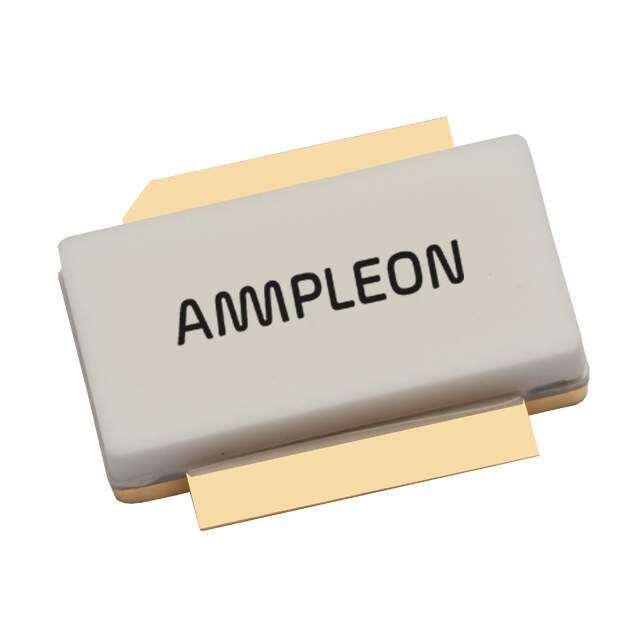
| 产品图片 |
|
| rohs | RoHS 合规性豁免无铅 / 符合限制有害物质指令(RoHS)规范要求 |
| 产品系列 | 晶体管,晶体管射频,射频MOSFET晶体管,Freescale Semiconductor AFT05MS031NR1- |
| 数据手册 | |
| 产品型号 | AFT05MS031NR1 |
| Pd-PowerDissipation | 294 W |
| Pd-功率耗散 | 294 W |
| Vds-Drain-SourceBreakdownVoltage | - 0.5 V, + 40 V |
| Vds-漏源极击穿电压 | - 0.5 V, + 40 V |
| Vgs-Gate-SourceBreakdownVoltage | - 6 V, + 12 V |
| Vgs-栅源极击穿电压 | - 6 V, + 12 V |
| Vgsth-Gate-SourceThresholdVoltage | 2.1 VDC |
| Vgsth-栅源极阈值电压 | 2.1 VDC |
| 产品种类 | 射频MOSFET晶体管 |
| 产品类型 | RF Power Transistor |
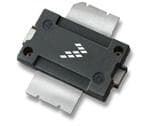
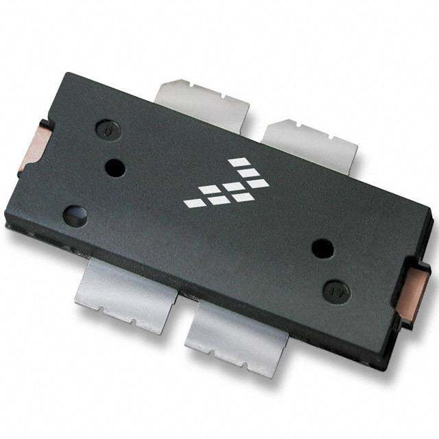
| 供应商器件封装 | TO-270-2 |
| 其它名称 | AFT05MS031NR1CT |
| 功率-输出 | 47W |
| 功率耗散 | 294 W |
| 包装 | 剪切带 (CT) |
| 单位重量 | 529.550 mg |
| 商标 | Freescale Semiconductor |
| 噪声系数 | - |
| 增益 | 17.7dB |
| 安装风格 | SMD/SMT |
| 封装 | Reel |
| 封装/外壳 | TO-270AA |
| 封装/箱体 | TO-270-2 |
| 工厂包装数量 | 500 |
| 技术 | LDMOS |
| 晶体管极性 | N-Channel |
| 晶体管类型 | LDMOS |
| 最大工作温度 | + 150 C |
| 最小工作温度 | - 40 C |
| 标准包装 | 1 |
| 正向跨导-最小值 | 5.8 S |
| 汲极/源极击穿电压 | - 0.5 V, + 40 V |
| 电压-测试 | 13.6V |
| 电压-额定 | 40V |
| 电流-测试 | 10mA |
| 类型 | LDMOS |
| 系列 | AFT05MS031N |
| 输出功率 | 33 W |
| 配置 | Single |
| 闸/源击穿电压 | - 6 V, + 12 V |
| 频率 | 520MHz |
| 额定电流 | - |


- 商务部:美国ITC正式对集成电路等产品启动337调查
- 曝三星4nm工艺存在良率问题 高通将骁龙8 Gen1或转产台积电
- 太阳诱电将投资9.5亿元在常州建新厂生产MLCC 预计2023年完工
- 英特尔发布欧洲新工厂建设计划 深化IDM 2.0 战略
- 台积电先进制程称霸业界 有大客户加持明年业绩稳了
- 达到5530亿美元!SIA预计今年全球半导体销售额将创下新高
- 英特尔拟将自动驾驶子公司Mobileye上市 估值或超500亿美元
- 三星加码芯片和SET,合并消费电子和移动部门,撤换高东真等 CEO
- 三星电子宣布重大人事变动 还合并消费电子和移动部门
- 海关总署:前11个月进口集成电路产品价值2.52万亿元 增长14.8%


PDF Datasheet 数据手册内容提取
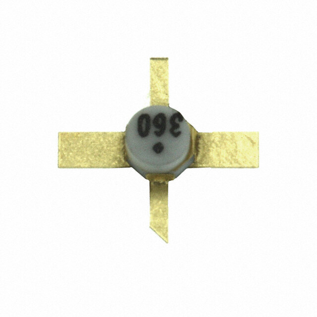
Freescale Semiconductor DocumentNumber:AFT05MS031N Technical Data Rev.1,4/2013 RF Power LDMOS Transistors High Ruggedness N--Channel AFT05MS031NR1 Enhancement--Mode Lateral MOSFETs AFT05MS031GNR1 Designedformobiletwo--wayradioapplicationswithfrequenciesfrom 136to520MHz.Thehighgain,ruggednessandbroadbandperformanceof thesedevicesmakethemidealforlarge--signal,commonsourceamplifier applicationsinmobileradioequipment. 136--520MHz,31W,13.6V TypicalPerformance:(13.6Vdc,TA=25C,CW) WIDEBAND RFPOWERLDMOSTRANSISTORS Frequency Gps D P1dB (MHz) (dB) (%) (W) 136--174(1,4) 23.2 62.0 31 380--450(2,4) 18.3 64.1 31 450--520(3,4) 17.7 62.0 31 TO--270--2 520(5) 17.7 71.4 33 PLASTIC AFT05MS031NR1 LoadMismatch/Ruggedness Frequency Signal Pin Test (MHz) Type VSWR (W) Voltage Result 155(1) CW >65:1atall 0.55 17 NoDevice PhaseAngles (3dBOverdrive) Degradation TO--270--2GULL 420(2) 1.6 PLASTIC (3dBOverdrive) AFT05MS031GNR1 490(3) 2.0 (3dBOverdrive) 520(5) 1.1 (3dBOverdrive) 1. Measuredin136--174MHzVHFbroadbandreferencecircuit. 2. Measuredin380--450MHzUHFbroadbandreferencecircuit. 3. Measuredin450--520MHzUHFbroadbandreferencecircuit. Gate Drain 4. The values shown are the minimum measured performance numbers across the indicatedfrequencyrange. 5. Measuredin520MHznarrowbandtestcircuit. Features CharacterizedforOperationfrom136to520MHz (TopView) UnmatchedInputandOutputAllowingWideFrequencyRangeUtilization Note: The backside of the package is the IntegratedESDProtection sourceterminalforthetransistor. IntegratedStabilityEnhancements Wideband—FullPowerAcrosstheBand: Figure1.PinConnections 136--174MHz 380--450MHz 450--520MHz 225CCapablePlasticPackage ExceptionalThermalPerformance HighLinearityfor:TETRA,SSB,LTE Cost--effectiveOver--moldedPlasticPackaging InTapeandReel.R1Suffix=500Units,24mmTapeWidth,13inchReel. TypicalApplications OutputStageVHFBandMobileRadio OutputStageUHFBandMobileRadio FreescaleSemiconductor,Inc.,2012--2013.Allrightsreserved. AFT05MS031NR1AFT05MS031GNR1 RFDeviceData FreescaleSemiconductor,Inc. 1
Table1.MaximumRatings Rating Symbol Value Unit Drain--SourceVoltage VDSS --0.5,+40 Vdc Gate--SourceVoltage VGS --6.0,+12 Vdc OperatingVoltage VDD 17,+0 Vdc StorageTemperatureRange Tstg --65to+150 C CaseOperatingTemperatureRange TC --40to+150 C OperatingJunctionTemperatureRange(1,2) TJ --40to+225 C TotalDeviceDissipation@TC=25C PD 294 W Derateabove25C 1.47 W/C Table2.ThermalCharacteristics Characteristic Symbol Value(2,3) Unit ThermalResistance,JunctiontoCase RJC 0.67 C/W CaseTemperature79C,31WCW,13.6Vdc,IDQ=10mA,520MHz Table3.ESDProtectionCharacteristics TestMethodology Class HumanBodyModel(perJESD22--A114) 2,passes2500V MachineModel(perEIA/JESD22--A115) A,passes100V ChargeDeviceModel(perJESD22--C101) IV,passes2000V Table4.MoistureSensitivityLevel TestMethodology Rating PackagePeakTemperature Unit PerJESD22--A113,IPC/JEDECJ--STD--020 3 260 C Table5.ElectricalCharacteristics(TA=25Cunlessotherwisenoted) Characteristic Symbol Min Typ Max Unit OffCharacteristics ZeroGateVoltageDrainLeakageCurrent IDSS — — 2 Adc (VDS=40Vdc,VGS=0Vdc) ZeroGateVoltageDrainLeakageCurrent IDSS — — 1 Adc (VDS=13.6Vdc,VGS=0Vdc) Gate--SourceLeakageCurrent IGSS — — 600 nAdc (VGS=5Vdc,VDS=0Vdc) OnCharacteristics GateThresholdVoltage VGS(th) 1.6 2.1 2.6 Vdc (VDS=10Vdc,ID=115Adc) Drain--SourceOn--Voltage VDS(on) — 0.13 — Vdc (VGS=10Vdc,ID=1.2Adc) ForwardTransconductance gfs — 5.8 — S (VDS=10Vdc,ID=7.5Adc) 1. ContinuoususeatmaximumtemperaturewillaffectMTTF. 2. MTTFcalculatoravailableathttp://www.freescale.com/rf.SelectSoftware&Tools/DevelopmentTools/CalculatorstoaccessMTTF calculatorsbyproduct. 3. RefertoAN1955,ThermalMeasurementMethodologyofRFPowerAmplifiers.Gotohttp://www.freescale.com/rf. SelectDocumentation/ApplicationNotes--AN1955. (continued) AFT05MS031NR1AFT05MS031GNR1 RFDeviceData 2 FreescaleSemiconductor,Inc.
Table5.ElectricalCharacteristics(TA=25Cunlessotherwisenoted)(continued) Characteristic Symbol Min Typ Max Unit DynamicCharacteristics ReverseTransferCapacitance Crss — 1.6 — pF (VDS=13.6Vdc30mV(rms)ac@1MHz,VGS=0Vdc) OutputCapacitance Coss — 49.5 — pF (VDS=13.6Vdc30mV(rms)ac@1MHz,VGS=0Vdc) InputCapacitance Ciss — 109 — pF (VDS=13.6Vdc,VGS=0Vdc30mV(rms)ac@1MHz) FunctionalTests(1)(InFreescaleNarrowbandTestFixture,50ohmsystem)VDD=13.6Vdc,IDQ=10mA,Pout=31W,f=520MHz Common--SourceAmplifierPowerGain Gps 16.5 17.7 19.0 dB DrainEfficiency D 70.0 71.4 — % LoadMismatch/Ruggedness(InFreescaleTestFixture,50ohmsystem)IDQ=10mA Frequency Signal Pin (MHz) Type VSWR (W) TestVoltage,VDD Result 520 CW >65:1atallPhaseAngles 1.1 17 NoDeviceDegradation (3dBOverdrive) 1. Measurementsmadewithdeviceinstraightleadconfigurationbeforeanyleadformingoperationisapplied.Leadformingisusedforgull wing(GN)parts. AFT05MS031NR1AFT05MS031GNR1 RFDeviceData FreescaleSemiconductor,Inc. 3
TYPICALCHARACTERISTICS 1000 7 Measuredwith30mV(rms)ac@1MHz,VGS=0Vdc 6 TA=25C VGS=4.25Vdc S) P M (pF) 100 Ciss T(A 5 4Vdc CE Coss EN 4 AN RR 3.75Vdc T U ACI NC 3 AP AI 3.5Vdc C 10 R C, ,DS 2 ID 3.25Vdc 1 Crss 2.75Vdc 3Vdc 1 0 0 4 8 12 16 20 0 4 8 12 16 20 VDS,DRAIN--SOURCEVOLTAGE(VOLTS) VDS,DRAIN--SOURCEVOLTAGE(VOLTS) Figure2.CapacitanceversusDrain--SourceVoltage Figure3.DrainCurrentversusDrain--SourceVoltage 109 108 VDD=13.6Vdc ID=2.5Amps S) 107 3.2Amps R U O H ( TF 106 T M 3.9Amps 105 104 90 110 130 150 170 190 210 230 250 TJ,JUNCTIONTEMPERATURE(C) Note:MTTFvaluerepresentsthetotalcumulativeoperatingtime underindicatedtestconditions. MTTFcalculatoravailableathttp://www.freescale.com/rf.Select Software&Tools/DevelopmentTools/CalculatorstoaccessMTTF calculatorsbyproduct. Figure4.MTTFversusJunctionTemperature--CW AFT05MS031NR1AFT05MS031GNR1 RFDeviceData 4 FreescaleSemiconductor,Inc.
520MHzNARROWBANDPRODUCTIONTESTFIXTURE C1 C7 C13 C14 B3 C16 B2 C3 B1 C2 C4 C8 C18 C5 C9 L2 C11 L1 C15 A E C6 C10 R A C12 T U O T U C C17 AFT05MS031N Rev.1 Figure5.AFT05MS031NR1NarrowbandTestCircuitComponentLayout—520MHz Table6.AFT05MS031NR1NarrowbandTestCircuitComponentDesignationsandValues—520MHz Part Description PartNumber Manufacturer B1,B2,B3 RFBeads,Long 2743021447 Fair--Rite C1 22F,35VTantalumCapacitor T491X226K035AT Kemet C2,C14 0.01FChipCapacitors C0805C103K5RAC Kemet C3,C13 0.1FChipCapacitors CDR33BX104AKWS Kemet C4 200pFChipCapacitor ATC100B201JT300XT ATC C5 6.2pFChipCapacitor ATC100B6R2JT500XT ATC C6 3.9pFChipCapacitor ATC100B3R9JT500XT ATC C7,C16 180pFChipCapacitors ATC100B181JT200XT ATC C8 10pFChipCapacitor ATC100B100JT500XT ATC C9,C10,C11,C12 36pFChipCapacitors ATC100B360JT500XT ATC C15 27pFChipCapacitor ATC100B270JT500XT ATC C17 7.5pFChipCapacitor ATC100B7R5JT500XT ATC C18 470F,63VElectrolyticCapacitor SME63V471M12X25LL UnitedChemi--Con L1 43nH,10TurnInductor B10TJLC Coilcraft L2 56nHInductor 1812SMS--56NJLC Coilcraft PCB 0.030,r=2.55 AD255A Arlon AFT05MS031NR1AFT05MS031GNR1 RFDeviceData FreescaleSemiconductor,Inc. 5
T U FP RT U O 4 S 1 D Z V 1 1 C + C18 Z13 7 1 C 4 1 z C H C16C13 L2 Z10Z12Z11 C12C15 cuitSchematic—520M Microstrips—520MHz Description 0.1900.270Microstrip 0.2570.275Microstrip 0.1450.275Microstrip 0.0910.082Microstrip 0.13220.082Microstrip 0.14200.082Microstrip 0.3150.082Microstrip 9 Cir uit p Z ndTest estCirc Microstri Z8 Z9 Z10 Z11 Z12* Z13* Z14 9 a T C Z8 owb and L1 C8 Z7Z6 C10 S031NR1Narr NR1Narrowb scription 082Microstrip 082Microstrip 082Microstrip 060Microstrip 082Microstrip 082Microstrip 082Microstrip crostripbends M 31 De 0. 0. 0. 0. 0. 0. 0. mi Z5 05 S0 es C7 Z4 AFT 05M 0.199 0.017 0.670 0.560 0.370 0.079 0.352 nclud C3C4 Z3Z2 C6 Figure6. Table7.AFT Microstrip Z1 Z2 Z3* Z4* Z5* Z6 Z7 *Linelengthi 2 5 C C + C1 Z1 T FU RP N S I G V AFT05MS031NR1AFT05MS031GNR1 RFDeviceData 6 FreescaleSemiconductor,Inc.
TYPICALCHARACTERISTICS—520MHz 50 45 VDD=13.6Vdc,Pin=0.6W S) 40 VDD=13.6Vdc,Pin=0.3W T WAT 35 VDD=12.5Vdc,Pin=0.6W ( R 30 E W O 25 P T U 20 UTP 15 VDD=12.5Vdc O Pin=0.3W P,out 10 5 f=520MHz 0 0 1 2 3 4 5 6 VGS,GATE--SOURCEVOLTAGE(VOLTS) Figure7.OutputPowerversusGate--SourceVoltage 20 90 19 VDD=13.6Vdc,IDQ=10mA 80 f=520MHz D 18 70 S) ERGAIN(dB) 111765 Gps 465000 POWER(WATT FFICIENCY(%) W T E G,POps 14 Pout 30 OUTPU DRAIN 13 20 P,out ,D 12 10 11 0 0.03 0.1 1 3 Pin,INPUTPOWER(WATTS) Figure8.PowerGain,OutputPowerandDrain EfficiencyversusInputPower VDD=13.6Vdc,IDQ=10mA,Pout=31WAvg. f Zsource Zload MHz 520 0.72+j1.77 1.54+j0.80 Zsource = Testcircuitimpedanceasmeasuredfrom gatetoground. Zload = Testcircuitimpedanceasmeasuredfrom draintoground. Input Device Output Matching Under Matching Network Test Network 50 50 Zsource Zload Figure9.NarrowbandSeriesEquivalentSourceandLoadImpedance—520MHz AFT05MS031NR1AFT05MS031GNR1 RFDeviceData FreescaleSemiconductor,Inc. 7
136--174MHzVHFBROADBANDREFERENCECIRCUIT Table8.136--174MHzVHFBroadbandPerformance(InFreescaleReferenceCircuit,50ohmsystem) VDD=13.6Volts,IDQ=100mA,TA=25C,CW Frequency Gps D P1dB (MHz) (dB) (%) (W) 136 25.0 64.0 31 155 23.2 63.0 31 174 23.2 62.0 31 Table9.LoadMismatch/Ruggedness(InFreescaleReferenceCircuit) Frequency Signal Pin (MHz) Type VSWR (W) TestVoltage,VDD Result 155 CW >65:1atall 0.55 17 NoDevice PhaseAngles (3dBOverdrive) Degradation AFT05MS031NR1AFT05MS031GNR1 RFDeviceData 8 FreescaleSemiconductor,Inc.
136--174MHzVHFBROADBANDREFERENCECIRCUIT C1 C16 C17 B2 B1 C14 C11 C12 C13 C15 J1 C2 C10 5 1 L1 75 3 D R1 L3 L6 C3 C6 C7 Q1 C4 L5 C5 L4 R2 L2 C8 C9 Figure10.AFT05MS031NR1VHFBroadbandReferenceCircuitComponentLayout—136--174MHz Table10.AFT05MS031NR1VHFBroadbandReferenceCircuitComponentDesignationsandValues—136--174MHz Part Description PartNumber Manufacturer B1 LowCurrentFerriteBead 2508051107Y0 Fair-Rite B2 HighCurrentFerriteBead 2518065007Y6 Fair-Rite C1 68pFChipCapacitor ATC600F680JT250XT ATC C2 47pFChipCapacitor ATC600F470BT250XT ATC C3,C4,C6,C7 100pFChipCapacitors ATC600F101JT250XT ATC C5 20pFChipCapacitor ATC600F200JT250XT ATC C8,C9 56pFChipCapacitors ATC600F560JT250XT ATC C10 27pFChipCapacitor ATC600F270JT250XT ATC C11 0.1FChipCapacitor GRM21BR71H104KA01B Murata C12 1FChipCapacitor GRM21BR71H105KA12L Murata C13,C14,C15 240pFChipCapacitors ATC600F241JT250XT ATC C16,C17 10FChipCapacitors GRM31CR61H106KA12L Murata J1 3PinConnector AMP-9-146305-0 TEConnectivity L1 19nHInductor 0806SQ--19NGLC Coilcraft L2 6.9nHInductor 0807SQ--6N9GLC Coilcraft L3 27nHInductor 0908SQ--27NGLC Coilcraft L4 6nHInductor 0806SQ--6N0GLC Coilcraft L5 14nHInductor 0807SQ--14NGLC Coilcraft L6 10nHInductor 0807SQ--10NGLC Coilcraft Q1 RFPowerLDMOSTransistor AFT05MS031NR1 Freescale R1 62,1/4WChipResistor RG2012N-620-BT1 Susumu R2 0,1/4WChipResistor CWCR08050000Z0EA Vishay PCB 0.020,r=4.9 S1000-2 Shengyi AFT05MS031NR1AFT05MS031GNR1 RFDeviceData FreescaleSemiconductor,Inc. 9
T U FP RT U O 2 2 Z 2 1 C 1 Z2 11 C 0 2 Z p p p p p p p p L6 on crostri crostri crostri crostri crostri crostri crostri crostri Z19 L5 Descripti 0.230Mi 0.200Mi 0.190Mi 0.050Mi 0.150Mi 0.060Mi 0.130Mi 0.080Mi Z18 C10 034 034 034 034 034 034 034 034 0. 0. 0. 0. 0. 0. 0. 0. VDS C15 Z17 4 C9 6--174MHz Microstrip Z17 Z18 Z19 Z20 Z21 Z22 Z23 Z24 L z 3 H 1 14 6 M — C13CC17 B2 L3 Z14Z15Z1 C7C8 atic—136--174 uitMicrostrips Description 0.170Microstrip 0.130Microstrip 0.080Microstrip 0.155Microstrip 0.115Microstrip 0.050Microstrip 0.065Microstrip 0.140Microstrip m c Z24 Z23 Z13 C6 Sche ceCir 0.240 0.034 0.034 0.240 0.240 0.240 0.034 0.034 Z12 Circuit Referen ostrip nce nd Micr Z9 Z10 Z11 Z12 Z13 Z14 Z15 Z16 B1 R1 Z9 ere dba Z11 Z10 Z8 ndRef FBroa strip strip strip strip strip strip strip strip C16C5 Z7 R2 Broadba NR1VH cription 60Micro 20Micro 57Micro 20Micro 75Micro 31Micro 09Micro 20Micro 1 s 0 1 0 1 0 4 3 0 VGS Z6 L2 NR1VHF T05MS03 De 0.0340. 0.0340. 0.0340. 0.0340. 0.0340. 0.0340. 0.0340. 0.2400. 5 1 F Z C4 03 A p Z4 C3 AFT05MS Table11. Microstri Z1 Z2 Z3 Z4 Z5 Z6 Z7 Z8 1. L1 1 e r u Z3 2 g C Fi 2 Z 1 C 1 Z T FU RP N I AFT05MS031NR1AFT05MS031GNR1 RFDeviceData 10 FreescaleSemiconductor,Inc.
TYPICALCHARACTERISTICS—136--174MHzVHFBROADBAND REFERENCECIRCUIT 22.6 76 22.5 VDD=12.5Vdc,Pin=0.2W(Avg.) 74 IDQ=100mA %) (dB) 2222..43 7720 DRAINENCY( AIN 22.2 68 ,DFICI RG 22.1 D 66 EF E W PO 22 Gps 64 G,ps21.9 36 UTTTS) 21.8 33 PA TW 2211..67 Pout 3207 P,OUoutOWER( P 130 140 150 160 170 180 f,FREQUENCY(MHz) Figure12.PowerGain,DrainEfficiencyandOutputPowerversus FrequencyataConstantInputPower—12.5V 23.1 74 23 VDD=13.6Vdc,Pin=0.2W(Avg.) 72 IDQ=100mA %) B) 2222..98 7608 RAINNCY( GAIN(d 22.7 D 66 ,DDFFICIE R 22.6 64 E E W O 22.5 Gps 62 P G,ps22.4 39 UTTTS) 22.3 36 PA TW 22.2 Pout 33 OUR( 22.1 30 P,outOWE P 130 140 150 160 170 180 f,FREQUENCY(MHz) Figure13.PowerGain,DrainEfficiencyandOutputPowerversus FrequencyataConstantInputPower—13.6V AFT05MS031NR1AFT05MS031GNR1 RFDeviceData FreescaleSemiconductor,Inc. 11
TYPICALCHARACTERISTICS—136--174MHzVHFBROADBAND REFERENCECIRCUIT 50 VDD=13.6Vdc,Pin=0.2W 25 S) 40 TS) VDD=13.6Vdc TT VDD=13.6Vdc,Pin=0.1W AT 20 Pin=0.2W A W W ( ER( 30 VDD=12.5Vdc,Pin=0.2W VDD=12.5Vdc WER 15 VDD=12.5Vdc OW Pin=0.1W PO Pin=0.2W VDD=12.5Vdc TP UT 10 Pin=0.1W U 20 P P T UT DetailA OU VDD=13.6Vdc P,Oout 10 P,out 5 Pin=0.f1=W155MHz f=155MHz 0 0 0.5 1 1.5 2 2.5 3 3.5 0 0 1 2 3 4 5 VGS,GATE--SOURCEVOLTAGE(VOLTS) VGS,GATE--SOURCEVOLTAGE(VOLTS) DetailA Figure14.OutputPowerversusGate--SourceVoltage 27 140 80 VDD=13.6Vdc,IDQ=100mA D 26 136MHz 155MHz 120 70 174MHz S) RGAIN(dB) 2245 136MHz 81000 WER(WATT 5600 CIENCY(%) WE 23 60 PO 40 FFI PO Gps 155MHz UT NE G,ps 2221 174MHz Pout 136MHz 4200 P,OUTPout 3200 ,DRAID 174MHz 155MHz 20 10 10 0.01 0.1 0.5 Pin,INPUTPOWER(WATTS) Figure15.PowerGain,OutputPowerandDrain EfficiencyversusInputPowerandFrequency AFT05MS031NR1AFT05MS031GNR1 RFDeviceData 12 FreescaleSemiconductor,Inc.
136--174MHzVHFBROADBANDREFERENCECIRCUIT Zsource Zo=5 f=135MHz f=175MHz f=175MHz Zload f=135MHz VDD=13.6Vdc,IDQ=100mA,Pout=31WAvg. f Zsource Zload MHz 135 3.33+j6.92 2.42-j0.95 140 3.66+j7.23 2.59-j0.96 145 3.97+j7.44 2.71-j1.03 150 4.21+j7.53 2.78-j1.13 155 4.31+j7.54 2.77-j1.23 160 4.21+j7.54 2.71-j1.31 165 3.94+j7.65 2.61-j1.34 170 3.58+j7.94 2.50-j1.32 175 3.24+j8.42 2.41-j1.24 Zsource = Testcircuitimpedanceasmeasuredfrom gatetoground. Zload = Testcircuitimpedanceasmeasuredfrom draintoground. Input Device Output Matching Under Matching Network Test Network 50 50 Zsource Zload Figure16.VHFBroadbandSeriesEquivalentSourceandLoadImpedance—136--174MHz AFT05MS031NR1AFT05MS031GNR1 RFDeviceData FreescaleSemiconductor,Inc. 13
380--450MHzUHFBROADBANDREFERENCECIRCUIT Table12.380--450MHzUHFBroadbandPerformance(InFreescaleReferenceCircuit,50ohmsystem) VDD=13.6Volts,IDQ=100mA,TA=25C,CW Frequency Gps D P1dB (MHz) (dB) (%) (W) 380 18.7 64.1 31 420 18.6 67.0 31 450 18.3 68.1 31 Table13.LoadMismatch/Ruggedness(InFreescaleReferenceCircuit) Frequency Signal Pin (MHz) Type VSWR (W) TestVoltage,VDD Result 420 CW >65:1atall 1.6 17 NoDevice PhaseAngles (3dBOverdrive) Degradation AFT05MS031NR1AFT05MS031GNR1 RFDeviceData 14 FreescaleSemiconductor,Inc.
380--450MHzUHFBROADBANDREFERENCECIRCUIT VGS VDS C1 B1 C13 C14 C15 B2 C12 C17 J1 C16 C6 C11 5 1 5 7 3 D L1 R1 L7 C5* C10 L4 C8 C2 Q1 L6 C7 C4* L2 L3 L5 C3 C9 *C4andC5aremountedvertically. Figure17.AFT05MS031NR1UHFBroadbandReferenceCircuitComponentLayout—380--450MHz Table14.AFT05MS031NR1UHFBroadbandReferenceCircuitComponentDesignationsandValues—380--450MHz Part Description PartNumber Manufacturer B1 LowCurrentFerriteBead 2508051107Y0 Fair--Rite B2 HighCurrentFerriteBead 2518065007Y6 Fair--Rite C1,C5 56pFChipCapacitors ATC600F560JT250XT ATC C2 3.9pFChipCapacitor ATC600F3R9BT250XT ATC C3 18pFChipCapacitor ATC600F180JT250XT ATC C4 47pFChipCapacitor ATC600F470JT250XT ATC C6,C12,C15 240pFChipCapacitors ATC600F241JT250XT ATC C7 24pFChipCapacitor ATC600F240JT250XT ATC C8 68pFChipCapacitor ATC600F680JT250XT ATC C9 27pFChipCapacitor ATC600F270JT250XT ATC C10 8.2pFChipCapacitor ATC600F8R2BT250XT ATC C11 3.0pFChipCapacitor ATC600F3R0BT250XT ATC C13 0.1FChipCapacitor GRM21BR71H104KA01B Murata C14 1FChipCapacitor GRM21BR71H105KA12L Murata C16,C17 10FChipCapacitors GRM31CR61H106KA12L Murata J1 3PinConnector AMP--9--146305--0 TEConnectivity L1,L2,L3,L6 5.5nHInductors 0806SQ--5N5GLC Coilcraft L4 17nHInductor 0908SQ--17NGLC Coilcraft L5 1.65nHInductor 0906--2KLC Coilcraft L7 2.55nHInductor 0906--3JLC Coilcraft Q1 RFPowerLDMOSTransistor AFT05MS031NR1 Freescale R1 62,1/4WChipResistor RG2012N--620--BT1 Susumu PCB 0.020,r=4.9 S1000--2 Shengyi AFT05MS031NR1AFT05MS031GNR1 RFDeviceData FreescaleSemiconductor,Inc. 15
T U FP RT U O 7 2 Z 2 1 C Z26 C11 5 2 Z 7 L Z24 C10 p p p p p p p p p stri stri stri stri stri stri stri stri stri DS Z23 L6 MHz cription 57Micro 01Micro 10Micro 61Micro 12Micro 83Micro 73Micro 77Micro 60Micro V s 0 2 1 3 1 0 0 0 0 Z22 C9 450 De 0. 0. 0. 0. 0. 0. 0. 0. 0. C16 21 80-- 034 034 034 034 034 034 034 034 034 Z 3 0. 0. 0. 0. 0. 0. 0. 0. 0. 3 — C14C115 Z19Z20 L5 C8 Schematic 80--450MHz Microstrip Z19 Z20* Z21* Z22* Z23 Z24 Z25 Z26 Z27 C Z17 B2 L4 Z18 cuit —3 Z16 Z15Z14 C7 dReferenceCir cuitMicrostrips Description 0.048Microstrip 0.142Microstrip 0.149Microstrip 0.085Microstrip 0.090Microstrip 0.186Microstrip 0.149Microstrip 0.085Microstrip 0.044Microstrip B1 R1 Z11 ban Cir 40 40 34 34 40 40 34 34 40 d e 2 2 0 0 2 2 0 0 2 3 2 10 oa nc 0. 0. 0. 0. 0. 0. 0. 0. 0. 1 1 Z r e Z Z B r p C6 Z9 C5 HF Refe ostri C17 Z8 C4 NR1U band Micr Z10 Z11 Z12 Z13* Z14 Z15 Z16 Z17* Z18 1 d 3 a 0 o VGS Z6Z7 L3 C3 18.AFT05MS 1NR1UHFBr scription 060Microstrip 200Microstrip 056Microstrip 154Microstrip 237Microstrip 234Microstrip 010Microstrip 083Microstrip 178Microstrip crostripbends re 03 De 0. 0. 0. 0. 0. 0. 0. 0. 0. mi Z5 gu MS es Fi 5 34 34 34 34 34 34 34 34 34 ud L2 FT0 0.0 0.0 0.0 0.0 0.0 0.0 0.0 0.0 0.0 incl A p gth Z4 C2 15. stri len Z3 Table Micro Z1 Z2 Z3 Z4 Z5* Z6* Z7 Z8 Z9 *Line 1 L 2 Z 1 C 1 Z T FU RP N I AFT05MS031NR1AFT05MS031GNR1 RFDeviceData 16 FreescaleSemiconductor,Inc.
TYPICALCHARACTERISTICS—380--450MHzUHFBROADBAND REFERENCECIRCUIT 18 80 %) 1177..98 VIDDQD==11020.5mVAdc,Pin=0.5W(Avg.) D 7750 DRAINENCY( GAIN(dB) 1177..76 Gps 6605 ,DEFFICI R 17.5 30 E G,POWps11117777....4321 Pout 22226987 P,OUTPUToutPOWER(WATTS) 17 25 370 380 390 400 410 420 430 440 450 460 f,FREQUENCY(MHz) Figure19.PowerGain,DrainEfficiencyandOutputPowerversus FrequencyataConstantInputPower—12.5V 18.5 80 18.4 VIDDQD==11030.6mVAdc,Pin=0.5W(Avg.) 75 AINCY(%) 18.3 D 70 DREN AIN(dB) 1188..21 Gps 6650 ,DEFFICI G R 18 35 E POW 17.9 34 UTTTS) G,ps111777...876 Pout 333321 P,OUTPoutPOWER(WA 17.5 30 370 380 390 400 410 420 430 440 450 460 f,FREQUENCY(MHz) Figure20.PowerGain,DrainEffiencyandOutputPowerversus FrequencyataConstantInputPower—13.6V AFT05MS031NR1AFT05MS031GNR1 RFDeviceData FreescaleSemiconductor,Inc. 17
TYPICALCHARACTERISTICS—380--450MHzUHFBROADBAND REFERENCECIRCUIT 50 VDD=13.6Vdc,Pin=0.5W 5 TTS) 40 VDD=13.6Vdc,Pin=0.25W ATTS) 4 PVDinD==01.53.W6Vdc, VDD=13.6Vdc,Pin=0.25W A W W VDD=12.5Vdc,Pin=0.5W ( ( R WER 30 OWE 3 VDD=12.5Vdc, TPUTPO 20 PVDinD==01.225.5WVdc, UTPUTP 2 Pin=0.5W VDD=12.5Vdc, OU O 1 Pin=0.25W P,out 10 f=420MHz P,out f=420MHz 0 DetailA 0 0.4 0.8 1.2 1.6 2 0 0 1 2 3 4 5 VGS,GATE--SOURCEVOLTAGE(VOLTS) VGS,GATE--SOURCEVOLTAGE(VOLTS) DetailA Figure21.OutputPowerversusGate--SourceVoltage 22 100 80 VDD=13.6Vdc,IDQ=100mA 420MHz 70 20 80 GAIN(dB) 18 45042M0HMzHz 3804M42H500zMMHHzz 60 ER(WATTS) 5600 ENCY(%) OWER 16 Gps 380MHz 450MHz 40 TPOW 40 EFFICI P U N G,ps 380MHz OUTP 30 DRAI 14 D Pout 20 P,out 20 ,D 12 0 10 0.01 0.1 1 4 Pin,INPUTPOWER(WATTS) Figure22.PowerGain,OutputPowerandDrain EfficiencyversusInputPowerandFrequency AFT05MS031NR1AFT05MS031GNR1 RFDeviceData 18 FreescaleSemiconductor,Inc.
380--450MHzUHFBROADBANDREFERENCECIRCUIT f=450MHz Zo=5 f=380MHz Zsource f=380MHz f=450MHz Zload VDD=13.6Vdc,IDQ=100mA,Pout=31WAvg. f Zsource Zload MHz 380 1.57+j1.94 2.53--j0.27 390 1.66+j2.07 2.53--j0.26 400 1.74+j2.16 2.56--j0.27 410 1.79+j2.20 2.49--j0.29 420 1.79+j2.21 2.38--j0.28 430 1.74+j2.21 2.26--j0.24 440 1.62+j2.23 2.11--j0.16 450 1.45+j2.29 1.95--j0.05 Zsource = Testcircuitimpedanceasmeasuredfrom gatetoground. Zload = Testcircuitimpedanceasmeasuredfrom draintoground. Input Device Output Matching Under Matching Network Test Network 50 50 Zsource Zload Figure23.UHFBroadbandSeriesEquivalentSourceandLoadImpedance—380--450MHz AFT05MS031NR1AFT05MS031GNR1 RFDeviceData FreescaleSemiconductor,Inc. 19
450--520MHzUHFBROADBANDREFERENCECIRCUIT Table16.450--520MHzUHFBroadbandPerformance(InFreescaleReferenceCircuit,50ohmsystem) VDD=13.6Volts,IDQ=100mA,TA=25C,CW Frequency Gps D P1dB (MHz) (dB) (%) (W) 450 17.7 62.0 31 490 18.7 63.8 31 520 17.9 67.0 31 Table17.LoadMismatch/Ruggedness(InFreescaleReferenceCircuit) Frequency Signal Pin (MHz) Type VSWR (W) TestVoltage,VDD Result 490 CW >65:1atall 2.0 17 NoDevice PhaseAngles (3dBOverdrive) Degradation AFT05MS031NR1AFT05MS031GNR1 RFDeviceData 20 FreescaleSemiconductor,Inc.
450--520MHzUHFBROADBANDREFERENCECIRCUIT VGS VDS C1 B1 C13 C14 C15 B2 C17 C19 J1 C18 C16 C12 5 1 5 7 3 D L1 R1 L7 C5 C6 L4 C9 C11 Q1 C8 C2 C4 C7 L2 L6 L3 L5 C3 C10 Figure24.AFT05MS031NR1UHFBroadbandReferenceCircuitComponentLayout—450--520MHz Table18.AFT05MS031NR1UHFBroadbandReferenceCircuitComponentDesignationsandValues—450--520MHz Part Description PartNumber Manufacturer B1 LowCurrentFerriteBead 2508051107Y0 Fair--Rite B2 HighCurrentFerriteBead 2518065007Y6 Fair--Rite C1 56pFChipCapacitor ATC600F560JT250XT ATC C2 2.7pFChipCapacitor ATC600F2R7BT250XT ATC C3 12pFChipCapacitor ATC600F120JT250XT ATC C4,C9 27pFChipCapacitors ATC600F270JT250XT ATC C5,C8 33pFChipCapacitors ATC600F330JT250XT ATC C6 39pFChipCapacitor ATC600F390JT250XT ATC C7,C10 18pFChipCapacitors ATC600F180JT250XT ATC C11 8.2pFChipCapacitor ATC600F8R2BT250XT ATC C12 1.8pFChipCapacitor ATC600F1R8BT250XT ATC C13 0.1FChipCapacitor GRM21BR71H104KA01B Murata C14 1FChipCapacitor GRM21BR71H105KA12L Murata C15,C16,C17 240pFChipCapacitors ATC600F241JT250XT ATC C18,C19 10FChipCapacitors GRM31CR61H106KA12L Murata J1 3PinConnector AMP--9--146305--0 TEConnectivity L1,L3 6.0nHInductors 0806SQ--6N0GLC Coilcraft L2,L6 5.5nHInductors 0806SQ5N5GLC Coilcraft L4 17nHInductor 0908SQ--17NGLC Coilcraft L5,L7 1.65nHInductors 0906--2KLC Coilcraft Q1 RFPowerLDMOSTransistor AFT05MS031NR1 Freescale R1 62,1/4WChipResistor RG2012N--620--BT1 Susumu PCB 0.020,r=4.9 S1000--2 Shengyi AFT05MS031NR1AFT05MS031GNR1 RFDeviceData FreescaleSemiconductor,Inc. 21
T U FP RT U O 29 Z 7 1 C Z28 C12 7 2 Z 7 L Z26 C11 p p p* p* p p p p p Z25 ostri ostri ostri ostri ostri ostri ostri ostri ostri VDS Z24 L6 C10 20MHz Description 0.010Micr 0.176Micr 0.118Micr 0.295Micr 0.018Micr 0.177Micr 0.022Micr 0.188Micr 0.060Micr 5 C18 Z23 L5 —450-- 0.034 0.034 0.034 0.034 0.034 0.034 0.034 0.034 0.034 C13 Z22 C9 matic 0MHz ostrip C14 Z21 C8 che --52 Micr Z21 Z22 Z23* Z24* Z25 Z26 Z27 Z28 Z29 S 0 C15 Z18 B2 Z17 L4 Z16Z19Z20Z15 C7 eferenceCircuit Microstrips—45 cription 10Microstrip 80Microstrip 49Microstrip 84Microstrip 54Microstrip 70Microstrip 49Microstrip 84Microstrip 44Microstrip 57Microstrip dR uit Des 0.0 0.1 0.1 0.0 0.0 0.1 0.1 0.1 0.0 0.0 n c Z14 B1 Z13 R1 Z11Z12 Broadba renceCir p 0.240 0.240 0.034 0.034 0.240 0.240 0.034 0.034 0.240 0.034 C16 Z10 C6 UHF Refe ostri C19 Z8Z9 C4C5 S031NR1 oadband Micr Z11 Z12 Z13 Z14 Z15 Z16 Z17 Z18 Z19 Z20 VGS Z7 T05M HFBr ostrip ostrip ostrip ostrip ostrip ostrip ostrip ostrip ostrip ostrip ends Z5Z6 L3 C3 Figure25.AF 5MS031NR1U Description 340.060Micr 340.200Micr 340.128Micr 340.054Micr 340.202Micr 340.160Micr 340.010Micr 340.115Micr 340.060Micr 340.150Micr udesmicrostripb T0 0.0 0.0 0.0 0.0 0.0 0.0 0.0 0.0 0.0 0.0 ncl L2 AF p gthi Z3Z4 C2 Table19. Microstri Z1 Z2 Z3 Z4 Z5* Z6* Z7 Z8 Z9 Z10 *Linelen 1 L 2 Z 1 C 1 Z T FU RP N I AFT05MS031NR1AFT05MS031GNR1 RFDeviceData 22 FreescaleSemiconductor,Inc.
TYPICALCHARACTERISTICS—450--520MHzUHFBROADBAND REFERENCECIRCUIT 18 70 17.8 VDD=12.5Vdc,Pin=0.5W(Avg.) D 68 %) 17.6 IDQ=100mA 66 AINCY( RN dB) 17.4 64 ,DDCIE AIN( 17.2 Gps 62 EFFI G R 17 60 E W O 16.8 30 P Pout S) G,ps16.6 29 PUTATT TW 16.4 28 OUR( 16.2 27 P,outOWE 16 26 P 440 450 460 470 480 490 500 510 520 530 f,FREQUENCY(MHz) Figure26.PowerGain,DrainEfficiencyandOutputPowerversus FrequencyataConstantInputPower—12.5V 19 73 1188.7.55 VIDDQD==11030.6mVAdc,Pin=0.5W(Avg.) 6791 AINCY(%) N(dB) 18.1285 Gps 6675 ,DRDFICIEN AI17.75 D 63 EF G R 17.5 61 E W17.25 36 G,POps16.7157 Pout 3342 TPUTWATTS) 16.5 30 OUR( 16.25 28 P,outOWE P 16 26 440 450 460 470 480 490 500 510 520 530 f,FREQUENCY(MHz) Figure27.PowerGain,DrainEfficiencyandOutputPowerversus FrequencyataConstantInputPower—13.6V AFT05MS031NR1AFT05MS031GNR1 RFDeviceData FreescaleSemiconductor,Inc. 23
TYPICALCHARACTERISTICS—450--520MHzUHFBROADBAND REFERENCECIRCUIT 60 ATTS) 50 VDDV=DD13=.613V.6dcV,dPcin,P=in0.=250.W5W WATTS)2205 PVDinD==01.53.W6Vdc, VDD=13.6Vdc,Pin=0.25W W 40 VDD=12.5Vdc,Pin=0.5W ( R( ER15 VDD=12.5Vdc, WE OW Pin=0.5W O 30 P TPUTP 20 PVDinD==01.225.5WVdc, UTPUT10 PVDinD==01.225.5WVdc, U O O 5 P,out 10 f=490MHz P,out f=490MHz 0 DetailA 0 0.5 1 1.5 2 2.5 3 3.5 0 0 1 2 3 4 5 6 VGS,GATE--SOURCEVOLTAGE(VOLTS) VGS,GATE--SOURCEVOLTAGE(VOLTS) DetailA Figure28.OutputPowerversusGate--SourceVoltage 20 80 520MHz Gps 490MHz 450MHz S) GAIN(dB) 18 490MHz 450MHz D 490MHz 60 WER(WATT CIENCY(%) R 16 40 O FI WE TP EF G,POps 14 520MHz Pout 450M5H2z0MHz 20 P,OUTPUout ,DRAIND VDD=13.6Vdc,IDQ=100mA 12 0 0.01 0.1 1 3 Pin,INPUTPOWER(WATTS) Figure29.PowerGain,OutputPowerandDrain EfficiencyversusInputPowerandFrequency AFT05MS031NR1AFT05MS031GNR1 RFDeviceData 24 FreescaleSemiconductor,Inc.
450--520MHzUHFBROADBANDREFERENCECIRCUIT f=520MHz Zo=5 f=450MHz Zsource f=520MHz f=450MHz Zload VDD=13.6Vdc,IDQ=100mA,Pout=31WAvg. f Zsource Zload MHz 450 1.37+j1.64 2.57--j1.01 460 1.43+j1.72 2.49--j1.03 470 1.47+j1.79 2.38--j1.03 480 1.49+j1.83 2.26--j1.01 490 1.47+j1.86 2.11--j0.95 500 1.41+j1.89 1.97--j0.87 510 1.32+j1.93 1.82--j0.76 520 1.20+j1.99 1.68--j0.62 Zsource = Testcircuitimpedanceasmeasuredfrom gatetoground. Zload = Testcircuitimpedanceasmeasuredfrom draintoground. Input Device Output Matching Under Matching Network Test Network 50 50 Zsource Zload Figure30.UHFBroadbandSeriesEquivalentSourceandLoadImpedance—450--520MHz AFT05MS031NR1AFT05MS031GNR1 RFDeviceData FreescaleSemiconductor,Inc. 25
PACKAGEDIMENSIONS AFT05MS031NR1AFT05MS031GNR1 RFDeviceData 26 FreescaleSemiconductor,Inc.
AFT05MS031NR1AFT05MS031GNR1 RFDeviceData FreescaleSemiconductor,Inc. 27
AFT05MS031NR1AFT05MS031GNR1 RFDeviceData 28 FreescaleSemiconductor,Inc.
AFT05MS031NR1AFT05MS031GNR1 RFDeviceData FreescaleSemiconductor,Inc. 29
AFT05MS031NR1AFT05MS031GNR1 RFDeviceData 30 FreescaleSemiconductor,Inc.
AFT05MS031NR1AFT05MS031GNR1 RFDeviceData FreescaleSemiconductor,Inc. 31
PRODUCTDOCUMENTATION,SOFTWAREANDTOOLS Refertothefollowingdocuments,softwareandtoolstoaidyourdesignprocess. ApplicationNotes AN1907:SolderReflowAttachMethodforHighPowerRFDevicesinOver--MoldedPlasticPackages AN1955:ThermalMeasurementMethodologyofRFPowerAmplifiers AN3789:ClampingofHighPowerRFTransistorsandRFICsinOver--MoldedPlasticPackages EngineeringBulletins EB212:UsingDataSheetImpedancesforRFLDMOSDevices Software ElectromigrationMTTFCalculator RFHighPowerModel .s2pFile DevelopmentTools PrintedCircuitBoards ForSoftwareandTools,doaPartNumbersearchathttp://www.freescale.com,andselectthe“PartNumber”link.Gotothe Software&Toolstabonthepart’sProductSummarypagetodownloadtherespectivetool. REVISIONHISTORY Thefollowingtablesummarizesrevisionstothisdocument. Revision Date Description 0 June2012 InitialReleaseofDataSheet 1 Apr.2013 LoadMismatch/Ruggednesstables:changedoutputpowertoinputpowertoclarifytheconditionsused duringtest,p.1,3,14,20 Added136--174MHzVHFBroadbandReferenceCircuitasfollows: --TypicalPerformancetable,p.1 --Table8,VHFBroadbandPerformance,p.8 --Table9,LoadMismatch/Ruggedness,p.8 --Fig.10,VHFBroadbandReferenceCircuitComponentLayout,p.9 --Table10,VHFBroadbandReferenceCircuitComponentDesignationsandValues,p.9 --Fig.11,VHFBroadbandReferenceCircuitSchematic,p.10 --Table11,VHFBroadbandReferenceCircuitMicrostrips,p.10 --Fig.12,PowerGain,DrainEfficiencyandOutputPowerversusFrequencyataConstantInput Power--12.5V,p.11 --Fig.13,PowerGain,DrainEfficiencyandOutputPowerversusFrequencyataConstantInput Power--13.6V,p.11 --Fig.14,OutputPowerversusGate--SourceVoltage,p.12 --Fig.15,PowerGain,OutputPowerandDrainEfficiencyversusInputPowerandFrequency,p.12 --Fig.16,VHFBroadbandSeriesEquivalentSourceandLoadImpedance,p.13 Figs.10,17and24,ReferenceCircuitComponentLayouts:addedmanufacturerpartnumber,p.9,15,21 Fig.23,UHFBroadbandSeriesEquivalentSourceandLoadImpedance—380--450MHz:correctedbias measurementfrom10mAto100mA,p.19 AFT05MS031NR1AFT05MS031GNR1 RFDeviceData 32 FreescaleSemiconductor,Inc.
HowtoReachUs: Informationinthisdocumentisprovidedsolelytoenablesystemandsoftware implementerstouseFreescaleproducts.Therearenoexpressorimpliedcopyright HomePage: licensesgrantedhereundertodesignorfabricateanyintegratedcircuitsbasedonthe freescale.com informationinthisdocument. WebSupport: Freescalereservestherighttomakechangeswithoutfurthernoticetoanyproducts freescale.com/support herein.Freescalemakesnowarranty,representation,orguaranteeregardingthe suitabilityofitsproductsforanyparticularpurpose,nordoesFreescaleassumeany liabilityarisingoutoftheapplicationoruseofanyproductorcircuit,andspecifically disclaimsanyandallliability,includingwithoutlimitationconsequentialorincidental damages.“Typical”parametersthatmaybeprovidedinFreescaledatasheetsand/or specificationscananddovaryindifferentapplications,andactualperformancemay varyovertime.Alloperatingparameters,including“typicals,”mustbevalidatedfor eachcustomerapplicationbycustomer’stechnicalexperts.Freescaledoesnotconvey anylicenseunderitspatentrightsnortherightsofothers.Freescalesellsproducts pursuanttostandardtermsandconditionsofsale,whichcanbefoundatthefollowing address:freescale.com/SalesTermsandConditions. FreescaleandtheFreescalelogoaretrademarksofFreescaleSemiconductor,Inc., Reg.U.S.Pat.&Tm.Off.AirfastisatrademarkofFreescaleSemiconductor,Inc.All otherproductorservicenamesarethepropertyoftheirrespectiveowners. E2012--2013FreescaleSemiconductor,Inc. AFT05MS031NR1AFT05MS031GNR1 DRoFcuDmeenvticNeumDbaert:aAFT05MS031N RFerve.e1,s4c/a20le13Semiconductor,Inc. 33
Mouser Electronics Authorized Distributor Click to View Pricing, Inventory, Delivery & Lifecycle Information: N XP: AFT05MS031GNR1 AFT05MS031NR1