ICGOO在线商城 > 分立半导体产品 > 晶体管 - FET,MOSFET - 射频 > MRFE6S9045NR1
 Datasheet下载
- 型号: MRFE6S9045NR1
- 制造商: Freescale Semiconductor
- 库位|库存: xxxx|xxxx
- 要求:
| 数量阶梯 | 香港交货 | 国内含税 |
| +xxxx | $xxxx | ¥xxxx |
查看当月历史价格
查看今年历史价格
MRFE6S9045NR1产品简介:
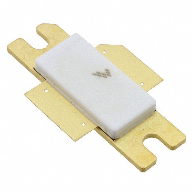
ICGOO电子元器件商城为您提供MRFE6S9045NR1由Freescale Semiconductor设计生产,在icgoo商城现货销售,并且可以通过原厂、代理商等渠道进行代购。 MRFE6S9045NR1价格参考。Freescale SemiconductorMRFE6S9045NR1封装/规格:晶体管 - FET,MOSFET - 射频, 射频 Mosfet LDMOS 28V 350mA 880MHz 22.1dB 10W TO-270-2。您可以下载MRFE6S9045NR1参考资料、Datasheet数据手册功能说明书,资料中有MRFE6S9045NR1 详细功能的应用电路图电压和使用方法及教程。
NXP USA Inc. 的 MRFE6S9045NR1 是一款高性能的射频功率 MOSFET 晶体管,属于 LDMOS(横向双扩散金属氧化物半导体)技术器件,广泛应用于高频率、高功率的射频放大场景。该器件特别适用于 806 MHz 至 960 MHz 频段,在工业、科学和医疗(ISM)频段以及陆地移动无线电(如公共安全通信、消防、警察电台)系统中表现优异。

MRFE6S9045NR1 常用于基站射频功率放大器模块,支持高效线性放大,适合需要高输出功率和良好热稳定性的应用。其典型应用场景包括蜂窝通信基础设施(如4G LTE基站)、高功率发射机、广播设备和大功率无线中继系统。该器件具备出色的耐用性和抗负载失配能力,可在复杂电磁环境中稳定工作,提升系统可靠性。

此外,由于其采用坚固的氮化铝基板封装,具有优良的散热性能,适合长时间高负荷运行,广泛用于需要高可用性和连续工作的关键通信系统。在现代无线通信网络升级和专用无线网络建设中,MRFE6S9045NR1 是实现高效、可靠射频放大的核心元件之一。
| 参数 | 数值 |
| 产品目录 | |
| 描述 | MOSFET RF N-CH 10W TO-270-2射频MOSFET晶体管 HV6E 45W NI270-2 FET |
| 产品分类 | RF FET分离式半导体 |
| 品牌 | Freescale Semiconductor |
| 产品手册 | |
| 产品图片 |
|
| rohs | 符合RoHS含铅 / 符合限制有害物质指令(RoHS)规范要求 |
| 产品系列 | 晶体管,晶体管射频,射频MOSFET晶体管,Freescale Semiconductor MRFE6S9045NR1- |
| 数据手册 | |
| 产品型号 | MRFE6S9045NR1 |
| Vds-Drain-SourceBreakdownVoltage | 66 V |
| Vds-漏源极击穿电压 | 66 V |
| Vgs-Gate-SourceBreakdownVoltage | - 0.5 V, 12 V |
| Vgs-栅源极击穿电压 | - 0.5 V, 12 V |
| 产品目录页面 | |
| 产品种类 | 射频MOSFET晶体管 |
| 供应商器件封装 | TO-270-2 |
| 其它名称 | MRFE6S9045NR1CT |
| 功率-输出 | 10W |
| 包装 | 剪切带 (CT) |
| 单位重量 | 529.550 mg |
| 商标 | Freescale Semiconductor |
| 噪声系数 | - |
| 增益 | 22.1dB |
| 安装风格 | SMD/SMT |
| 封装 | Reel |
| 封装/外壳 | TO-270AA |
| 封装/箱体 | TO-270 |
| 工厂包装数量 | 500 |
| 晶体管极性 | N-Channel |
| 晶体管类型 | LDMOS |
| 最大工作温度 | + 150 C |
| 最小工作温度 | - 65 C |
| 标准包装 | 1 |
| 汲极/源极击穿电压 | 66 V |
| 电压-测试 | 28V |
| 电压-额定 | 66V |
| 电流-测试 | 350mA |
| 系列 | MRFE6S9045NR1 |
| 配置 | Single |
| 闸/源击穿电压 | - 0.5 V, 12 V |
| 频率 | 880MHz |
| 额定电流 | 10µA |


- 商务部:美国ITC正式对集成电路等产品启动337调查
- 曝三星4nm工艺存在良率问题 高通将骁龙8 Gen1或转产台积电
- 太阳诱电将投资9.5亿元在常州建新厂生产MLCC 预计2023年完工
- 英特尔发布欧洲新工厂建设计划 深化IDM 2.0 战略
- 台积电先进制程称霸业界 有大客户加持明年业绩稳了
- 达到5530亿美元!SIA预计今年全球半导体销售额将创下新高
- 英特尔拟将自动驾驶子公司Mobileye上市 估值或超500亿美元
- 三星加码芯片和SET,合并消费电子和移动部门,撤换高东真等 CEO
- 三星电子宣布重大人事变动 还合并消费电子和移动部门
- 海关总署:前11个月进口集成电路产品价值2.52万亿元 增长14.8%


PDF Datasheet 数据手册内容提取
Freescale Semiconductor Document Number: MRFE6S9045N Technical Data Rev. 0, 10/2007 RF Power Field Effect Transistor N-Channel Enhancement-Mode Lateral MOSFET MRFE6S9045NR1 Designed for broadband commercial and industrial applications with fre- quencies up to 1000 MHz. The high gain and broadband performance of this device makes it ideal for large-signal, common-source amplifier applications in 28 volt base station equipment. • Typical Single-Carrier N-CDMA Performance @ 880 MHz, V = 28 Volts, DD I = 350 mA, P = 10 Watts Avg., IS-95 CDMA (Pilot, Sync, Paging, 880 MHz, 10 W AVG., 28 V DQ out Traffic Codes 8 Through 13) Channel Bandwidth = 1.2288 MHz. PAR = SINGLE N-CDMA 9.8 dB @ 0.01% Probability on CCDF. LATERAL N-CHANNEL Power Gain (cid:151) 22.1 dB BROADBAND Drain Efficiency (cid:151) 32% RF POWER MOSFET ACPR @ 750 kHz Offset (cid:151) -46 dBc in 30 kHz Channel Bandwidth • Capable of Handling 5:1 VSWR, @ 32 Vdc, 880 MHz, 3 dB Overdrive, Designed for Enhanced Ruggedness GSM EDGE Application • Typical GSM EDGE Performance: V = 28 Volts, I = 350 mA, DD DQ P = 16 Watts Avg., Full Frequency Band (920-960 MHz) out Power Gain (cid:151) 20 dB Drain Efficiency (cid:151) 46% CASE 1265-09, STYLE 1 Spectral Regrowth @ 400 kHz Offset = -62 dBc TO-270-2 Spectral Regrowth @ 600 kHz Offset = -78 dBc PLASTIC EVM (cid:151) 1.5% rms GSM Application • Typical GSM Performance: V = 28 Volts, I = 350 mA, P = 45 Watts, DD DQ out Full Frequency Band (920-960 MHz) Power Gain (cid:151) 20 dB Drain Efficiency (cid:151) 68% Features • Characterized with Series Equivalent Large-Signal Impedance Parameters • Integrated ESD Protection • 225°C Capable Plastic Package • RoHS Compliant • In Tape and Reel. R1 Suffix = 500 Units per 24 mm, 13 inch Reel. Table 1. Maximum Ratings Rating Symbol Value Unit Drain-Source Voltage VDSS -0.5, +66 Vdc Gate-Source Voltage VGS -0.5, +12 Vdc Maximum Operation Voltage VDD 32, +0 Vdc Storage Temperature Range Tstg -65 to +150 °C Case Operating Temperature TC 150 °C Operating Junction Temperature (1,2) TJ 225 °C Table 2. Thermal Characteristics Characteristic Symbol Value (2,3) Unit Thermal Resistance, Junction to Case RθJC °C/W Case Temperature 81°C, 45 W CW 1.0 Case Temperature 79°C, 10 W CW 1.1 1. Continuous use at maximum temperature will affect MTTF. 2. MTTF calculator available at http://www.freescale.com/rf. Select Tools (Software & Tools)/Calculators to access MTTF calculators by product. 3. Refer to AN1955, Thermal Measurement Methodology of RF Power Amplifiers. Go to http://www.freescale.com/rf. Select Documentation/Application Notes - AN1955. © Freescale Semiconductor, Inc., 2007. All rights reserved. MRFE6S9045NR1 RF Device Data Freescale Semiconductor 1
Table 3. ESD Protection Characteristics Test Methodology Class Human Body Model (per JESD22-A114) 3A (Minimum) Machine Model (per EIA/JESD22-A115) A (Minimum) Charge Device Model (per JESD22-C101) IV (Minimum) Table 4. Moisture Sensitivity Level Test Methodology Rating Package Peak Temperature Unit Per JESD 22-A113, IPC/JEDEC J-STD-020 3 260 °C Table 5. Electrical Characteristics (TC = 25°C unless otherwise noted) Characteristic Symbol Min Typ Max Unit Off Characteristics Zero Gate Voltage Drain Leakage Current IDSS (cid:151) (cid:151) 10 μAdc (VDS = 66 Vdc, VGS = 0 Vdc) Zero Gate Voltage Drain Leakage Current IDSS (cid:151) (cid:151) 1 μAdc (VDS = 28 Vdc, VGS = 0 Vdc) Gate-Source Leakage Current IGSS (cid:151) (cid:151) 10 μAdc (VGS = 5 Vdc, VDS = 0 Vdc) On Characteristics Gate Threshold Voltage VGS(th) 1 2 3 Vdc (VDS = 10 Vdc, ID = 200 μA) Gate Quiescent Voltage VGS(Q) 2.3 3.1 3.8 Vdc (VDD = 28 Vdc, ID = 350 mAdc, Measured in Functional Test) Drain-Source On-Voltage VDS(on) 0.05 0.23 0.3 Vdc (VGS = 10 Vdc, ID = 1.0 Adc) Dynamic Characteristics Reverse Transfer Capacitance Crss (cid:151) 1.02 (cid:151) pF (VDS = 28 Vdc ± 30 mV(rms)ac @ 1 MHz, VGS = 0 Vdc) Output Capacitance Coss (cid:151) 27 (cid:151) pF (VDS = 28 Vdc ± 30 mV(rms)ac @ 1 MHz, VGS = 0 Vdc) Input Capacitance Ciss (cid:151) 81 (cid:151) pF (VDS = 28 Vdc, VGS = 0 Vdc ± 30 mV(rms)ac @ 1 MHz) Functional Tests (In Freescale Test Fixture, 50 ohm system) VDD = 28 Vdc, IDQ = 350 mA, Pout = 10 W Avg., f = 880 MHz, Single-Carrier N-CDMA, 1.2288 MHz Channel Bandwidth Carrier. ACPR measured in 30 kHz Channel Bandwidth @ ±750 kHz Offset. PAR = 9.8 dB @ 0.01% Probability on CCDF Power Gain Gps 21 22.1 25 dB Drain Efficiency ηD 30.5 32 (cid:151) % Adjacent Channel Power Ratio ACPR (cid:151) -46 -44 dBc Input Return Loss IRL (cid:151) -19 -9 dB (continued) MRFE6S9045NR1 RF Device Data 2 Freescale Semiconductor
Table 5. Electrical Characteristics (TC = 25°C unless otherwise noted) (continued) Characteristic Symbol Min Typ Max Unit Typical GSM EDGE Performances (In Freescale GSM EDGE Test Fixture Optimized for 920-960 MHz, 50 ohm system) VDD = 28 Vdc, IDQ = 350 mA, Pout = 16 W Avg., f = 920-960 MHz, GSM EDGE Signal Power Gain Gps (cid:151) 20 (cid:151) dB Drain Efficiency ηD (cid:151) 46 (cid:151) % Error Vector Magnitude EVM (cid:151) 1.5 (cid:151) % Spectral Regrowth at 400 kHz Offset SR1 (cid:151) -62 (cid:151) dBc Spectral Regrowth at 600 kHz Offset SR2 (cid:151) -78 (cid:151) dBc Typical CW Performances (In Freescale GSM Test Fixture Optimized for 920-960 MHz, 50 ohm system) VDD = 28 Vdc, IDQ = 350 mA, Pout = 45 W, f = 920-960 MHz Power Gain Gps (cid:151) 20 (cid:151) dB Drain Efficiency ηD (cid:151) 68 (cid:151) % Input Return Loss IRL (cid:151) -12 (cid:151) dB Pout @ 1 dB Compression Point P1dB (cid:151) 52 (cid:151) W (f = 940 MHz) Typical Performances (In Freescale Test Fixture, 50 ohm system) VDD = 28 Vdc, IDQ = 350 mA, 865-900 MHz Bandwidth Video Bandwidth @ 48 W PEP Pout where IM3 = -30 dBc VBW MHz (Tone Spacing from 100 kHz to VBW) (cid:151) 10 (cid:151) ΔIMD3 = IMD3 @ VBW frequency - IMD3 @ 100 kHz <1 dBc (both sidebands) Gain Flatness in 35 MHz Bandwidth @ Pout = 10 W Avg. GF (cid:151) 0.72 (cid:151) dB Gain Variation over Temperature ΔG (cid:151) 0.011 (cid:151) dB/°C (-30°C to +85°C) Output Power Variation over Temperature ΔP1dB (cid:151) 0.006 (cid:151) dBm/°C (-30°C to +85°C) MRFE6S9045NR1 RF Device Data Freescale Semiconductor 3
B2 B1 VSUPPLY + + + R1 VBIAS L2 C10 C16 C17 C18 + R3 R2 C15 C7 L1 C8 RF RF Z10 Z11 Z12 Z13 Z14 Z15 Z16 OUTPUT C5 INPUT Z1 Z2 Z3 Z4 Z5 Z6 Z7 Z8 Z9 C14 C9 C11 C12 C13 C1 DUT C2 C3 C4 C6 Z1 0.215″ x 0.065″ Microstrip Z10 0.360″ x 0.270″ Microstrip Z2 0.221″ x 0.065″ Microstrip Z11 0.063″ x 0.270″ Microstrip Z3 0.500″ x 0.100″ Microstrip Z12 0.360″ x 0.065″ Microstrip Z4 0.460″ x 0.270″ Microstrip Z13 0.095″ x 0.065″ Microstrip Z5 0.040″ x 0.270″ Microstrip Z14 0.800″ x 0.065″ Microstrip Z6 0.280″ x 0.270″ x 0.530″Taper Z15 0.260″ x 0.065″ Microstrip Z7 0.087″ x 0.525″ Microstrip Z16 0.325″ x 0.065″ Microstrip Z8 0.435″ x 0.525″ Microstrip PCB Taconic RF-35 0.030″, εr = 3.5 Z9 0.057″ x 0.525″ Microstrip Figure 1. MRFE6S9045NR1 Test Circuit Schematic Table 6. MRFE6S9045NR1 Test Circuit Component Designations and Values Part Description Part Number Manufacturer B1 Ferrite Bead 2743019447 Fair Rite B2 Ferrite Bead 2743021447 Fair Rite C1, C7, C10, C14 47 pF Chip Capacitors ATC100B470JT500XT ATC C2, C4, C12 0.8-8.0 pF Variable Capacitors, Gigatrim 27291SL Johanson C3 15 pF Chip Capacitor ATC100B150JT500XT ATC C5, C6 12 pF Chip Capacitors ATC100B120JT500XT ATC C8, C9 13 pF Chip Capacitors ATC100B130JT500XT ATC C11 7.5 pF Chip Capacitor ATC100B7R5JT500XT ATC C13 0.6-4.5 pF Variable Capacitor, Gigatrim 27271SL Johanson C15, C16, C17 10 μF, 35 V Tantalum Capacitors T491D106K035AT Kemet C18 220 μF, 50 V Electrolytic Capacitor EMVY500ADA221MJA0G Nippon Chemi-con L1, L2 12.5 nH Inductors A04T-5 Coilcraft R1 1 kΩ, 1/4 W Chip Resistor CRCW12061001FKEA Vishay R2 560 kΩ, 1/4 W Chip Resistor CRCW120656001FKEA Vishay R3 12 Ω, 1/4 W Chip Resistor CRCW120612R0FKEA Vishay MRFE6S9045NR1 RF Device Data 4 Freescale Semiconductor
C15 R2 C18 R3 VDD R1 B1 VGG C16C17 B2 C7 C10 L2 L1 C5 C8 C1 C2 C4 C14 A C3 C6 RE A C11 C13 T C9 U C12 O T U C TO−270/272 Surface / Bolt down Figure 2. MRFE6S9045NR1 Test Circuit Component Layout MRFE6S9045NR1 RF Device Data Freescale Semiconductor 5
TYPICAL CHARACTERISTICS 23 34 %) 22 ηD Gps 32 DRAINENCY ( 21 30 , DCI WER GAIN (dB) 2109 VPNTrDo−auDCftf iD==c M12C08Ao dWVISed s−(cA 98v5 gT P.h)i rlIooDutQ gS h=y n13c35, 0P magAing IRL −−3400 ηdBc)EFFI 0−5 OSS (dB) G, POps1187 ACPR −−5600 R (dBc), ALT1 ( −−1150 UT RETURN L ALT1 CP NP 16 −70 A −20 L, I 800 820 840 860 880 900 920 940 960 R I f, FREQUENCY (MHz) Figure 3. Single-Carrier N-CDMA Broadband Performance @ P = 10 Watts Avg. out 23 50 ηD %) 22 40 AINCY ( RN 21 Gps 30 , DDCIE B) η FI N (d 20 VDD = 28 Vdc, Pout = 20 W (Avg.) −20 EF AI IDQ = 350 mA, N−CDMA IS−95 Pilot B) G, POWER Gps 11119876 ALTST1hynrocu, gPha g1i3ng, Traffic Codes 8 ACPR −−−−34560000 R (dBc), ALT1 (dBc) −0−150 UT RETURN LOSS (d 15800 820 840 860 IRL880 900 920 940 960−70 ACP −15 RL, INP I f, FREQUENCY (MHz) Figure 4. Single-Carrier N-CDMA Broadband Performance @ P = 20 Watts Avg. out 24 −10 IDQ = 525 mA 437.5 mA c) VDD = 28 Vdc, f1 = 880 MHz, f2 = 880.1 MHz 23 B Two−Tone Measurements d N ( −20 ER GAIN (dB) 2221 32561027 .5m5 mAmAA RD ORDERN DISTORTIO −30 IDQ = 175 mA OW 20 THITIO −40 262.5 mA G, Pps 19 IMD, ODULA 350 mA M R −50 18 VDD = 28 Vdc, f1 = 880 MHz, f2 = 880.1 MHz TE 437.5 mA 525 mA Two−Tone Measurements N I 17 −60 1 10 100 200 1 10 100 200 Pout, OUTPUT POWER (WATTS) PEP Pout, OUTPUT POWER (WATTS) PEP Figure 5. Two-Tone Power Gain versus Figure 6. Third Order Intermodulation Distortion Output Power versus Output Power MRFE6S9045NR1 RF Device Data 6 Freescale Semiconductor
TYPICAL CHARACTERISTICS −10 0 N (dBc) −20 Vf2D =D 8=8 208.1 V MdcH,z I,D TQw =o −3T5o0n me AM, ef1a s=u 8re8m0 eMnHtsz N (dBc) −10 VTwDDo− =T o2n8e V Mdce,a Psouurte =m 4e8n tWs (PEP), IDQ = 350 mA O O (f1 + f2)/2 = Center Frequency of 880 MHz TI TI R −30 R −20 O O T T IM3−L S S IM3−U DI −40 DI −30 N N ATIO −50 3rd Order ATIO −40 DUL DUL IM5−L IM7−L IM7−U MO −60 5th Order MO −50 IM5−U R R E E NT −70 NT −60 D, I 7th Order D, I M M I −80 I −70 1 10 100 200 1 10 100 Pout, OUTPUT POWER (WATTS) PEP TWO−TONE SPACING (MHz) Figure 7. Intermodulation Distortion Products Figure 8. Intermodulation Distortion Products versus Output Power versus Tone Spacing 56 Ideal 55 P6dB = 49.21 dBm (83.36 W) 54 m) dB 53 P3dB = 48.40 dBm (69.18 W) R ( E 52 W O P 51 T P1dB = 47.38 dBm U TP 50 (54.7 W) U O 49 P, out 48 Actual 47 VDD = 28 Vdc, IDQ = 350 mA, Pulsed CW 12 μsec(on), 1% Duty Cycle, f = 880 MHz 46 24 25 26 27 28 29 30 31 32 33 34 Pin, INPUT POWER (dBm) Figure 9. Pulsed CW Output Power versus Input Power WER GAIN (dB) 7566500505 VfST =hyD nrD8oc 8u=, 0g P2 hMa8 g 1HVi3nzdg,c ,N, TI−DrCaQfD f=icM 3CA5o 0IdS me−sA9 58 Pilot −30(cid:2)C85(cid:2)22C55(cid:2)(cid:2)CC −−−−−522115050 R RATIO (dBc)dBc) Y (%), G, POps 43430055 ACPR 88552(cid:2)(cid:2)5CC(cid:2)C −−3300(cid:2)(cid:2)CC −−−−43345050 ANNEL POWENEL POWER ( N EFFICIENC 12210055 Gps ηD 85(cid:2)CTC25 =(cid:2) −C30(cid:2)C −−−−56565500 DJACENT CHALT1, CHAN η, DRAID 051 ALT1 10 100−−7705 ACPR, A Pout, OUTPUT POWER (WATTS) AVG. Figure 10. Single-Carrier N-CDMA ACPR, ALT1, Power Gain and Drain Efficiency versus Output Power MRFE6S9045NR1 RF Device Data Freescale Semiconductor 7
TYPICAL CHARACTERISTICS 23 80 23 TC = −30(cid:2)C 25(cid:2)C −30(cid:2)C IDQ = 350 mA 22 25(cid:2)C 70 f = 880 MHz 85(cid:2)C 22 dB) 21 Gps 60 %) GAIN ( 20 85(cid:2)C 50 NCY ( N (dB) 21 ER CIE GAI W 19 40 FI R , POps 18 30 AIN EF POWE 20 G DR , ps 17 ηD VDD = 28 Vdc 20 η, D G 19 16 IfD =Q 8 =8 03 5M0H mzA 10 VDD = 24 V 28 V 32 V 15 0 18 1 10 100 0 20 40 60 80 100 Pout, OUTPUT POWER (WATTS) CW Pout, OUTPUT POWER (WATTS) CW Figure 11. Power Gain and Drain Efficiency Figure 12. Power Gain versus Output Power versus CW Output Power 108 107 S) R U O H F ( T T M 106 105 90 110 130 150 170 190 210 230 250 TJ, JUNCTION TEMPERATURE (°C) This above graph displays calculated MTTF in hours when the device is operated at VDD = 28 Vdc, Pout = 10 W Avg., and ηD = 32%. MTTF calculator available at http:/www.freescale.com/rf. Select Tools (Software & Tools)/Calculators to access MTTF calculators by product. Figure 13. MTTF versus Junction Temperature MRFE6S9045NR1 RF Device Data 8 Freescale Semiconductor
N-CDMA TEST SIGNAL 100 −10 1.2288 MHz −20 Channel BW PROBABILITY (%) 0.00.0001.11011 ITC±B0S.ha7a0−rn5r1o9rd0i%u5ew g kr CisPHhd.D rt z1hAo M3O bC@)Aaf Pf1b s (R±.iePl2i 1tti2M.yl. o89 Aeot88,Lan TSsM MC1uyH nrCHMezcDzd ,e C FPOain.hsaf afu3gsnr0ieenn tdgk.e ,HPli nTBAz r a3RaBn0f af=d inkc wH9 dCi.wdz8o ti hddd teBhs @ @8 (dB) −−−−−−−63457890000000 ............................................................................................−.................I......A...n....................L..t..........e........T...............g.......1.............r........ ......a......i..........n......t..........e.... ...........3....d.......−..........0...... .......A....I..B.. ........n....k......C......W......t..H........e........P............z..g..........R...........r............a...... ...........i......t..n........e.............. ......d....3................... ....0.......B.............. ..........k..W.................H...........................z.....................................................................................+.......................A......I........n...........C.........t............e......P................g............R.........r............a.... ...........i.....t...n.......e............. ........d...3................. ..0........+..B............ ....I....A...k...Wn...............H....L..t.........e........T.....z.........g........1...........r........ ......a......i........n......t.........e...... ...........3....d..................0...... .............B.. ............k............W........H............................z............................................................................. 0.0001 0 2 4 6 8 10 −100 PEAK−TO−AVERAGE (dB) −110 Figure 14. Single-Carrier CCDF N-CDMA −3.6 −2.9 −2.2 −1.5 −0.7 0 0.7 1.5 2.2 2.9 3.6 f, FREQUENCY (MHz) Figure 15. Single-Carrier N-CDMA Spectrum MRFE6S9045NR1 RF Device Data Freescale Semiconductor 9
Zo = 5 Ω f = 910 MHz f = 850 MHz Zsource Zload f = 910 MHz f = 850 MHz VDD = 28 Vdc, IDQ = 350 mA, Pout = 10 W Avg. f Zsource Zload MHz Ω Ω 850 0.42 + j0.30 3.05 + j1.27 865 0.42 + j0.44 3.16 + j1.33 880 0.45 + j0.60 3.31 + j1.33 895 0.48 + j0.74 3.43 + j1.20 910 0.50 + j0.85 3.35 + j1.05 Zsource = Test circuit impedance as measured from gate to ground. Zload = Test circuit impedance as measured from drain to ground. Input Device Output Matching Under Matching Network Test Network Z Z source load Figure 16. Series Equivalent Source and Load Impedance MRFE6S9045NR1 RF Device Data 10 Freescale Semiconductor
PACKAGE DIMENSIONS MRFE6S9045NR1 RF Device Data Freescale Semiconductor 11
MRFE6S9045NR1 RF Device Data 12 Freescale Semiconductor
MRFE6S9045NR1 RF Device Data Freescale Semiconductor 13
PRODUCT DOCUMENTATION Refer to the following documents to aid your design process. Application Notes • AN1907: Solder Reflow Attach Method for High Power RF Devices in Plastic Packages • AN1955: Thermal Measurement Methodology of RF Power Amplifiers • AN3263: Bolt Down Mounting Method for High Power RF Transistors and RFICs in Over-Molded Plastic Packages Engineering Bulletins • EB212: Using Data Sheet Impedances for RF LDMOS Devices REVISION HISTORY The following table summarizes revisions to this document. Revision Date Description 0 Oct. 2007 • Initial Release of Data Sheet MRFE6S9045NR1 RF Device Data 14 Freescale Semiconductor
How to Reach Us: Home Page: www.freescale.com Web Support: http://www.freescale.com/support USA/Europe or Locations Not Listed: Freescale Semiconductor, Inc. Technical Information Center, EL516 2100 East Elliot Road Tempe, Arizona 85284 +1-800-521-6274 or +1-480-768-2130 www.freescale.com/support Europe, Middle East, and Africa: Freescale Halbleiter Deutschland GmbH Technical Information Center Information in this document is provided solely to enable system and software Schatzbogen 7 implementers to use Freescale Semiconductor products. There are no express or 81829 Muenchen, Germany implied copyright licenses granted hereunder to design or fabricate any integrated +44 1296 380 456 (English) +46 8 52200080 (English) circuits or integrated circuits based on the information in this document. +49 89 92103 559 (German) +33 1 69 35 48 48 (French) Freescale Semiconductor reserves the right to make changes without further notice to www.freescale.com/support any products herein. Freescale Semiconductor makes no warranty, representation or guarantee regarding the suitability of its products for any particular purpose, nor does Japan: Freescale Semiconductor assume any liability arising out of the application or use of Freescale Semiconductor Japan Ltd. any product or circuit, and specifically disclaims any and all liability, including without Headquarters limitation consequential or incidental damages. (cid:147)Typical(cid:148) parameters that may be ARCO Tower 15F 1-8-1, Shimo-Meguro, Meguro-ku, provided in Freescale Semiconductor data sheets and/or specifications can and do Tokyo 153-0064 vary in different applications and actual performance may vary over time. All operating Japan parameters, including (cid:147)Typicals(cid:148), must be validated for each customer application by 0120 191014 or +81 3 5437 9125 customer(cid:146)s technical experts. Freescale Semiconductor does not convey any license support.japan@freescale.com under its patent rights nor the rights of others. Freescale Semiconductor products are not designed, intended, or authorized for use as components in systems intended for Asia/Pacific: surgical implant into the body, or other applications intended to support or sustain life, Freescale Semiconductor Hong Kong Ltd. or for any other application in which the failure of the Freescale Semiconductor product Technical Information Center could create a situation where personal injury or death may occur. Should Buyer 2 Dai King Street Tai Po Industrial Estate purchase or use Freescale Semiconductor products for any such unintended or Tai Po, N.T., Hong Kong unauthorized application, Buyer shall indemnify and hold Freescale Semiconductor +800 2666 8080 and its officers, employees, subsidiaries, affiliates, and distributors harmless against all support.asia@freescale.com claims, costs, damages, and expenses, and reasonable attorney fees arising out of, directly or indirectly, any claim of personal injury or death associated with such For Literature Requests Only: unintended or unauthorized use, even if such claim alleges that Freescale Freescale Semiconductor Literature Distribution Center Semiconductor was negligent regarding the design or manufacture of the part. P.O. Box 5405 Denver, Colorado 80217 1-800-441-2447 or 303-675-2140 Freescale(cid:3) and the Freescale logo are trademarks of Freescale Semiconductor, Inc. Fax: 303-675-2150 All other product or service names are the property of their respective owners. LDCForFreescaleSemiconductor@hibbertgroup.com © Freescale Semiconductor, Inc. 2007. All rights reserved. MRFE6S9045NR1 RDFo cDuemveinct eN uDmabtear: MRFE6S9045N FRreeve. s0c, 1a0le/2 0S07emiconductor 15
Mouser Electronics Authorized Distributor Click to View Pricing, Inventory, Delivery & Lifecycle Information: N XP: MRFE6S9045NR1