ICGOO在线商城 > 分立半导体产品 > 晶体管 - FET,MOSFET - 射频 > MRF6V3090NBR5
 Datasheet下载
- 型号: MRF6V3090NBR5
- 制造商: Freescale Semiconductor
- 库位|库存: xxxx|xxxx
- 要求:
| 数量阶梯 | 香港交货 | 国内含税 |
| +xxxx | $xxxx | ¥xxxx |
查看当月历史价格
查看今年历史价格
MRF6V3090NBR5产品简介:
ICGOO电子元器件商城为您提供MRF6V3090NBR5由Freescale Semiconductor设计生产,在icgoo商城现货销售,并且可以通过原厂、代理商等渠道进行代购。 MRF6V3090NBR5价格参考。Freescale SemiconductorMRF6V3090NBR5封装/规格:晶体管 - FET,MOSFET - 射频, RF Mosfet LDMOS 50V 350mA 860MHz 22dB 18W TO-272 WB-4。您可以下载MRF6V3090NBR5参考资料、Datasheet数据手册功能说明书,资料中有MRF6V3090NBR5 详细功能的应用电路图电压和使用方法及教程。
NXP USA Inc. 的 MRF6V3090NBR5 是一款高功率射频MOSFET晶体管,属于N系列LDMOS(横向双扩散金属氧化物半导体)器件,广泛应用于射频功率放大场景。该器件工作频率可达1.2 GHz以下,输出功率高达90W,具有高增益、高效率和良好的热稳定性,适用于需要高可靠性和持续功率输出的系统。

其主要应用场景包括:

1. 无线通信基站:用于蜂窝网络基础设施中的射频功率放大,支持GSM、CDMA、WCDMA等多种移动通信标准,尤其适用于宏蜂窝基站的最终级放大。

2. 工业、科学和医疗(ISM)频段设备:在400–900 MHz频段内,用于射频能量应用,如加热、等离子生成和医疗射频治疗设备。

3. 公共安全与陆地移动无线电(LMR):适用于警察、消防、急救等系统的专用无线通信设备,提供稳定可靠的语音和数据传输。

4. 广播与航空通信:可用于FM广播发射机或航空地空通信系统中的射频放大模块。

MRF6V3090NBR5采用坚固的陶瓷封装(SOT-789A),具备出色的散热性能和抗负载失配能力,适合在严苛环境下长期运行。配合适当的匹配电路和散热设计,可在高驻波比(VSWR)条件下保持稳定工作,是高性能射频功率放大的理想选择。
| 参数 | 数值 |
| 产品目录 | |
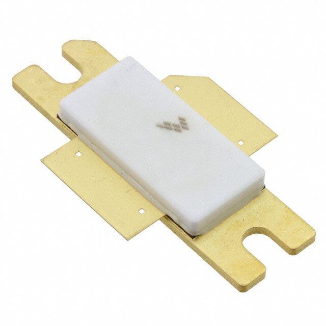
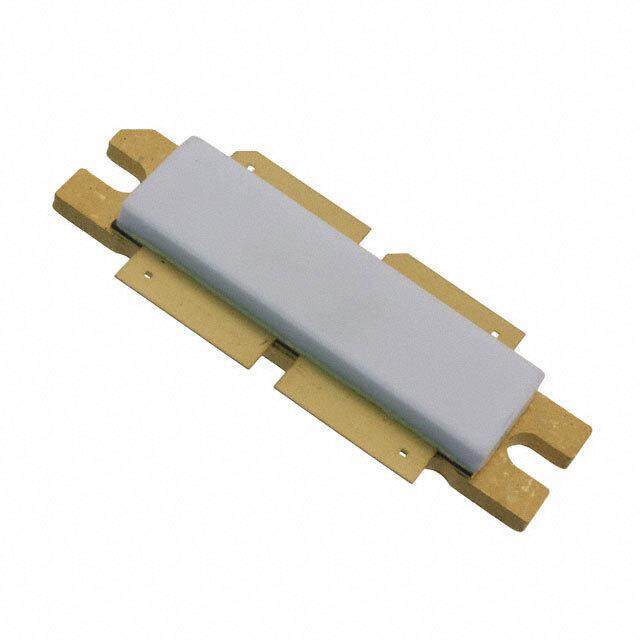
| 描述 | FET RF N-CH 860MHZ 50V TO272-4射频MOSFET晶体管 VHV6 860MHz 90W TO 272WB4 |
| 产品分类 | RF FET分离式半导体 |
| 品牌 | Freescale Semiconductor |
| 产品手册 | |
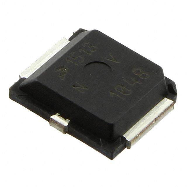
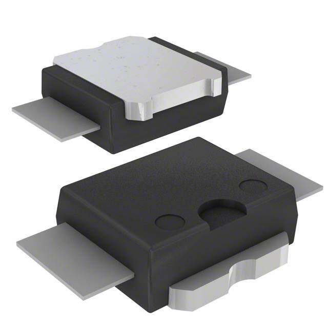
| 产品图片 |
|
| rohs | 符合RoHS不受无铅要求限制 / 符合限制有害物质指令(RoHS)规范要求 |
| 产品系列 | 晶体管,晶体管射频,射频MOSFET晶体管,Freescale Semiconductor MRF6V3090NBR5- |
| 数据手册 | |
| 产品型号 | MRF6V3090NBR5 |
| Vds-Drain-SourceBreakdownVoltage | 115 V |
| Vds-漏源极击穿电压 | 115 V |
| Vgs-Gate-SourceBreakdownVoltage | 10 V |
| Vgs-栅源极击穿电压 | 10 V |
| Vgsth-Gate-SourceThresholdVoltage | 2.4 V |
| Vgsth-栅源极阈值电压 | 2.4 V |
| 产品种类 | 射频MOSFET晶体管 |
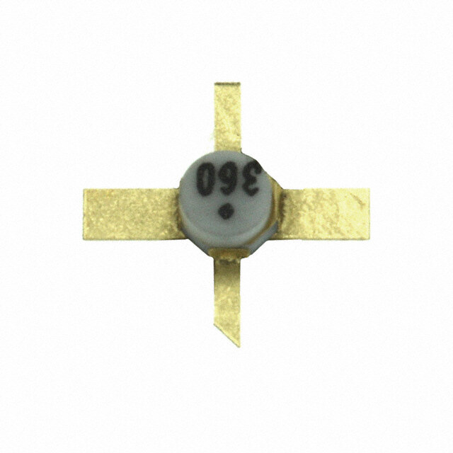
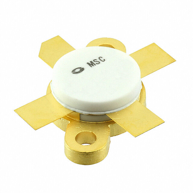
| 供应商器件封装 | TO-272 WB-4 |
| 其它名称 | MRF6V3090NBR5CT |
| 功率-输出 | 18W |
| 包装 | 剪切带 (CT) |
| 单位重量 | 2 g |
| 商标 | Freescale Semiconductor |
| 噪声系数 | - |
| 增益 | 22dB |
| 安装风格 | SMD/SMT |
| 封装 | Reel |
| 封装/外壳 | TO-272BB |
| 封装/箱体 | TO-270-4 WB |
| 工厂包装数量 | 50 |
| 晶体管极性 | N-Channel |
| 晶体管类型 | LDMOS |
| 最大工作温度 | + 150 C |
| 标准包装 | 1 |
| 汲极/源极击穿电压 | 115 V |
| 电压-测试 | 50V |
| 电压-额定 | 110V |
| 电流-测试 | 350mA |
| 系列 | MRF6V3090N |
| 输出功率 | 18 W |
| 配置 | Single |
| 闸/源击穿电压 | 10 V |
| 频率 | 860MHz |
| 额定电流 | - |


- 商务部:美国ITC正式对集成电路等产品启动337调查
- 曝三星4nm工艺存在良率问题 高通将骁龙8 Gen1或转产台积电
- 太阳诱电将投资9.5亿元在常州建新厂生产MLCC 预计2023年完工
- 英特尔发布欧洲新工厂建设计划 深化IDM 2.0 战略
- 台积电先进制程称霸业界 有大客户加持明年业绩稳了
- 达到5530亿美元!SIA预计今年全球半导体销售额将创下新高
- 英特尔拟将自动驾驶子公司Mobileye上市 估值或超500亿美元
- 三星加码芯片和SET,合并消费电子和移动部门,撤换高东真等 CEO
- 三星电子宣布重大人事变动 还合并消费电子和移动部门
- 海关总署:前11个月进口集成电路产品价值2.52万亿元 增长14.8%

PDF Datasheet 数据手册内容提取
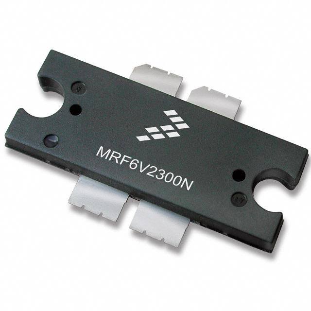
Freescale Semiconductor DocumentNumber:MRF6V3090N Technical Data Rev.2,10/2015 RF Power LDMOS Transistors N--Channel Enhancement--Mode Lateral MOSFETs MRF6V3090N Designedforbroadcastandcommercialaerospacebroadbandapplications MRF6V3090NB withfrequenciesfrom470to1215MHz. TypicalPerformance(UHF470--860ReferenceCircuit):VDD=50Volts, I =450mA,64QAM,InputSignalPAR=9.5dB@0.01%Probability DQ onCCDF. Output IMD 470--1215MHz,90W,50V Pout f Gps D SignalPAR Shoulder BROADBAND SignalType (W) (MHz) (dB) (%) (dB) (dBc) RFPOWERLDMOSTRANSISTORS DVB--T(8kOFDM) 18Avg. 470 21.6 26.8 8.6 --31.8 650 22.9 28.0 8.7 --34.4 860 21.9 28.3 7.9 --29.2 TO--270WB--4 TypicalPerformance(L--Band960--1215MHzReferenceCircuit): PLASTIC V =50Volts,I =100mA. DD DQ MRF6V3090N Pout f Pin Gps D SignalType (W) (MHz) (W) (dB) (%) Pulse 90Peak 960 1.3 18.4 55.3 (128sec,10%Duty 1030 1.41 18 56.9 Cycle) 1090 1.65 17.4 50.7 TO--272WB--4 1215 1.68 17.3 51.0 PLASTIC MRF6V3090NB Features CapableofHandling10:1VSWR,AllPhaseAngles,@50Vdc,860MHz, PARTSARESINGLE--ENDED 90WattsCWOutputPower CharacterizedwithSeriesEquivalentLarge--SignalImpedanceParameters InternallyInputMatchedforEaseofUse QualifiedUptoaMaximumof50VDDOperation IntegratedESDProtection Gate Drain ExcellentThermalStability GreaterNegativeGate--SourceVoltageRangeforImprovedClassC Operation Gate Drain (TopView) Note: Exposedbacksideofthepackageis thesourceterminalforthetransistor. Figure1.PinConnections FreescaleSemiconductor,Inc.,2010--2011,2015.Allrightsreserved. MRF6V3090NMRF6V3090NB RFDeviceData FreescaleSemiconductor,Inc. 1
Table1.MaximumRatings Rating Symbol Value Unit Drain--SourceVoltage VDSS --0.5,+110 Vdc Gate--SourceVoltage VGS --6.0,+10 Vdc StorageTemperatureRange Tstg --65to+150 C CaseOperatingTemperature TC 150 C OperatingJunctionTemperature(1,2) TJ 225 C Table2.ThermalCharacteristics Characteristic Symbol Value(2,3) Unit ThermalResistance,JunctiontoCase RJC C/W CaseTemperature76C,18WCW,50Vdc,IDQ=350mA,860MHz 0.79 CaseTemperature80C,90WCW,50Vdc,IDQ=350mA,860MHz 0.82 Table3.ESDProtectionCharacteristics TestMethodology Class HumanBodyModel(perJESD22--A114) 2(2001--4000V) MachineModel(perEIA/JESD22--A115) B(201--400V) ChargeDeviceModel(perJESD22--C101) IV(>1000V) Table4.MoistureSensitivityLevel TestMethodology Rating PackagePeakTemperature Unit PerJESD22--A113,IPC/JEDECJ--STD--020 3 260 C Table5.ElectricalCharacteristics (TA=25Cunlessotherwisenoted) Characteristic Symbol Min Typ Max Unit OffCharacteristics Gate--SourceLeakageCurrent IGSS — — 0.5 Adc (VGS=5Vdc,VDS=0Vdc) Drain--SourceBreakdownVoltage V(BR)DSS 115 — — Vdc (ID=50mA,VGS=0Vdc) ZeroGateVoltageDrainLeakageCurrent IDSS — — 10 Adc (VDS=50Vdc,VGS=0Vdc) ZeroGateVoltageDrainLeakageCurrent IDSS — — 20 Adc (VDS=100Vdc,VGS=0Vdc) OnCharacteristics GateThresholdVoltage VGS(th) 0.9 1.6 2.4 Vdc (VDS=10Vdc,ID=200Adc) GateQuiescentVoltage VGS(Q) 2.0 2.7 3.5 Vdc (VDD=50Vdc,ID=350mAdc,MeasuredinFunctionalTest) Drain--SourceOn--Voltage VDS(on) — 0.2 — Vdc (VGS=10Vdc,ID=0.5Adc) DynamicCharacteristics ReverseTransferCapacitance Crss — 41 — pF (VDS=50Vdc30mV(rms)ac@1MHz,VGS=0Vdc) OutputCapacitance Coss — 65.4 — pF (VDS=50Vdc30mV(rms)ac@1MHz,VGS=0Vdc) InputCapacitance(4) Ciss — 591 — pF (VDS=50Vdc,VGS=0Vdc30mV(rms)ac@1MHz) 1. ContinuoususeatmaximumtemperaturewillaffectMTTF. 2. MTTFcalculatoravailableathttp://www.freescale.com/rf.SelectSoftware&Tools/DevelopmentTools/CalculatorstoaccessMTTF calculatorsbyproduct. 3. RefertoAN1955,ThermalMeasurementMethodologyofRFPowerAmplifiers.Gotohttp://www.freescale.com/rf. SelectDocumentation/ApplicationNotes--AN1955. 4. Partinternallyinputmatched. (continued) MRF6V3090NMRF6V3090NB RFDeviceData 2 FreescaleSemiconductor,Inc.
Table5.ElectricalCharacteristics (TA=25Cunlessotherwisenoted)(continued) Characteristic Symbol Min Typ Max Unit FunctionalTests(InFreescaleDVB--TNarrowbandTestFixture,50ohmsystem)VDD=50Vdc,IDQ=350mA,Pout=18WAvg., f=860MHz,DVB--T(8kOFDM)SingleChannel.ACPRmeasuredin7.61MHzChannelBandwidth@4MHzOffset@4kHzBandwidth. PowerGain Gps 21.0 22.0 24.0 dB DrainEfficiency D 27.5 28.5 — % AdjacentChannelPowerRatio ACPR — --62.0 --60.0 dBc InputReturnLoss IRL — --14 --9 dB Table6.OrderingInformation Device TapeandReelInformation Package MRF6V3090NR1 TO--270WB--4 R1Suffix=500Units,44mmTapeWidth,13--inchReel MRF6V3090NBR1 TO--272WB--4 MRF6V3090NR5 TO--270WB--4 R5Suffix=50Units,56mmTapeWidth,13--inchReel MRF6V3090NBR5 TO--272WB--4 MRF6V3090NMRF6V3090NB RFDeviceData FreescaleSemiconductor,Inc. 3
VSUPPLY + VBIAS C8 C9 C10 + R1 C1 C2 C3 Z8 Z10 RF C4 R2 OUTPUT RF Z9 Z12 Z13 Z14 Z15 Z16 Z17 Z18 INPUT Z1 Z2 Z3 Z4 Z5 Z6 Z7 C14 C5 C15 C11 C12 C13 DUT C6 C7 Z11 + C16 C17 C18 Z1 0.2660.067Microstrip Z10,Z11 1.2920.079Microstrip Z2 0.3310.067Microstrip Z12 0.6800.571Microstrip Z3 0.5980.067Microstrip Z13 0.1320.117Microstrip Z4 0.3150.276Microstrip Z14 0.7050.117Microstrip Z5 0.0540.669Microstrip Z15 0.1590.117Microstrip Z6 0.4190.669Microstrip Z16 0.1400.067Microstrip Z7 0.2560.669Microstrip Z17 0.0770.067Microstrip Z8 0.9860.071Microstrip Z18 0.1630.067Microstrip Z9 0.2010.571Microstrip Figure2.MRF6V3090N860MHzNarrowbandTestCircuitSchematic Table7.MRF6V3090N860MHzNarrowbandTestCircuitComponentDesignationsandValues Part Description PartNumber Manufacturer C1 22F,35VTantalumCapacitor T491X226K035AT Kermet C2,C9,C17 10F,50VChipCapacitors GRM55DR61H106KA88L Murata C3,C5,C8,C14,C16 43pFChipCapacitors ATC100B430JT500XT ATC C4 6.2pFChipCapacitor ATC100B6R2BT500XT ATC C6 2.2pFChipCapacitor ATC100B2R2JT500XT ATC C7 9.1pFChipCapacitor ATC100B9R1CT500XT ATC C10,C18 220F,100VElectrolyticCapacitors EEVFK2A221M Panasonic--ECG C11,C15 7.5pFChipCapacitors ATC100B7R5CT500XT ATC C12 3.0pFChipCapacitor ATC100B3R0CT500XT ATC C13 0.7pFChipCapacitor ATC100B0R7BT500XT ATC R1 10k,1/4WChipResistor CRCW120610KOJNEA Vishay R2 10,1/4WChipResistor CRCW120610ROJNEA Vishay PCB 0.030,r=3.5 RF--35 Taconic MRF6V3090NMRF6V3090NB RFDeviceData 4 FreescaleSemiconductor,Inc.
-- C1 C10 C8 C9 R1 C2 C3 C11 C14 C4 R2 A C15 E C5 C6 R C12 C13 A T U C7 O T U MRF6V3090N C Rev.0 C16 C17 C18 -- Figure3.MRF6V3090N860MHzNarrowbandTestCircuitComponentLayout MRF6V3090NMRF6V3090NB RFDeviceData FreescaleSemiconductor,Inc. 5
TYPICALCHARACTERISTICS 1000 24 70 Ciss VDD=50Vdc,IDQ=350mA,f=860MHz 23 60 Gps %) NCE(pF) GAIN(dB) 2212 5400 CIENCY( C,CAPACITA 100 CCorssss G,POWERps 1290 3200 DRAINEFFID, D 18 10 Measuredwith30mV(rms)ac@1MHz,VGS=0Vdc 10 17 0 0 10 20 30 40 50 1 10 100 200 VDS,DRAIN--SOURCEVOLTAGE(VOLTS) Pout,OUTPUTPOWER(WATTS) Figure4.CapacitanceversusDrain--SourceVoltage Figure5.CWPowerGainandDrainEfficiency versusOutputPower(NarrowbandTestCircuit) 56 25 P3dB=51.28dBm(134.3W) Ideal IDQ=350mA,f=860MHz 55 24 m) 54 P2dB=51.06dBm(127.6W) 23 OWER(dB 5532 P1dB=50.7dBm(117.5W) GAIN(dB) 2212 P Actual R UT 51 WE 20 P O P,OUTout 5409 G,Pps 1189 45V 50V 48 17 VDD=50Vdc,IDQ=350mA,f=860MHz VDD=40V 47 16 --6 --5 --4 --3 --2 --1 0 1 2 3 4 10 20 30 40 50 60 70 80 90 100 110 120 130 140150 Pin,INPUTPOWER(dBm) Pout,OUTPUTPOWER(WATTS) Figure6.CWOutputPowerversusInputPower Figure7.CWPowerGainversusOutputPower (NarrowbandTestCircuit) (NarrowbandTestCircuit) 25 70 VDD=50Vdc,IDQ=350mA,f=860MHz TC=--30_C 24 60 B) 23 Gps 85_C 50 (%) AIN(d 22 TC=--30_C 25_C 40 ENCY G CI R FI E F W 21 85_C 30 E O N P 25_C D AI G,ps 20 20 DR D, 19 10 18 0 1 10 100 200 Pout,OUTPUTPOWER(WATTS) Figure8.CWPowerGainandDrainEfficiencyversus OutputPower(NarrowbandTestCircuit) MRF6V3090NMRF6V3090NB RFDeviceData 6 FreescaleSemiconductor,Inc.
TYPICALCHARACTERISTICS—TWO--TONE(NARROWBANDTESTCIRCUIT) --10 --20 (dBc) VDD=50Vdc,IDQ=350mA,f1=854MHz (dBc) --25 Vf=DD86=05M0HVzd,cT,wPoou--tT=on9e0MWea(PsEurPe)m,IeDnQts=350mA N --20 f2=860MHz,Two--ToneMeasurements N TIO TIO --30 R R 3rdOrder TO --30 TO --35 DIS 3rdOrder DIS N N --40 O --40 O 5thOrder ATI ATI --45 L L U 5thOrder U D --50 D --50 O O M M ER ER --55 NT --60 NT 7thOrder D,I 7thOrder D,I --60 M M I --70 I --65 1 10 100 200 1 10 90 Pout,OUTPUTPOWER(WATTS)PEP TWO--TONESPACING(MHz) Figure9.IntermodulationDistortionProducts Figure10.IntermodulationDistortion versusOutputPower ProductsversusTwo--ToneSpacing 23.5 --10 VDD=50Vdc,f1=854MHz,f2=860MHz 23 Bc) Two--ToneMeasurements,6MHzToneSpacing d IDQ=450mA N( --20 ERGAIN(dB) 222.52 350mA RDORDERNDISTORTIO --30 IDQ=250mA G,POWps 212.51 235000mmAA IMD,THIODULATIO --40 300mA M 20.5 VDD=50Vdc,f1=854MHz,f2=860MHz TER --50 Two--ToneMeasurements,6MHzToneSpacing N 450mA I 350mA 20 --60 1 10 100 200 1 10 100 200 Pout,OUTPUTPOWER(WATTS)PEP Pout,OUTPUTPOWER(WATTS)PEP Figure11.Two--TonePowerGainversus Figure12.ThirdOrderIntermodulation OutputPower DistortionversusOutputPower MRF6V3090NMRF6V3090NB RFDeviceData FreescaleSemiconductor,Inc. 7
TYPICALCHARACTERISTICS—DVB--T(8kOFDM) 100 --20 7.61MHz 10 --30 --40 %) 1 --50 4kHzBW 4kHzBW ( Y T --60 ABILI 0.1 DVB--T(8kOFDM) dB) --70 ACPRMeasuredat4MHzOffset B ( fromCenterFrequency O 64QAMDataCarrierModulation R 0.01 --80 P 5Symbols --90 DVB--T(8kOFDM) 0.001 --100 64QAMDataCarrierModulation,5Symbols --110 0.0001 0 2 4 6 8 10 12 --5 --4 --3 --2 --1 0 1 2 3 4 5 PEAK--TO--AVERAGE(dB) f,FREQUENCY(MHz) Figure13.Single--CarrierDVB--T(8kOFDM) Figure14.DVB--T(8kOFDM)Spectrum 23 c) --54 B IDQ=450mA TIO(d --56 VDDVDB-=-T5(08VkdOcF,Df=M8),6604MQHAzMData 22.5 RA CarrierModulation,5Symbols B) ER --58 d W ( N O GAI 22 350mA LP --60 E ER NN IDQ=250mA POW 21.5 300mA CHA --62 300mA G,ps 250mA ENT --64 21 VDD=50Vdc,f=860MHz AC 350mA DVB--T(8kOFDM),64QAMData ADJ --66 CarrierModulation,5Symbols R, 450mA P 20.5 C --68 A 1 10 40 1 10 40 Pout,OUTPUTPOWER(WATTS)AVG. Pout,OUTPUTPOWER(WATTS)AVG. Figure15.Single--CarrierDVB--T(8kOFDM)PowerGain Figure16.Single--CarrierDVB--T(8kOFDM)ACPR versusOutputPower(NarrowbandTestCircuit) versusOutputPower(NarrowbandTestCircuit) N(dB) 50 VDD=50Vdc,IDQ=350mA --30_C --45 O(dBc) GAI 40 f6=4Q86A0MMDHazt,aDCVaBrr--ieTr(M8kodOuFlaDtiMon) --50 RATI WER 5Symbols D WER O 25_C O G,Pps 30 85_C Gps 85_C --55 NNELP A %) 20 TC=--30_C --60 TCH AINCY( 25_C ACPR CEN DREN 10 --65 JA ,DFFICI R,AD E P 0 --70 C A 1 10 40 Pout,OUTPUTPOWER(WATTS)AVG. Figure17.Single--CarrierDVB--T(8kOFDM)Drain Efficiency,PowerGainandACPRversusOutputPower (NarrowbandTestCircuit) MRF6V3090NMRF6V3090NB RFDeviceData 8 FreescaleSemiconductor,Inc.
TYPICALCHARACTERISTICS 109 VDD=50Vdc 108 Pout=18WAvg. D=28.5% S) 107 R U O H ( TF 106 T M 105 104 90 110 130 150 170 190 210 230 250 TJ,JUNCTIONTEMPERATURE(C) MTTFcalculatoravailableathttp://www.freescale.com/rf.Select Software&Tools/DevelopmentTools/CalculatorstoaccessMTTF calculatorsbyproduct. Figure18.MTTFversusJunctionTemperature-- CW VDD=50Vdc,IDQ=350mA,Pout=18WAverage f Zsource Zload MHz 860 1.58--j0.89 3.51--j3.98 Zsource = Testcircuitimpedanceasmeasuredfrom gatetoground. Zload = Testcircuitimpedanceasmeasuredfrom draintoground. Input Device Output Matching Under Matching Network Test Network Z Z source load Figure19.SeriesEquivalentSourceandLoadImpedance(NarrowbandTestCircuit) MRF6V3090NMRF6V3090NB RFDeviceData FreescaleSemiconductor,Inc. 9
470--860MHzBROADBANDREFERENCECIRCUIT V =50Volts,I =450mA,ChannelBandwidth=8MHz,Input DD DQ SignalPAR=9.5dB@0.01%ProbabilityonCCDF. Output IMD Pout f Gps D PAR Shoulder SignalType (W) (MHz) (dB) (%) (dB) (dBc) DVB--T(8kOFDM) 4.5Avg. 470 21.5 11.6 9.9 --37.5 650 22.8 11.8 9.9 --41.7 860 21.8 11.9 9.8 --40.3 9Avg. 470 21.6 18.2 9.5 --37.4 650 22.8 18.6 9.7 --40.2 860 21.8 18.9 9.5 --39.0 18Avg. 470 21.6 26.8 8.6 --31.8 650 22.9 28.0 8.7 --34.4 860 21.9 28.3 7.9 --29.2 R1 VDD VGG C14 C15 C16 C17 C13 C20 C4 C5 C7 C1 C12 C9 C2 C6 C8 C11 C3 C18 C19 C10 Q1 MRF6V3090N Rev.2 Figure20.MRF6V3090N470--860MHzBroadband23CompactReferenceCircuitComponentLayout MRF6V3090NMRF6V3090NB RFDeviceData 10 FreescaleSemiconductor,Inc.
470--860MHzBROADBANDREFERENCECIRCUIT Table8.MRF6V3090N470--860MHzBroadband23ReferenceCircuitComponentDesignationsandValues Part Description PartNumber Manufacturer C1,C12 100pFChipCapacitors ATC100B101JT500XT ATC C2 1.8pFChipCapacitor ATC100B1R8BT500XT ATC C3 6.2pFChipCapacitor ATC100B6R2BT500XT ATC C4,C5,C6 13pFChipCapacitors ATC100B130JT500XT ATC C7,C8,C11 2.2pFChipCapacitors ATC100B2R2JT500XT ATC C9 15pFChipCapacitor ATC100B150JT500XT ATC C10 3.9pFChipCapacitor ATC100B3R9CT500XT ATC C13 47F,16VTantalumCapacitor T491D476K016AS Kemet C14,C17,C19 2.2F,100VChipCapacitors C3225X7R2A225KT TDK C15,C16,C18 220pFChipCapacitors ATC100B221JT200XT ATC C20 470F,63VElectrolyticCapacitor MCGPR63V477M13X26--RH Multicomp Q1 RFHighPowerTransistor MRF6V3090NBR1 Freescale R1 10,1/4WChipResistor CRCW120610RJ Vishay PCB 0.030,r=3.5 RO4350B Rogers MRF6V3090NMRF6V3090NB RFDeviceData FreescaleSemiconductor,Inc. 11
TYPICALCHARACTERISTICS—470--860MHzBROADBANDREFERENCECIRCUIT 24 60 VDD=50Vdc,IDQ=450mA,DVB--T(8kOFDM) 64QAMDataCarrierModulation,5Symbols 23 50 %) (dB) 22 Gps Pout=4.5W 40 CY( N 9W N GAI 18W CIE G,POWERps 2210 D 198WW 3200 DRAINEFFID, 19 10 4.5W 18 0 450 500 550 600 650 700 750 800 850 900 f,FREQUENCY(MHz) Figure21.Single--CarrierDVB--T(8kOFDM)PowerGainandDrain EfficiencyversusFrequency(BroadbandReferenceCircuit) 12 0 VDD=50Vdc,IDQ=450mA,DVB--T(8kOFDM) 11 64QAMDataCarrierModulation,5Symbols --5 10 Pout=4.5W --10 Bc) Nd OUTPUTPAR(dB) 7689 IMPADR(1) 11988WWW --------23120055 MD,INTERMODULATIOTORTIONSHOULDER( 5 --35 IS 9W DI 4 --40 4.5W 3 --45 450 495 540 585 630 675 720 765 810 855 900 f,FREQUENCY(MHz) (1) Intermodulationdistortionshouldermeasurementmadeusing deltamarkerat4.2MHzoffsetfromcenterfrequency. Figure22.Single--CarrierDVB--T(8kOFDM)OutputPARandIMD ShoulderversusFrequency(BroadbandReferenceCircuit) 26 70 VDD=50Vdc,IDQ=450mA 620MHz PulseWidth=100sec,10%DutyCycle 25 60 860MHz 740 GAIN(dB) 2243 620MHz Gps 47M0HMzHz 5400 CIENCY(%) WER 22 740MHz 860MHz 30 EFFI G,POps 21 470MHz 3200 DRAIN 20 D 10 D 19 0 1 10 100 200 Pout,OUTPUTPOWER(WATTS)PULSED Figure23.PulsedPowerGainandDrainEfficiency versusOutputPower(BroadbandReferenceCircuit) MRF6V3090NMRF6V3090NB RFDeviceData 12 FreescaleSemiconductor,Inc.
PACKAGEDIMENSIONS MRF6V3090NMRF6V3090NB RFDeviceData FreescaleSemiconductor,Inc. 13
MRF6V3090NMRF6V3090NB RFDeviceData 14 FreescaleSemiconductor,Inc.
MRF6V3090NMRF6V3090NB RFDeviceData FreescaleSemiconductor,Inc. 15
MRF6V3090NMRF6V3090NB RFDeviceData 16 FreescaleSemiconductor,Inc.
MRF6V3090NMRF6V3090NB RFDeviceData FreescaleSemiconductor,Inc. 17
MRF6V3090NMRF6V3090NB RFDeviceData 18 FreescaleSemiconductor,Inc.
PRODUCTDOCUMENTATION,SOFTWAREANDTOOLS Refertothefollowingdocuments,softwareandtoolstoaidyourdesignprocess. ApplicationNotes AN1907:SolderReflowAttachMethodforHighPowerRFDevicesinOver--MoldedPlasticPackages AN1955:ThermalMeasurementMethodologyofRFPowerAmplifiers AN3263:BoltDownMountingMethodforHighPowerRFTransistorsandRFICsinOver--MoldedPlasticPackages AN3789:ClampingofHighPowerRFTransistorsandRFICsinOver--MoldedPlasticPackages EngineeringBulletins EB212:UsingDataSheetImpedancesforRFLDMOSDevices Software ElectromigrationMTTFCalculator RFHighPowerModel .s2pFile ForSoftwareandTools,doaPartNumbersearchathttp://www.freescale.com,andselectthe“PartNumber”link.Gotothe Software&Toolstabonthepart’sProductSummarypagetodownloadtherespectivetool. REVISIONHISTORY Thefollowingtablesummarizesrevisionstothisdocument. Revision Date Description 0 Apr.2010 InitialReleaseofDataSheet 1 Dec.2011 Changed“DVB--TOFDM”to“DVB--T(8kOFDM)”throughout Fig.6,CWOutputPowerversusInputPower:correctedtypographicalerrorindBmtowattsconversion values,p.5 Fig.7,CWPowerGainversusOutputPower(NarrowbandTestCircuit):adjustedx--axisscalefrom0to 140wattsto10to150watts,p.5 UpdatedFig.9,IntermodulationDistortionProductsversusOutputPower,tocorrectX--axisPEPpower values,p.6 Fig.10,IntermodulationDistortionProductsversusTwo--ToneSpacing:addedf=860MHztograph callouts,p.6 UpdatedFig.11,Two--TonePowerGainversusOutputPower,tocorrectX--axisPEPpowervalues,p.6 UpdatedFig.12,ThirdOrderIntermodulationDistortionversusOutputPower,tocorrectX--axisPEP powervalues,p.6 Fig.18,MTTFversusJunctionTemperature--CW:MTTFendtemperatureongraphchangedtomatch maximumoperatingjunctiontemperature,p.8 Fig.19,SeriesEquivalentSourceandLoadImpedance:removedplot,p.9 Added470--860MHzBroadbandReferenceCircuitfrequencytable,p.9 AddedFig.20,470--860MHzBroadband23CompactReferenceCircuitComponentLayout,p.9 AddedTable7,470--860MHzBroadband23ReferenceCircuitComponentDesignationsandValues, p.10 AddedFig.21,Single--CarrierDVB--T(8kOFDM)PowerGainandDrainEfficiencyversusFrequency (BroadbandReferenceCircuit),p.11 AddedFig.22,Single--CarrierDVB--T(8kOFDM)OutputPARandIMDShoulderversusFrequency (BroadbandReferenceCircuit),p.11 AddedFig.23,PulsedPowerGainandDrainEfficiencyversusOutputPower(BroadbandReference Circuit),p.11 2 Oct.2015 AddedL--Band960--1215MHzperformancedata,p.1 ReplacedCaseOutlineTO--270WB--4IssueDwithIssueE,p.1,13–15.Addednotes9and10,four exposedsourcetabs,andafeaturecontrolframetoEandE5onp.13.Removedstyleandpininformation fromnotessectiononp.15. MRF6V3090NMRF6V3090NB RFDeviceData FreescaleSemiconductor,Inc. 19
HowtoReachUs: Informationinthisdocumentisprovidedsolelytoenablesystemandsoftware implementerstouseFreescaleproducts.Therearenoexpressorimpliedcopyright HomePage: licensesgrantedhereundertodesignorfabricateanyintegratedcircuitsbasedonthe freescale.com informationinthisdocument. WebSupport: Freescalereservestherighttomakechangeswithoutfurthernoticetoanyproducts freescale.com/support herein.Freescalemakesnowarranty,representation,orguaranteeregardingthe suitabilityofitsproductsforanyparticularpurpose,nordoesFreescaleassumeany liabilityarisingoutoftheapplicationoruseofanyproductorcircuit,andspecifically disclaimsanyandallliability,includingwithoutlimitationconsequentialorincidental damages.“Typical”parametersthatmaybeprovidedinFreescaledatasheetsand/or specificationscananddovaryindifferentapplications,andactualperformancemay varyovertime.Alloperatingparameters,including“typicals,”mustbevalidatedfor eachcustomerapplicationbycustomer’stechnicalexperts.Freescaledoesnotconvey anylicenseunderitspatentrightsnortherightsofothers.Freescalesellsproducts pursuanttostandardtermsandconditionsofsale,whichcanbefoundatthefollowing address:freescale.com/SalesTermsandConditions. FreescaleandtheFreescalelogoaretrademarksofFreescaleSemiconductor,Inc., Reg.U.S.Pat.&Tm.Off.Allotherproductorservicenamesarethepropertyoftheir respectiveowners. E2010--2011,2015FreescaleSemiconductor,Inc. MRF6V3090NMRF6V3090NB DocumentNumber:MRF6V3090N RFDeviceData 2R0ev.2,10/2015 FreescaleSemiconductor,Inc.