ICGOO在线商城 > 分立半导体产品 > 晶体管 - FET,MOSFET - 射频 > MRF6V10010NR4
 Datasheet下载
- 型号: MRF6V10010NR4
- 制造商: Freescale Semiconductor
- 库位|库存: xxxx|xxxx
- 要求:
| 数量阶梯 | 香港交货 | 国内含税 |
| +xxxx | $xxxx | ¥xxxx |
查看当月历史价格
查看今年历史价格
MRF6V10010NR4产品简介:
ICGOO电子元器件商城为您提供MRF6V10010NR4由Freescale Semiconductor设计生产,在icgoo商城现货销售,并且可以通过原厂、代理商等渠道进行代购。 MRF6V10010NR4价格参考。Freescale SemiconductorMRF6V10010NR4封装/规格:晶体管 - FET,MOSFET - 射频, 射频 Mosfet LDMOS 50V 10mA 1.09GHz 25dB 10W PLD-1.5。您可以下载MRF6V10010NR4参考资料、Datasheet数据手册功能说明书,资料中有MRF6V10010NR4 详细功能的应用电路图电压和使用方法及教程。
NXP USA Inc.生产的MRF6V10010NR4是一款射频(RF)MOSFET晶体管,广泛应用于高频功率放大器领域。以下是其主要应用场景:

 1. 无线通信
   - 基站放大器:该器件适用于蜂窝基站中的射频功率放大器,支持2G、3G、4G和部分5G低频段应用。
   - 无线电通信:用于公共安全、航空和海事通信系统中的射频功率放大器。

 2. 广播系统
   - FM/AM广播:在广播发射机中,作为功率放大器的核心组件,提供高效率和高线性度的信号放大。
   - 数字音频广播(DAB):支持现代数字广播技术,确保高质量的信号传输。

 3. 工业、科学和医疗(ISM)应用
   - 射频加热:用于工业领域的射频加热设备,例如塑料焊接、干燥或固化工艺。
   - 等离子体生成:在半导体制造和其他需要等离子体的工艺中,提供稳定的射频能量输出。

 4. 测试与测量设备
   - 信号发生器和分析仪:为高性能测试设备提供可靠的射频功率输出。
   - 校准设备:用于射频功率校准和其他精密测量任务。

 5. 军事和航空航天
   - 雷达系统:在地面雷达、机载雷达和舰载雷达中,作为关键的射频功率放大器组件。
   - 电子战设备:用于干扰器、信号 jammer 和其他电子战系统。

 6. 业余无线电
   - 自制射频放大器:射频爱好者可以使用该晶体管设计和构建高性能的业余无线电发射机。

 性能特点
- 高频率范围:适用于高频和超高频(UHF)应用。
- 高功率处理能力:能够承受较高的射频功率,适合大功率放大场景。
- 高效率和线性度:确保信号的高质量传输和较低的能量损耗。

总结来说,MRF6V10010NR4以其卓越的射频性能,成为通信、广播、工业和国防等领域中射频功率放大器的理想选择。
| 参数 | 数值 |
| 产品目录 | |
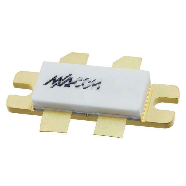
| 描述 | MOSFET RF N-CHAN PLD-1.5 |
| 产品分类 | RF FET |
| 品牌 | Freescale Semiconductor |
| 数据手册 | |
| 产品图片 |
|
| 产品型号 | MRF6V10010NR4 |
| PCN封装 | http://cache.freescale.com/files/shared/doc/pcn/PCN15687.htm |
| rohs | 无铅 / 符合限制有害物质指令(RoHS)规范要求 |
| 产品系列 | - |
| 产品目录页面 | |
| 供应商器件封装 | PLD-1.5 |
| 其它名称 | MRF6V10010NR4CT |
| 功率-输出 | 10W |
| 包装 | 剪切带 (CT) |
| 噪声系数 | - |
| 增益 | 25dB |
| 封装/外壳 | PLD-1.5 |
| 晶体管类型 | LDMOS |
| 标准包装 | 1 |
| 电压-测试 | 50V |
| 电压-额定 | 100V |
| 电流-测试 | 10mA |
| 频率 | 1.09GHz |
| 额定电流 | 2.5mA |


- 商务部:美国ITC正式对集成电路等产品启动337调查
- 曝三星4nm工艺存在良率问题 高通将骁龙8 Gen1或转产台积电
- 太阳诱电将投资9.5亿元在常州建新厂生产MLCC 预计2023年完工
- 英特尔发布欧洲新工厂建设计划 深化IDM 2.0 战略
- 台积电先进制程称霸业界 有大客户加持明年业绩稳了
- 达到5530亿美元!SIA预计今年全球半导体销售额将创下新高
- 英特尔拟将自动驾驶子公司Mobileye上市 估值或超500亿美元
- 三星加码芯片和SET,合并消费电子和移动部门,撤换高东真等 CEO
- 三星电子宣布重大人事变动 还合并消费电子和移动部门
- 海关总署:前11个月进口集成电路产品价值2.52万亿元 增长14.8%

PDF Datasheet 数据手册内容提取
Freescale Semiconductor DocumentNumber:MRF6V10010N Technical Data Rev.3,7/2010 RF Power Field Effect Transistor N--Channel Enhancement--Mode Lateral MOSFET MRF6V10010NR4 RFPowertransistordesignedforapplicationsoperatingatfrequencies between960and1400MHz,1%to20%dutycycle.Thisdeviceissuitablefor useinpulsedapplications. • TypicalPulsedPerformance:VDD=50Volts,IDQ=10mA,Pout=10Watts Peak(2WAvg.),f=1090MHz,PulseWidth=100μsec,DutyCycle=20% PowerGain(cid:151)25dB 1090MHz,10W,50V DrainEfficiency(cid:151)69% PULSED Features LATERALN--CHANNEL • CharacterizedwithSeriesEquivalentLarge--SignalImpedanceParameters RFPOWERMOSFET • QualifiedUptoaMaximumof50VDDOperation • IntegratedESDProtection • GreaterNegativeGate--SourceVoltageRangeforImprovedClassC Operation • RoHSCompliant • InTapeandReel.R4Suffix=100Unitsper12mm,7inchReel. CASE466--03,STYLE1 PLD--1.5 PLASTIC Table1.MaximumRatings Rating Symbol Value Unit Drain--SourceVoltage VDSS --0.5,+100 Vdc Gate--SourceVoltage VGS --6.0,+10 Vdc StorageTemperatureRange Tstg --65to+150 °C CaseOperatingTemperature TC 150 °C OperatingJunctionTemperature TJ 200 °C Table2.ThermalCharacteristics Characteristic Symbol Value(1,2) Unit ThermalResistance,JunctiontoCase CaseTemperature79°C,10WPulsed,100μsecPulseWidth,20%DutyCycle ZθJC 1.6 °C/W 1. MTTFcalculatoravailableathttp://www.freescale.com/rf.SelectSoftware&Tools/DevelopmentTools/CalculatorstoaccessMTTF calculatorsbyproduct. 2. RefertoAN1955,ThermalMeasurementMethodologyofRFPowerAmplifiers.Gotohttp://www.freescale.com/rf. SelectDocumentation/ApplicationNotes--AN1955. ©FreescaleSemiconductor,Inc.,2008--2010.Allrightsreserved. MRF6V10010NR4 RFDeviceData FreescaleSemiconductor 1
Table3.ESDProtectionCharacteristics TestMethodology Class HumanBodyModel(perJESD22--A114) 1C(Minimum) MachineModel(perEIA/JESD22--A115) A(Minimum) ChargeDeviceModel(perJESD22--C101) IV(Minimum) Table4.MoistureSensitivityLevel TestMethodology Rating PackagePeakTemperature Unit PerJESD22--A113,IPC/JEDECJ--STD--020 3 260 °C Table5.ElectricalCharacteristics (TA=25°Cunlessotherwisenoted) Characteristic Symbol Min Typ Max Unit OffCharacteristics Gate--SourceLeakageCurrent IGSS (cid:151) (cid:151) 10 μAdc (VGS=5Vdc,VDS=0Vdc) Drain--SourceBreakdownVoltage V(BR)DSS 100 (cid:151) (cid:151) Vdc (VGS=0Vdc,ID=7mA) ZeroGateVoltageDrainLeakageCurrent IDSS (cid:151) (cid:151) 50 μAdc (VDS=50Vdc,VGS=0Vdc) ZeroGateVoltageDrainLeakageCurrent IDSS (cid:151) (cid:151) 2.5 mA (VDS=100Vdc,VGS=0Vdc) OnCharacteristics GateThresholdVoltage VGS(th) 1 1.7 2.5 Vdc (VDS=10Vdc,ID=36μAdc) GateQuiescentVoltage VGS(Q) 1.7 2.4 3.2 Vdc (VDD=50Vdc,ID=10mAdc,MeasuredinFunctionalTest) Drain--SourceOn--Voltage VDS(on) (cid:151) 0.2 (cid:151) Vdc (VGS=10Vdc,ID=70mAdc) DynamicCharacteristics ReverseTransferCapacitance Crss (cid:151) 0.1 (cid:151) pF (VDS=50Vdc±30mV(rms)ac@1MHz,VGS=0Vdc) OutputCapacitance Coss (cid:151) 3.38 (cid:151) pF (VDS=50Vdc±30mV(rms)ac@1MHz,VGS=0Vdc) InputCapacitance Ciss (cid:151) 9.55 (cid:151) pF (VDS=50Vdc,VGS=0Vdc±30mV(rms)ac@1MHz) FunctionalTests(InFreescaleTestFixture,50ohmsystem)VDD=50Vdc,IDQ=10mA,Pout=10WPeak(2WAvg.),f=1090MHz, Pulsed,100μsecPulseWidth,20%DutyCycle PowerGain Gps 23 25 28 dB DrainEfficiency ηD 66 69 (cid:151) % InputReturnLoss IRL (cid:151) --12 --8 dB MRF6V10010NR4 RFDeviceData 2 FreescaleSemiconductor
L1 VBIAS VSUPPLY + C9 C8 C7 C13 C2 C3 C12 R1 L2 RF R2 C10 OUTPUT Z8 Z9 Z10 Z11 Z12 RF INPUT Z1 Z2 Z3 C5 Z4 C6 Z5 Z6 Z7 C14 C15 C11 C1 DUT C16 C4 Z1 0.200″x0.080″Microstrip Z8 0.367″x0.320″Microstrip Z2 0.696″x0.120″Microstrip Z9 0.162″x0.320″Microstrip Z3 0.087″x0.320″Microstrip Z10 0.757″x0.080″Microstip Z4 0.323″x0.320″Microstrip Z11 0.763″x0.080″Microstrip Z5 0.320″x0.620″x0.185″Taper Z12 0.290″x0.080″Microstrip Z6 0.135″x0.620″Microstrip PCB ArlonCuClad250GX--0300--55--22,0.030″,εr=2.55 Z7 0.714″x0.620″Microstrip Figure1.MR6V10010NR4TestCircuitSchematic Table6.MR6V10010NR4TestCircuitComponentDesignationsandValues Part Description PartNumber Manufacturer C1,C9,C12 43pFChipCapacitors ATC100B430JT500XT ATC C2 10μF,35VTantalumCapacitor T491D106K035AT Kemet C3,C8 2.2μF,100VChipCapacitors GQM1885C2A2R2CB01B Murata C4,C6 7.5pFChipCapacitors ATC100B7R5CT500XT ATC C5,C16 3.0pFChipCapacitors ATC100B3R0CT500XT ATC C7 0.1μFChipCapacitor C1206C104K5RACTR Kemet C10,C15 0.3pFChipCapacitors ATC100B0R3BT500XT ATC C11 5.6pFChipCapacitor ATC100B5R6CT500XT ATC C13 470μF,63VChipCapacitor 477KXM063M IlllinoisCapacitor C14 47pFChipCapacitor ATC100B470JT500XT ATC L1 8nHInductor A03TKLC Coilcraft L2 5nHInductor A02TKLC Coilcraft R1 3300Ω,1/4WChipResistor CRCW12063301FKEA Vishay R2 10Ω,1/4WChipResistor CRCW120610R0FKEA Vishay MRF6V10010NR4 RFDeviceData FreescaleSemiconductor 3
C7 L1 C3 C13 C2 C8 C12 R1 C9 R2 C16 C4 C15 L2 C14 C1 C5 C10 C6 C11 MRF6V10010N Rev.3 Figure2.MRF6V10010NR4TestCircuitComponentLayout MRF6V10010NR4 RFDeviceData 4 FreescaleSemiconductor
TYPICALCHARACTERISTICS 100 10 Measuredwith±30mV(rms)ac@1MHz VGS=0Vdc S) (pF) 10 Ciss (AMP TJ=200°C NCE ENT 1 TJ=175°C A R T R CAPACI 1 Coss AINCU TJ=150°C C, DR ,D I Crss TC=25°C 0.1 0.1 0 10 20 30 40 50 1 10 100 VDS,DRAIN--SOURCEVOLTAGE(VOLTS) VDS,DRAIN--SOURCEVOLTAGE(VOLTS) Figure3.CapacitanceversusDrain--SourceVoltage Figure4.DCSafeOperatingArea 27 75 45 P3dB=40.66dBm(11.65W) Ideal Gps D E 26 70 S %) UL (dB) CY( m)P P(110d.4B2=W4)0.18dBm WERGAIN 25 ηD 65 EFFICIEN OWER(dB 40 Actual G,POps 24 60 DRAIND, UTPUTP 23 VDD=50Vdc,IDQ=10mA,f=1090MHz 55 η P,Oout VPDulDse=W50idVthdc=,1ID0Q0μ=s1e0cm,DAu,tfy=C1y0c9le0=M2H0z% PulseWidth=100μsec,DutyCycle=20% 22 50 35 5 6 7 8 9 10 11 12 12 13 14 15 16 17 18 19 Pout,OUTPUTPOWER(WATTS)PULSED Pin,INPUTPOWER(dBm)PULSED Figure5.PulsedPowerGainandDrainEfficiency Figure6.PulsedOutputPowerversus versusOutputPower InputPower 27 14 D TC=--30_C E S 12 25 UL P 85_C B) S) 10 d T GAIN( 23 50V R(WAT 8 25_C R E OWE 21 45V POW 6 P 40V T VDD=50Vdc G,ps 35V UTPU 4 IfD=Q1=09100MmHAz 19 IDQ=10mA,f=1090MHz O VDD=30V PDuultsyeCWycidleth==2100%0μsec P,out 2 PDuultsyeCWycidleth==2100%0μsec 17 0 0 2 4 6 8 10 12 0 0.01 0.02 0.03 0.04 0.05 0.06 0.07 Pout,OUTPUTPOWER(WATTS)PULSED Pin,INPUTPOWER(WATTS)PULSED Figure7.PulsedPowerGainversus Figure8.PulsedOutputPowerversus OutputPower InputPower MRF6V10010NR4 RFDeviceData FreescaleSemiconductor 5
TYPICALCHARACTERISTICS 29 80 ηD 28 70 %) GAIN(dB) 2276 25_C TC=--30_C 6500 CIENCY( WER 25 40 EFFI G,POps 24 85_C Gps 30 DRAIND, η 23 VDD=50Vdc,IDQ=10mA,f=1090MHz 20 PulseWidth=100μsec,DutyCycle=20% 22 10 0 2 4 6 8 10 12 14 Pout,OUTPUTPOWER(WATTS)PULSED Figure9.PulsedPowerGainandDrainEfficiency versusOutputPower 109 108 S) R U O 107 H ( F T T M 106 105 90 110 130 150 170 190 210 230 250 TJ,JUNCTIONTEMPERATURE(°C) ThisabovegraphdisplayscalculatedMTTFinhourswhenthedevice isoperatedatVDD=50Vdc,Pout=10WPeak,PulseWidth=100μsec, DutyCycle=20%,andηD=69%. MTTFcalculatoravailableathttp://www.freescale.com/rf.Select Software&Tools/DevelopmentTools/CalculatorstoaccessMTTF calculatorsbyproduct. Figure10.MTTFversusJunctionTemperature MRF6V10010NR4 RFDeviceData 6 FreescaleSemiconductor
Zo=50Ω Zload f=1090MHz Zsource f=1090MHz VDD=50Vdc,IDQ=10mA,Pout=10WPeak f Zsource Zload MHz Ω Ω 1090 1.15+j8.96 13.47+j34.32 Zsource = Testcircuitimpedanceasmeasuredfrom gatetoground. Zload = Testcircuitimpedanceasmeasured fromdraintoground. Input Device Output Matching Under Matching Network Test Network Z Z source load Figure11.SeriesEquivalentSourceandLoadImpedance MRF6V10010NR4 RFDeviceData FreescaleSemiconductor 7
PACKAGEDIMENSIONS 0.146 A 3.71 F 0.095 2.41 3 0.115 2.92 B D 1 2 R L 0.115 2.92 0.020 0.51 4 N 0.35(0.89)X45_ 5_ inches K 10_DRAFT mm SOLDERFOOTPRINT Q U P INCHES MILLIMETERS ZONEV H C DIM MIN MAX MIN MAX Y Y E A 0.255 0.265 6.48 6.73 4 B 0.225 0.235 5.72 5.97 C 0.065 0.072 1.65 1.83 D 0.130 0.150 3.30 3.81 NOTES: E 0.021 0.026 0.53 0.66 1. INTERPRETDIMENSIONSANDTOLERANCES ZONEW PERASMEY14.5M,1984. F 0.026 0.044 0.66 1.12 1 2 2. CONTROLLINGDIMENSION:INCH G 0.050 0.070 1.27 1.78 3. RESINBLEED/FLASHALLOWABLEINZONEV,W, H 0.045 0.063 1.14 1.60 ANDX. J 0.160 0.180 4.06 4.57 K 0.273 0.285 6.93 7.24 STYLE1: L 0.245 0.255 6.22 6.48 PIN1.DRAIN N 0.230 0.240 5.84 6.10 3 2.GATE P 0.000 0.008 0.00 0.20 G S 34..SSOOUURRCCEE QR 00..025050 00..026130 15..4008 15..6303 ZONEX S 0.006 0.012 0.15 0.31 U 0.006 0.012 0.15 0.31 VIEWY--Y CASE466--03 ZONEV 0.000 0.021 0.00 0.53 ISSUED ZONEW 0.000 0.010 0.00 0.25 ZONEX 0.000 0.010 0.00 0.25 PLD--1.5 PLASTIC MRF6V10010NR4 RFDeviceData 8 FreescaleSemiconductor
PRODUCTDOCUMENTATIONANDSOFTWARE Refertothefollowingdocumentstoaidyourdesignprocess. ApplicationNotes • AN1955:ThermalMeasurementMethodologyofRFPowerAmplifiers EngineeringBulletins • EB212:UsingDataSheetImpedancesforRFLDMOSDevices Software • ElectromigrationMTTFCalculator ForSoftware,doaPartNumbersearchathttp://www.freescale.com,andselectthe(cid:147)PartNumber(cid:148)link.GototheSoftware& Toolstabonthepart(cid:146)sProductSummarypagetodownloadtherespectivetool. REVISIONHISTORY Thefollowingtablesummarizesrevisionstothisdocument. Revision Date Description 0 June2008 • InitialReleaseofDataSheet 1 Feb.2009 • CorrectedZsource, (cid:147)2.57--j7.33(cid:148)to(cid:147)1.15+j8.96(cid:148)andZload,(cid:147)14.10--j34.77(cid:148)to(cid:147)13.47+j34.32(cid:148)inFig.11, SeriesEquivalentSourceandLoadImpedancedatatableandreplotteddata,p.7 2 June2009 • ModifieddatasheettoreflectMSLratingchangefrom1to3asaresultofthestandardizationofpacking processasdescribedinProductandProcessChangeNotificationnumber,PCN13516,p.2 • AddedElectromigrationMTTFCalculatoravailabilitytoProductDocumentation,ToolsandSoftware,p.9 3 July2010 • ReportingofpulsedthermaldatanowshownusingtheZθJCsymbol,Table2,ThermalCharacteristics,p.1 • Correctederrorsmadeinthetranslationoftheprintedcircuitboardtotheschematic,Fig.1,TestCircuit SchematicandZlist,p.3 MRF6V10010NR4 RFDeviceData FreescaleSemiconductor 9
HowtoReachUs: HomePage: www.freescale.com WebSupport: http://www.freescale.com/support USA/EuropeorLocationsNotListed: FreescaleSemiconductor,Inc. TechnicalInformationCenter,EL516 2100EastElliotRoad Tempe,Arizona85284 1--800--521--6274or+1--480--768--2130 www.freescale.com/support Europe,MiddleEast,andAfrica: FreescaleHalbleiterDeutschlandGmbH Informationinthisdocumentisprovidedsolelytoenablesystemandsoftware TechnicalInformationCenter implementerstouseFreescaleSemiconductorproducts.Therearenoexpressor Schatzbogen7 81829Muenchen,Germany impliedcopyrightlicensesgrantedhereundertodesignorfabricateanyintegrated +441296380456(English) circuitsorintegratedcircuitsbasedontheinformationinthisdocument. +46852200080(English) +498992103559(German) FreescaleSemiconductorreservestherighttomakechangeswithoutfurthernoticeto +33169354848(French) anyproductsherein.FreescaleSemiconductormakesnowarranty,representationor www.freescale.com/support guaranteeregardingthesuitabilityofitsproductsforanyparticularpurpose,nordoes FreescaleSemiconductorassumeanyliabilityarisingoutoftheapplicationoruseof Japan: anyproductorcircuit,andspecificallydisclaimsanyandallliability,includingwithout FreescaleSemiconductorJapanLtd. Headquarters limitationconsequentialorincidentaldamages.(cid:147)Typical(cid:148)parametersthatmaybe ARCOTower15F providedinFreescaleSemiconductordatasheetsand/orspecificationscananddo 1--8--1,Shimo--Meguro,Meguro--ku, varyindifferentapplicationsandactualperformancemayvaryovertime.Alloperating Tokyo153--0064 parameters,including(cid:147)Typicals(cid:148),mustbevalidatedforeachcustomerapplicationby Japan customer(cid:146)stechnicalexperts.FreescaleSemiconductordoesnotconveyanylicense 0120191014or+81354379125 underitspatentrightsnortherightsofothers.FreescaleSemiconductorproductsare support.japan@freescale.com notdesigned,intended,orauthorizedforuseascomponentsinsystemsintendedfor surgicalimplantintothebody,orotherapplicationsintendedtosupportorsustainlife, Asia/Pacific: FreescaleSemiconductorChinaLtd. orforanyotherapplicationinwhichthefailureoftheFreescaleSemiconductorproduct ExchangeBuilding23F couldcreateasituationwherepersonalinjuryordeathmayoccur.ShouldBuyer No.118JianguoRoad purchaseoruseFreescaleSemiconductorproductsforanysuchunintendedor ChaoyangDistrict unauthorizedapplication,BuyershallindemnifyandholdFreescaleSemiconductor Beijing100022 anditsofficers,employees,subsidiaries,affiliates,anddistributorsharmlessagainstall China claims,costs,damages,andexpenses,andreasonableattorneyfeesarisingoutof, +861058798000 directlyorindirectly,anyclaimofpersonalinjuryordeathassociatedwithsuch support.asia@freescale.com unintendedorunauthorizeduse,evenifsuchclaimallegesthatFreescale Semiconductorwasnegligentregardingthedesignormanufactureofthepart. ForLiteratureRequestsOnly: FreescaleSemiconductorLiteratureDistributionCenter 1--800--441--2447or+1--303--675--2140 FreescaletandtheFreescalelogoaretrademarksofFreescaleSemiconductor,Inc. Fax:+1--303--675--2150 Allotherproductorservicenamesarethepropertyoftheirrespectiveowners. LDCForFreescaleSemiconductor@hibbertgroup.com ©FreescaleSemiconductor,Inc.2008--2010.Allrightsreserved. MRF6V10010NR4 DocumentNumber:MRF6V10010N RFDeviceData 1R0ev.3,7/2010 FreescaleSemiconductor
Mouser Electronics Authorized Distributor Click to View Pricing, Inventory, Delivery & Lifecycle Information: N XP: MRF6V10010NR4