ICGOO在线商城 > 分立半导体产品 > 晶体管 - FET,MOSFET - 射频 > BF991,215
 Datasheet下载
- 型号: BF991,215
- 制造商: NXP Semiconductors
- 库位|库存: xxxx|xxxx
- 要求:
| 数量阶梯 | 香港交货 | 国内含税 |
| +xxxx | $xxxx | ¥xxxx |
查看当月历史价格
查看今年历史价格
BF991,215产品简介:
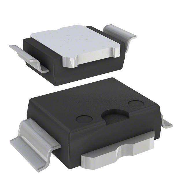
ICGOO电子元器件商城为您提供BF991,215由NXP Semiconductors设计生产,在icgoo商城现货销售,并且可以通过原厂、代理商等渠道进行代购。 BF991,215价格参考。NXP SemiconductorsBF991,215封装/规格:晶体管 - FET,MOSFET - 射频, 射频 Mosfet N 通道双门 10V 10mA 100MHz 29dB SOT-143B。您可以下载BF991,215参考资料、Datasheet数据手册功能说明书,资料中有BF991,215 详细功能的应用电路图电压和使用方法及教程。
NXP USA Inc. 的 BF991,215 是一款双栅极 N 沟道 MOSFET,属于射频场效应晶体管(RF FET),广泛应用于高频、低噪声的射频前端电路中。该器件具有良好的增益和噪声特性,适用于工作频率在数百MHz至数GHz范围内的场景。

典型应用场景包括:
1. 无线通信接收机前端放大器:BF991 常用于 FM 收音机、电视调谐器、短波接收设备等中的低噪声放大器(LNA),可有效提升信号接收灵敏度。
2. 高频混频器与变频电路:其双栅极结构使其适合用作射频混频器,实现信号频率转换,常见于广播接收和通信系统中。
3. 便携式与电池供电设备:由于功耗较低,BF991 适用于对功耗敏感的便携式无线电设备、无线麦克风接收器和遥控装置等。
4. 工业与消费类射频模块:可用于无线传感器、远程控制单元及小型发射机中,作为小信号放大或振荡电路元件。

BF991,215 封装小巧,便于集成在高密度PCB上,适合空间受限的应用。其稳定的射频性能和高可靠性,使其在模拟射频设计中仍具一定应用价值,尤其在成本敏感且无需极高频率的场合。尽管较新型器件不断涌现,BF991 在维修替换和传统设计中仍被广泛使用。
| 参数 | 数值 |
| 产品目录 | |
| 描述 | MOSFET NCH DUAL GATE 20V SOT143B射频MOSFET晶体管 N-CH DUAL GATE 20V VHF |
| 产品分类 | RF FET分离式半导体 |
| Id-ContinuousDrainCurrent | 0.02 A |
| Id-连续漏极电流 | 0.02 A |
| 品牌 | NXP Semiconductors |
| 产品手册 | |
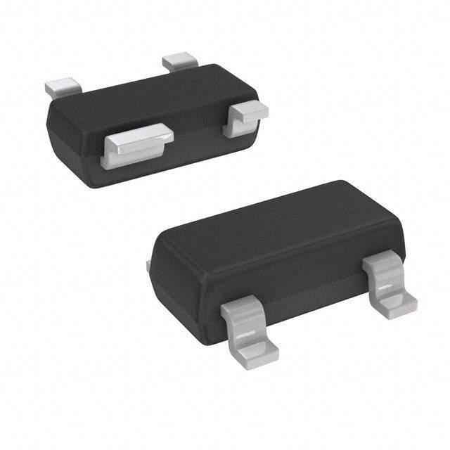
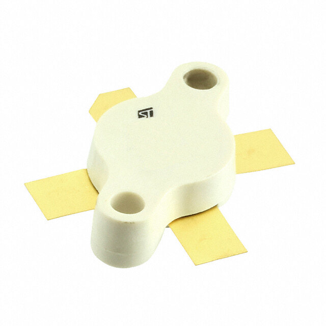
| 产品图片 |
|
| rohs | 符合RoHS无铅 / 符合限制有害物质指令(RoHS)规范要求 |
| 产品系列 | 晶体管,晶体管射频,射频MOSFET晶体管,NXP Semiconductors BF991,215- |
| 数据手册 | |
| 产品型号 | BF991,215 |
| PCN封装 | |
| PCN设计/规格 | |
| Pd-PowerDissipation | 200 mW |
| Pd-功率耗散 | 200 mW |
| Vds-Drain-SourceBreakdownVoltage | 20 V |
| Vds-漏源极击穿电压 | 20 V |
| Vgs-Gate-SourceBreakdownVoltage | 6 V |
| Vgs-栅源极击穿电压 | 6 V |
| 产品目录页面 | |
| 产品种类 | 射频MOSFET晶体管 |
| 产品类型 | RF MOSFET Small Signal |
| 供应商器件封装 | SOT-143B |
| 其它名称 | 568-1970-1 |
| 功率-输出 | - |
| 功率耗散 | 200 mW |
| 包装 | 剪切带 (CT) |
| 商标 | NXP Semiconductors |
| 噪声系数 | 0.7dB |
| 增益 | 29dB |
| 安装风格 | SMD/SMT |
| 封装 | Reel |
| 封装/外壳 | TO-253-4,TO-253AA |
| 封装/箱体 | SOT-143 |
| 工厂包装数量 | 3000 |
| 技术 | MOSFET |
| 晶体管极性 | N-Channel |
| 晶体管类型 | N 通道双门 |
| 最大工作温度 | + 150 C |
| 最小工作温度 | - 65 C |
| 标准包装 | 1 |
| 汲极/源极击穿电压 | 20 V |
| 漏极连续电流 | 0.02 A |
| 电压-测试 | 10V |
| 电压-额定 | 20V |
| 电流-测试 | 10mA |
| 配置 | Single Dual Gate |
| 闸/源击穿电压 | 6 V |
| 零件号别名 | BF991 T/R |
| 频率 | 100MHz |
| 额定电流 | 20mA |


- 商务部:美国ITC正式对集成电路等产品启动337调查
- 曝三星4nm工艺存在良率问题 高通将骁龙8 Gen1或转产台积电
- 太阳诱电将投资9.5亿元在常州建新厂生产MLCC 预计2023年完工
- 英特尔发布欧洲新工厂建设计划 深化IDM 2.0 战略
- 台积电先进制程称霸业界 有大客户加持明年业绩稳了
- 达到5530亿美元!SIA预计今年全球半导体销售额将创下新高
- 英特尔拟将自动驾驶子公司Mobileye上市 估值或超500亿美元
- 三星加码芯片和SET,合并消费电子和移动部门,撤换高东真等 CEO
- 三星电子宣布重大人事变动 还合并消费电子和移动部门
- 海关总署:前11个月进口集成电路产品价值2.52万亿元 增长14.8%


PDF Datasheet 数据手册内容提取
BF991 N-channel dual-gate MOS-FET Rev. 03 — 20 November 2007 Product data sheet IMPORTANT NOTICE Dear customer, As from October 1st, 2006 Philips Semiconductors has a new trade name -NXPSemiconductors,whichwillbeusedinfuturedatasheetstogetherwithnewcontact details. IndatasheetswherethepreviousPhilipsreferencesremain,pleaseusethenewlinksas shown below. http://www.philips.semiconductors.com use http://www.nxp.com http://www.semiconductors.philips.com use http://www.nxp.com (Internet) sales.addresses@www.semiconductors.philips.com use salesaddresses@nxp.com (email) The copyright notice at the bottom of each page (or elsewhere in the document, depending on the version) - © Koninklijke Philips Electronics N.V. (year). All rights reserved - is replaced with: - © NXP B.V. (year). All rights reserved. - If you have any questions related to the data sheet, please contact our nearest sales office via e-mail or phone (details via salesaddresses@nxp.com). Thank you for your cooperation and understanding, NXP Semiconductors
NXP Semiconductors Product specification N-channel dual-gate MOS-FET BF991 FEATURES DESCRIPTION • Protected against excessive input voltage surges by Depletion type field-effect transistor in a plastic SOT143 integrated back-to-back diodes between gates microminiature package with interconnected source and source. and substrate. APPLICATIONS • VHF applications such as: handbook, halfpage d 4 3 – VHF television tuners and FM tuners g – Professional communication equipment. 2 g 1 PINNING PIN SYMBOL DESCRIPTION 1 2 1 s, b source s,b 2 d drain Top view MAM039 3 g gate2 2 Marking code: %MA. 4 g gate1 1 Fig.1 Simplified outline (SOT143) and symbol. QUICK REFERENCE DATA SYMBOL PARAMETER CONDITIONS TYP. MAX. UNIT V drain-source voltage - 20 V DS I drain current - 20 mA D P total power dissipation up to T =60(cid:176) C - 200 mW tot amb T junction temperature - 150 (cid:176) C j Y transfer admittance f=1kHz; I =10mA; V =10V; V =4V 14 - mS fs D DS G2-S C input capacitance at gate1 f=1MHz; I =10mA; V =10V; V =4V 2.1 - pF ig1-s D DS G2-S C feedback capacitance f=1MHz; I =10mA; V =10V; V =4V 20 - fF rs D DS G2-S F noise figure f=200MHz; G =2mS; B =B ; 1 2 dB S S Sopt I =10mA; V =10V; V =4V D DS G2-S Rev. 03 - 20 November 2007 2 of 7
NXP Semiconductors Product specification N-channel dual-gate MOS-FET BF991 LIMITING VALUES In according with the Absolute Maximum Rating System (IEC134). SYMBOL PARAMETER CONDITIONS MIN. MAX. UNIT V drain-source voltage - 20 V DS I drain current (DC) - 20 mA D I average drain current - 20 mA D(AV) I gate1-source current - – 10 mA G1-S I gate2-source current - – 10 mA G2-S P total power dissipation up to T =60(cid:176) C; note1 - 200 mW tot amb T storage temperature - 65 +150 (cid:176) C stg T junction temperature - 150 (cid:176) C j THERMAL CHARACTERISTICS SYMBOL PARAMETER CONDITIONS VALUE UNIT R thermal resistance from junction to ambient in free air; note1 460 K/W thj-a Note to the Limiting values and the Thermal characteristics 1. Device mounted on a ceramic substrate of 8· 10· 0.7mm. MGE792 200 handbook, halfpage Ptot(cid:13) (mW) 100 0 0 100 200 Tamb (°C) Fig.2 Power derating curve. Rev. 03 - 20 November 2007 3 of 7
NXP Semiconductors Product specification N-channel dual-gate MOS-FET BF991 STATIC CHARACTERISTICS T =25(cid:176) C unless otherwise specified. j SYMBOL PARAMETER CONDITIONS MIN. MAX. UNIT I gate1 cut-off current V =5V; V =V =0 - 50 nA G1-SS G1-S G2-S DS I gate2 cut-off current V =5V; V =V =0 - 50 nA G2-SS G2-S G1-S DS I drain current V =10V; V =0; V =4V 4 25 mA DSS DS G1-S G2-S V gate1-source breakdown voltage I =10mA; V =V =0 6 20 V (BR)G1-SS G1-SS G2-S DS V gate2-source breakdown voltage I =10mA; V =V =0 6 20 V (BR)G2-SS G2-SS G1-S DS V gate1-source cut-off voltage I =20m A; V =10V; V =4V - - 2.5 V (P)G1-S D DS G2-S V gate2-source cut-off voltage I =20m A; V =10V; V =0 - - 2.5 V (P)G2-S D DS G1-S DYNAMIC CHARACTERISTICS Measuring conditions (common source): I =10mA; V =10V; V =4V; T =25(cid:176) C. D DS G2-S amb SYMBOL PARAMETER CONDITIONS MIN. TYP. MAX. UNIT Y transfer admittance f=1kHz 10 14 - mS fs C input capacitance at gate1 f=1MHz - 2.1 - pF ig1-s C input capacitance at gate2 f=1MHz - 1 - pF ig2-s C feedback capacitance f=1MHz - 20 - fF rs C output capacitance f=1MHz - 1.1 - pF os F noise figure f=100MHz; G =1mS; B =B - 0.7 1.7 dB S S Sopt f=200MHz; G =2mS; B =B - 1 2 dB S S Sopt G transducer gain; note1 f=100MHz; G =1mS; B =B ; - 29 - dB tr S S Sopt G =0.5mS; B =B L L Lopt f=200MHz; G =2mS; B =B ; - 26 - dB S S Sopt G =0.5mS; B =B L L Lopt Note 1. Crystal mounted in a SOT103 package. Rev. 03 - 20 November 2007 4 of 7
NXP Semiconductors Product specification N-channel dual-gate MOS-FET BF991 PACKAGE OUTLINE 3.0(cid:13) handbook, full pagewidth 2.8 B 0.150(cid:13) 0.75(cid:13) 0.090 1.9 A 0.2M A B 0.60 4 3 o 0.1(cid:13) 10(cid:13) max 1.4(cid:13) 2.5(cid:13) max 1.2 max o 10(cid:13) max 1 2 1.1(cid:13) max 30(cid:13)o 0(cid:13) 0(cid:13) 0.1M A B MBC845 0.88 0.48 max 0.1 0.1 1.7 TOP VIEW Dimensions in mm. See alsoSoldering recommendations. Fig.3 SOT143. Rev. 03 - 20 November 2007 5 of 7
BF991 NXP Semiconductors N-channel dual-gate MOS-FET Legal information Data sheet status Document status[1][2] Product status[3] Definition Objective [short] data sheet Development This document contains data from the objective specification for product development. Preliminary [short] data sheet Qualification This document contains data from the preliminary specification. Product [short] data sheet Production This document contains the product specification. [1] Please consult the most recently issued document before initiating or completing a design. [2] The term ‘short data sheet’ is explained in section “Definitions”. [3] Theproductstatusofdevice(s)describedinthisdocumentmayhavechangedsincethisdocumentwaspublishedandmaydifferincaseofmultipledevices.Thelatestproductstatus information is available on the Internet at URLhttp://www.nxp.com. Definitions malfunction of an NXP Semiconductors product can reasonably be expected to result in personal injury, death or severe property or environmental damage. NXP Semiconductors accepts no liability for inclusion and/or use of Draft —The document is a draft version only. The content is still under NXP Semiconductors products in such equipment or applications and internal review and subject to formal approval, which may result in therefore such inclusion and/or use is at the customer’s own risk. modifications or additions. NXP Semiconductors does not give any representations or warranties as to the accuracy or completeness of Applications —Applications that are described herein for any of these informationincludedhereinandshallhavenoliabilityfortheconsequencesof products are for illustrative purposes only. NXP Semiconductors makes no use of such information. representation or warranty that such applications will be suitable for the specified use without further testing or modification. Short data sheet —A short data sheet is an extract from a full data sheet withthesameproducttypenumber(s)andtitle.Ashortdatasheetisintended Limiting values —Stress above one or more limiting values (as defined in forquickreferenceonlyandshouldnotbereliedupontocontaindetailedand theAbsoluteMaximumRatingsSystemofIEC60134)maycausepermanent full information. For detailed and full information see the relevant full data damagetothedevice.Limitingvaluesarestressratingsonlyandoperationof sheet, which is available on request via the local NXP Semiconductors sales the device at these or any other conditions above those given in the office. In case of any inconsistency or conflict with the short data sheet, the Characteristics sections of this document is not implied. Exposure to limiting full data sheet shall prevail. values for extended periods may affect device reliability. Terms and conditions of sale —NXP Semiconductors products are sold Disclaimers subjecttothegeneraltermsandconditionsofcommercialsale,aspublished athttp://www.nxp.com/profile/terms, including those pertaining to warranty, intellectual property rights infringement and limitation of liability, unless General —Information in this document is believed to be accurate and explicitly otherwise agreed to in writing by NXP Semiconductors. In case of reliable.However,NXPSemiconductorsdoesnotgiveanyrepresentationsor any inconsistency or conflict between information in this document and such warranties,expressedorimplied,astotheaccuracyorcompletenessofsuch terms and conditions, the latter will prevail. information and shall have no liability for the consequences of use of such No offer to sell or license —Nothing in this document may be interpreted information. or construed as an offer to sell products that is open for acceptance or the Right to make changes —NXPSemiconductorsreservestherighttomake grant,conveyanceorimplicationofanylicenseunderanycopyrights,patents changes to information published in this document, including without or other industrial or intellectual property rights. limitation specifications and product descriptions, at any time and without notice.Thisdocumentsupersedesandreplacesallinformationsuppliedprior to the publication hereof. Trademarks Suitability for use —NXP Semiconductors products are not designed, Notice:Allreferencedbrands,productnames,servicenamesandtrademarks authorized or warranted to be suitable for use in medical, military, aircraft, are the property of their respective owners. space or life support equipment, nor in applications where failure or Contact information For additional information, please visit:http://www.nxp.com For sales office addresses, send an email to:salesaddresses@nxp.com Rev. 03 - 20 November 2007 6 of 7
BF991 NXP Semiconductors N-channel dual-gate MOS-FET Revision history Revision history Document ID Release date Data sheet status Change notice Supersedes BF991_N_3 20071120 Product data sheet - BF991_2 Modifications: • Fig. 1 on page 2; Figure note changed BF991_2 19910401 Product specification - BF991_SF_1 BF991_SF_1 - - - - Pleasebeawarethatimportantnoticesconcerningthisdocumentandtheproduct(s) described herein, have been included in section ‘Legal information’. © NXP B.V. 2007. All rights reserved. For more information, please visit: http://www.nxp.com For sales office addresses, please send an email to: salesaddresses@nxp.com Date of release: 20 November 2007 Document identifier: BF991_N_3