ICGOO在线商城 > 分立半导体产品 > 晶体管 - FET,MOSFET - 射频 > SD2933
 Datasheet下载
- 型号: SD2933
- 制造商: STMicroelectronics
- 库位|库存: xxxx|xxxx
- 要求:
| 数量阶梯 | 香港交货 | 国内含税 |
| +xxxx | $xxxx | ¥xxxx |
查看当月历史价格
查看今年历史价格
SD2933产品简介:
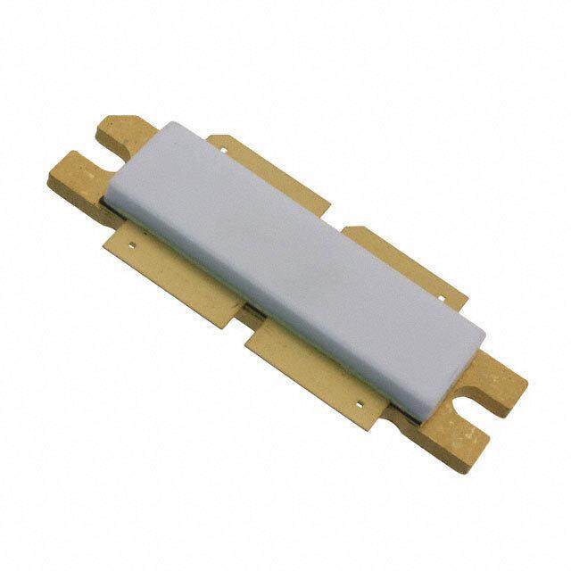
ICGOO电子元器件商城为您提供SD2933由STMicroelectronics设计生产,在icgoo商城现货销售,并且可以通过原厂、代理商等渠道进行代购。 SD2933价格参考。STMicroelectronicsSD2933封装/规格:晶体管 - FET,MOSFET - 射频, 射频 Mosfet N 通道 50V 250mA 30MHz 23.5dB 300W M177。您可以下载SD2933参考资料、Datasheet数据手册功能说明书,资料中有SD2933 详细功能的应用电路图电压和使用方法及教程。
STMicroelectronics的SD2933是一款射频(RF)晶体管,具体属于FET(场效应晶体管)和MOSFET(金属氧化物半导体场效应晶体管)类别。该器件主要用于高频和射频应用领域,具有低噪声、高增益和高线性度的特点,适用于多种无线通信设备和系统。

应用场景:

1. 射频放大器:
   SD2933常用于射频放大器中,特别是在低噪声放大器(LNA)和功率放大器(PA)的设计中。它能够提供出色的增益和线性度,确保信号在传输过程中不失真,并且保持较低的噪声水平。这使得它非常适合用于蜂窝基站、Wi-Fi路由器和其他无线通信设备中的射频前端模块。

2. 无线通信系统:
   在无线通信系统中,如5G基站、4G LTE基站、WiMAX等,SD2933可以作为关键组件来提升系统的性能。它的高频特性使其能够在GHz频段内高效工作,支持更高的数据传输速率和更远的传输距离。

3. 卫星通信:
   卫星通信设备对射频性能要求极高,SD2933凭借其优异的射频特性,可以在卫星地面站、卫星电话和其他卫星通信设备中发挥重要作用。它能够有效处理从卫星接收到的微弱信号,并将其放大到可处理的水平。

4. 雷达系统:
   雷达系统需要高性能的射频组件来实现精确的目标检测和跟踪。SD2933可用于雷达发射机和接收机中的射频放大器部分,确保雷达信号的高质量传输和接收,从而提高雷达系统的分辨率和探测精度。

5. 测试与测量设备:
   在射频测试与测量设备中,如频谱分析仪、网络分析仪等,SD2933可以用于构建高性能的射频前端,以确保测试结果的准确性和可靠性。它的低噪声特性和高线性度有助于提高测量精度,减少测试误差。

总之,SD2933以其卓越的射频性能,广泛应用于各种高频和无线通信领域,为现代通信技术的发展提供了有力支持。
| 参数 | 数值 |
| 产品目录 | |
| 描述 | TRANS RF N-CH HF/VHF/UHF M177 |
| 产品分类 | RF FET |
| 品牌 | STMicroelectronics |
| 数据手册 | |
| 产品图片 |
|
| 产品型号 | SD2933 |
| rohs | 无铅 / 符合限制有害物质指令(RoHS)规范要求 |
| 产品系列 | - |
| 产品目录页面 | |
| 供应商器件封装 | M177 |
| 其它名称 | 497-5469 |
| 其它有关文件 | http://www.st.com/web/catalog/sense_power/FM1987/CL1988/SC519/PF66090?referrer=70071840 |
| 功率-输出 | 300W |
| 包装 | 托盘 |
| 噪声系数 | - |
| 增益 | 23.5dB |
| 封装/外壳 | M177 |
| 晶体管类型 | N 通道 |
| 标准包装 | 25 |
| 电压-测试 | 50V |
| 电压-额定 | 125V |
| 电流-测试 | 250mA |
| 频率 | 30MHz |
| 额定电流 | 40A |


- 商务部:美国ITC正式对集成电路等产品启动337调查
- 曝三星4nm工艺存在良率问题 高通将骁龙8 Gen1或转产台积电
- 太阳诱电将投资9.5亿元在常州建新厂生产MLCC 预计2023年完工
- 英特尔发布欧洲新工厂建设计划 深化IDM 2.0 战略
- 台积电先进制程称霸业界 有大客户加持明年业绩稳了
- 达到5530亿美元!SIA预计今年全球半导体销售额将创下新高
- 英特尔拟将自动驾驶子公司Mobileye上市 估值或超500亿美元
- 三星加码芯片和SET,合并消费电子和移动部门,撤换高东真等 CEO
- 三星电子宣布重大人事变动 还合并消费电子和移动部门
- 海关总署:前11个月进口集成电路产品价值2.52万亿元 增长14.8%


PDF Datasheet 数据手册内容提取
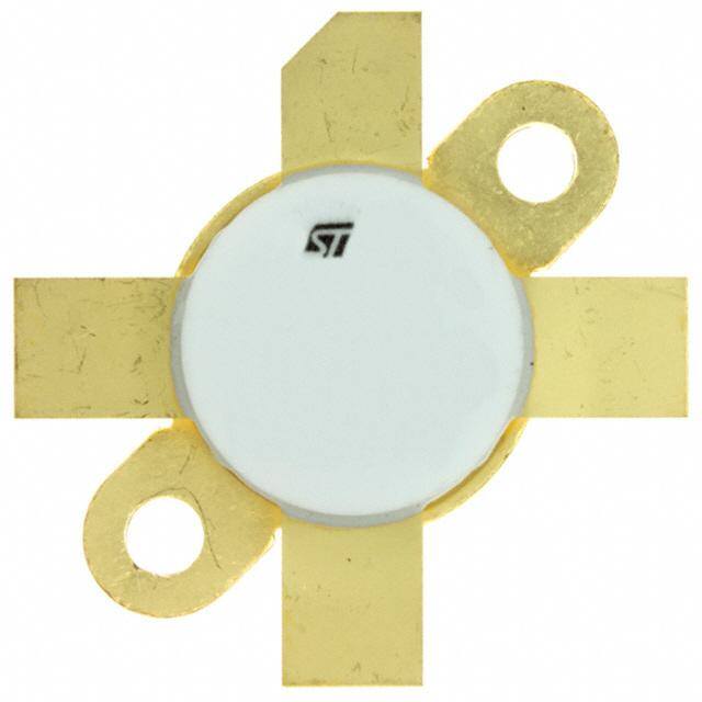
SD2933 HF/VHF/UHF RF power N-channel MOSFETs Datasheet - production data Features • Gold metalization • Excellent thermal stability • Common source configuration • P = 300 W min. with 20 dB gain @ 30 MHz OUT • Thermally enhanced packaging for lower junction temperatures M177 Epoxy sealed Description The SD2933 is a gold metalized N-channel MOS field-effect RF power transistor, intended for use Figure 1. Pin connection in 50 V dc large signal applications up to 150 MHz. Its special low thermal resistance package makes it ideal for ISM applications, where reliability and ruggedness are critical factors. 4 1 5 3 2 1. Drain 3. Gate 2. Source 4, 5. Source Table 1. Device summary Order code Marking Package Packaging SD2933W SD2933(1) M177 Plastic tray 1. For more details please refer to Chapter6: Marking, packing and shipping specifications. July 2016 DocID7193 Rev 15 1/16 This is information on a product in full production. www.st.com
Contents SD2933 Contents 1 Electrical data . . . . . . . . . . . . . . . . . . . . . . . . . . . . . . . . . . . . . . . . . . . . . . 3 1.1 Maximum rating . . . . . . . . . . . . . . . . . . . . . . . . . . . . . . . . . . . . . . . . . . . . . 3 1.2 Thermal data . . . . . . . . . . . . . . . . . . . . . . . . . . . . . . . . . . . . . . . . . . . . . . . 3 2 Electrical characteristics . . . . . . . . . . . . . . . . . . . . . . . . . . . . . . . . . . . . . 4 3 Impedance . . . . . . . . . . . . . . . . . . . . . . . . . . . . . . . . . . . . . . . . . . . . . . . . . 5 4 Typical performance (30 MHz) . . . . . . . . . . . . . . . . . . . . . . . . . . . . . . . . . 6 4.1 Test circuit (30 MHz) . . . . . . . . . . . . . . . . . . . . . . . . . . . . . . . . . . . . . . . . . . 9 5 Package information . . . . . . . . . . . . . . . . . . . . . . . . . . . . . . . . . . . . . . . . 12 6 Marking, packing and shipping specifications . . . . . . . . . . . . . . . . . . . 14 7 Revision history . . . . . . . . . . . . . . . . . . . . . . . . . . . . . . . . . . . . . . . . . . . 15 2/16 DocID7193 Rev 15
SD2933 Electrical data 1 Electrical data 1.1 Maximum rating T = 25 °C CASE Table 2. Absolute maximum ratings Symbol Parameter Value Unit V Drain source voltage 125 V (BR)DSS V Drain-gate voltage (R = 1MΩ) 125 V DGR GS V Gate-source voltage ±40 V GS I Drain current 40 A D P Power dissipation 648 W DISS Avalanche energy, single pulse E 1100 mJ AS (I = 53 A, 800 µH coil) D E (1) Avalanche energy, repetitive 50 mJ AR T Max. operating junction temperature 200 °C J T Storage temperature -65 to +150 °C STG 1. Repetitive rating: Pulse width limited by maximum junction temperature / repetitive avalanche causes additional power losses that can be calculated as: P = E * f AV AR 1.2 Thermal data Table 3. Thermal data Symbol Parameter Value Unit R Junction to case thermal resistance 0.27 °C/W thJ-C DocID7193 Rev 15 3/16 16
Electrical characteristics SD2933 2 Electrical characteristics T = 25 °C CASE Table 4. Static Symbol Test conditions Min. Typ. Max. Unit V V = 0 V I = 200 mA 125 V (BR)DSS GS DS I V = 0 V V = 50 V 100 µA DSS GS DS I V = 20 V V = 0 V 500 nA GSS GS DS V (1) V = 10 V I = 250 mA 1.5 4 V GS(Q) DS D V V = 10 V I = 20 A 3.0 V DS(ON) GS D G (1) V = 10 V I = 10 A see Table5: G sort mho FS DS D FS C V = 0 V V = 50 V f = 1 MHz 1000 pF ISS GS DS C V = 0 V V = 50 V f = 1 MHz 372 pF OSS GS DS C V = 0 V V = 50 V f = 1 MHz 29 pF RSS GS DS 1. V and G sorted with alpha/numeric code marked on unit. GS(Q) FS Table 5. G sort FS G sort Value FS A 10 - 10.99 B 11 - 11.99 C 12 - 12.99 D 13 - 13.99 E 14 - 14.99 F 15 - 15.99 G 16 - 16.99 H 17 - 18 Table 6. Dynamic Symbol Test Conditions Min. Typ. Max. Unit P V = 50 V I = 250 mA f = 30 MHz 300 400 W OUT DD DQ G V = 50 V I = 250 mA P = 300 W f = 30 MHz 20 23.5 dB PS DD DQ OUT η V = 50 V I = 250 mA P = 150 W f = 30 MHz 50 65 % D DD DQ OUT Load VDD = 50 V IDQ = 250 mA POUT = 300 W f = 30 MHz 3:1 VSWR mismatch all phase angles 4/16 DocID7193 Rev 15
SD2933 Impedance 3 Impedance Figure 2. Impedance data schematic D Z DL Typical Input Typical Drain Impedance Load Impedance G ZIN S Table 7. Impedance data f Z (Ω) Z (Ω) IN DL 30 MHz 1.8 - j 0.2 2.8 + j 2.3 108 MHz 1.9 + j 0.2 1.6 + j 1.4 175 MHz 1.9 + j 0.3 1.5 + j 1.6 DocID7193 Rev 15 5/16 16
Typical performance (30 MHz) SD2933 4 Typical performance (30 MHz) Figure 3. Capacitance vs. drain voltage Figure 4. Drain current vs. gate voltage 10000 15 f= 1 MHz Capacitance (pF) 1100000 CCCroissssss Id, Drain Current (A)105 Vdd=10V Tc = + 25oC TcT =c += 8- 02o0CoC 0 10 1 1.5 2 2.5 3 3.5 4 0 10 20 30 40 50 Vgs, Gate-Source Voltage (V) Vds, Drain Source Voltage (V) Figure 5. Gate-source voltage vs. case Figure 6. Maximum thermal resistance vs. case temperature temperature ED)1.15 0.33 Z MALI 1.1 Id= 12 A 0.32 OR Id= 10 A W) 0.31 E VOLTAGE (N01..90551 Id=.1 A Id= 15 AId= 7 A Id= 5 A RTH(j-c) (°C/00..022.893 RC 0.27 OU 0.9 Id= 4 A Id= 3 A 0.26 E-S Vdd= 10 V Id= 2 A 25 30 35 40 45 50 55 60 65 70 75 80 85 AT0.85 Id= 1 A Tc, CASE TEMPERATURE (°C) G Id=.25 A Vgs, 0.8-25 0 25 50 75 100 Tc, CASE TEMPERATURE (ºC) 6/16 DocID7193 Rev 15
SD2933 Typical performance (30 MHz) Figure 7. Transient thermal impedance 0.30 0.25 0.20 W C / g 0.15 e D h , Zt 0.10 0.05 0.00 1.E-05 1.E-04 1.E-03 1.E-02 1.E-01 1.E+00 1.E+01 Rectangular power pulse width (sec) single pulse 10% 20% 30% 40% 50% 60% 70% 80% 90% AM10216V1 Figure 8. Transient thermal impedance model PRC PRC1 R=.083 Ohm C=.0035904 F I_DC PRC Watts PRC2 R=.099 Ohm C=.1182727 F PRC PRC3 R=.088 Ohm C=2.4810922 F AAMM1100221177VV11 DocID7193 Rev 15 7/16 16
Typical performance (30 MHz) SD2933 Figure 9. Output power vs. input power Figure 10. Output power vs. input power (at different temperature) 500 500 W)400 Vdd= 50 V Tc= 25°C Tc= -20°C Pout, Output Power (123000000 fId=q 3V=02d 5dM0=Hm 4zA0 V out, Output Power (W)234000000 f= 30 MHz Tc= 80°C P100 Idq= 250 mA 0 Vdd= 50 V 0 0.3 0.6 0.9 1.2 1.5 1.8 2.1 2.4 2.7 0 Pin, Input Power ( W ) 0 0.3 0.6 0.9 1.2 1.5 1.8 2.1 2.4 2.7 Pin, Input Power (W) Figure 11. Power gain vs. output power Figure 12. Efficiency vs. output power 26 25 80 24 70 wer Gain (dB)222321 Efficiency (%)456000 f=30MHz o Vdd=50V P20 f= 30 MHz 30 Idq=250mA Idq= 250 mA 19 Vdd= 50 V 20 0 100 200 300 400 18 Pout, Output Power (W) 0 100 200 300 400 Pout, Output Power (W) Figure 13. Output power vs. supply voltage Figure 14. Output power vs. gate voltage 450 500 400 F= 30 MHz Tc= -20°C Power (W)330500 fId =q 3=0 2 M50H zmA Pin = 2.6 W Pin = 1.3 W OWER (W)340000 VIPddiqnd=== 2c 55o00n sVmtaAnt Tc= +25°C ut, Output 220500 Pin = 0.65 W OUTPUT P200 Tc= +80°C Po150 Pout, 100 100 24 26 28 30 32 34 36 38 40 42 44 46 48 50 0 Vdd, Supply Voltage (V) -3 -2 -1 0 1 2 3 Vgs, GATE-SOURCE VOLTAGE (V) 8/16 DocID7193 Rev 15
SD2933 Typical performance (30 MHz) 4.1 Test circuit (30 MHz) Figure 15. 30 MHz test circuit schematic Table 8. Transmission line dimensions Dim. Inch mm A 0.532 13.51 B 0.250 6.35 C 0.181 4.59 D 0.383 9.37 E 0.351 8.91 F 0.633 16.08 G 0.477 12.12 H 0.438 11.12 J 0.200 5.08 K 0.164 4.16 L 0.174 4.42 M 0.817 20.75 N 0.350 8.89 P 0.779 19.79 R 0.639 16.23 DocID7193 Rev 15 9/16 16
Typical performance (30 MHz) SD2933 Table 8. Transmission line dimensions (continued) Dim. Inch mm S 0.165 4.19 T 1.017 25.84 U 0.375 9.52 V 0.456 11.58 W 0.325 8.24 X 0.650 16.50 Table 9. 30 MHz test circuit part list Component Description C1,C9 0.01 μF / 500 V surface mount ceramic chip capacitor C2, C3 750 pF ATC 700B surface mount ceramic chip capacitor C4 300 pF ATC 700B surface mount ceramic chip capacitor C5,C10,C11,C14,C16 10000 pF ATC 200B surface mount ceramic chip capacitor C6 510 pF ATC 700B surface mount ceramic chip capacitor C7 300 pF ATC 700B surface mount ceramic chip capacitor C8 175-680 pF type 46 standard trimmer capacitor C12 47 μF / 63 V aluminum electrolytic radial lead capacitor C13 1200 pF ATC 700B surface mount ceramic chip capacitor C15 100 μF / 63 V aluminum electrolytic radial lead capacitor R1,R3 1 K OHM 1 W surface mount chip resistor R2 560 OHM 2 W wire-wound axis lead resistor T1 HF 2-30 MHz surface mount 9:1 transformer RG - 142B/U 50 OHM coaxial cable OD = 0.165[4.18] L 15”[381.00] T2 covered with 15”[381.00] tinned copper tubular brand 13/65” [5.1] width L1 1 3/4 turn air-wound 16 AWG ID = 0.219 [5.56] poly-coated magnet wire L2 1 3/4 turn air-wound 12 AWG ID = 0.250 [6.34] bus bar wire RFC1,RFC2 3 turns 14 AWG wire through ferrite toroid FB1 Surface mount EMI shield bead FB2 Toroid PCB ULTRALAM 2000. 0.030” THK, εr = 2.55, 2 Oz ED CU both sides 10/16 DocID7193 Rev 15
SD2933 Typical performance (30 MHz) Figure 16. 30 MHz test circuit photomaster s e h c n 4 i 6.4 inches Figure 17. 30 MHz test circuit DocID7193 Rev 15 11/16 16
Package information SD2933 5 Package information In order to meet environmental requirements, ST offers these devices in different grades of ECOPACK® packages, depending on their level of environmental compliance. ECOPACK® specifications, grade definitions and product status are available at: www.st.com. ECOPACK is an ST trademark. Figure 18. M177 package outline(a) a. Controlling dimensions in inches. 12/16 DocID7193 Rev 15
SD2933 Package information Table 10. M177 (.500 dia 4/L N/HERM W/FLG) package mechanical data mm Inch Dim. Min. Typ. Max. Min. Typ. Max. A 5.72 5.97 0.225 0.235 B 6.73 6.96 0.265 0.275 C 21.84 22.10 0.860 0.870 D 28.70 28.96 1.130 1.140 E 13.84 14.10 0.545 0.555 F 0.08 - 0.18 0.003 - 0.007 G 2.49 2.74 0.098 0.108 H 3.81 4.32 0.150 0.170 I 7.11 0.280 J 27.43 28.45 1.080 1.120 K 15.88 16.13 0.625 0.635 DocID7193 Rev 15 13/16 16
Marking, packing and shipping specifications SD2933 6 Marking, packing and shipping specifications Table 11. Packing and shipping specifications Pcs per Dry pack Order code Packaging GFS code Lot code tray humidity SD2933W Plastic tray 25 < 10% Not mixed Not mixed Figure 19. Marking layout for SD2933W Table 12. Marking specifications Symbol Description W Wafer process code X G sort FS CZ Assembly plant xxx Last 3 digits of diffusion lot VY Diffusion plant MAR Country of origin CZ Test and finishing plant y Assembly year yy Assembly week 14/16 DocID7193 Rev 15
SD2933 Revision history 7 Revision history Table 13. Document revision history Date Revision Changes 30-Jul-2004 9 Inserted Section6: Marking, packing and shipping specifications. 22-Sep-2011 10 Updated EAS in Table2: Absolute maximum ratings. Minor text changes to improve readability. 03-Oct-2011 11 Updated parameter Z in Table7: Impedance data. IN Inserted Figure7: Transient thermal impedance and Figure8: 17-Nov-2011 12 Transient thermal impedance model. 10-Jan-2012 13 Updated Figure7: Transient thermal impedance. – Added row for “Avalanche energy, repetitive” and footnote to 30-Sep-2013 14 Table2: Absolute maximum ratings – Minor text and formatting changes – Updated V in Table2: Absolute maximum ratings. 14-Jul-2016 15 GS – Minor text changes. DocID7193 Rev 15 15/16 16
SD2933 IMPORTANT NOTICE – PLEASE READ CAREFULLY STMicroelectronics NV and its subsidiaries (“ST”) reserve the right to make changes, corrections, enhancements, modifications, and improvements to ST products and/or to this document at any time without notice. Purchasers should obtain the latest relevant information on ST products before placing orders. ST products are sold pursuant to ST’s terms and conditions of sale in place at the time of order acknowledgement. Purchasers are solely responsible for the choice, selection, and use of ST products and ST assumes no liability for application assistance or the design of Purchasers’ products. No license, express or implied, to any intellectual property right is granted by ST herein. Resale of ST products with provisions different from the information set forth herein shall void any warranty granted by ST for such product. ST and the ST logo are trademarks of ST. All other product or service names are the property of their respective owners. Information in this document supersedes and replaces information previously supplied in any prior versions of this document. © 2016 STMicroelectronics – All rights reserved 16/16 DocID7193 Rev 15
Mouser Electronics Authorized Distributor Click to View Pricing, Inventory, Delivery & Lifecycle Information: S TMicroelectronics: SD2933 SD2933W