ICGOO在线商城 > 分立半导体产品 > 晶体管 - FET,MOSFET - 射频 > BF1108,215

 Datasheet下载
- 型号: BF1108,215
- 制造商: NXP Semiconductors
- 库位|库存: xxxx|xxxx
- 要求:
| 数量阶梯 | 香港交货 | 国内含税 |
| +xxxx | $xxxx | ¥xxxx |
查看当月历史价格
查看今年历史价格
BF1108,215产品简介:
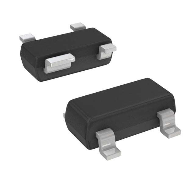
ICGOO电子元器件商城为您提供BF1108,215由NXP Semiconductors设计生产,在icgoo商城现货销售,并且可以通过原厂、代理商等渠道进行代购。 BF1108,215价格参考¥1.62-¥1.62。NXP SemiconductorsBF1108,215封装/规格:晶体管 - FET,MOSFET - 射频, 射频 Mosfet N 通道 SOT-143B。您可以下载BF1108,215参考资料、Datasheet数据手册功能说明书,资料中有BF1108,215 详细功能的应用电路图电压和使用方法及教程。
BF1108,215 是 NXP USA Inc. 生产的一款射频 MOSFET 晶体管,适用于高频射频(RF)信号处理。该器件主要用于以下应用场景:

1. 射频放大器:BF1108,215 常用于射频功率放大器中,适用于无线通信系统中的信号放大,如蜂窝通信基站、无线接入点等。

2. 高频通信设备:由于其良好的高频特性,该器件适用于 VHF、UHF 以及 L 波段等射频和微波通信设备中,用于信号传输和处理。

3. 广播发射设备:在广播电台、电视发射系统中,作为射频功率输出级,用于提升发射信号的强度,确保信号远距离传输。

4. 工业与测量设备:用于射频测试仪器、频谱分析仪、信号发生器等设备中,作为射频信号的放大或调制元件。

5. 航空航天与军事通信:因其稳定性和高频性能,也适用于对可靠性要求较高的军用通信系统和航空航天电子系统中。

该器件采用先进的 MOSFET 技术,具有高增益、低噪声和良好线性度的特点,适合用于需要高稳定性和高频率响应的射频应用场景。
| 参数 | 数值 |
| 产品目录 | |
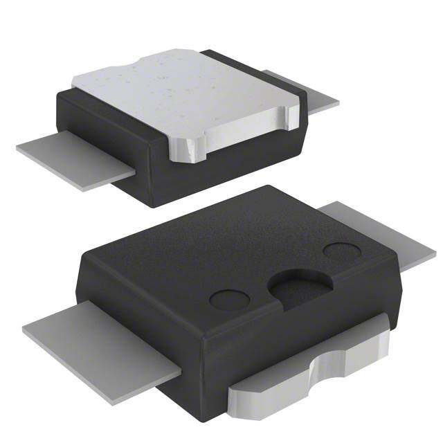
| 描述 | IC RF SWITCH SOT143BRF 开关 IC Single N-CH 7V 10mA 4 LEADS |
| 产品分类 | RF FET集成电路 - IC |
| 品牌 | NXP Semiconductors |
| 产品手册 | |
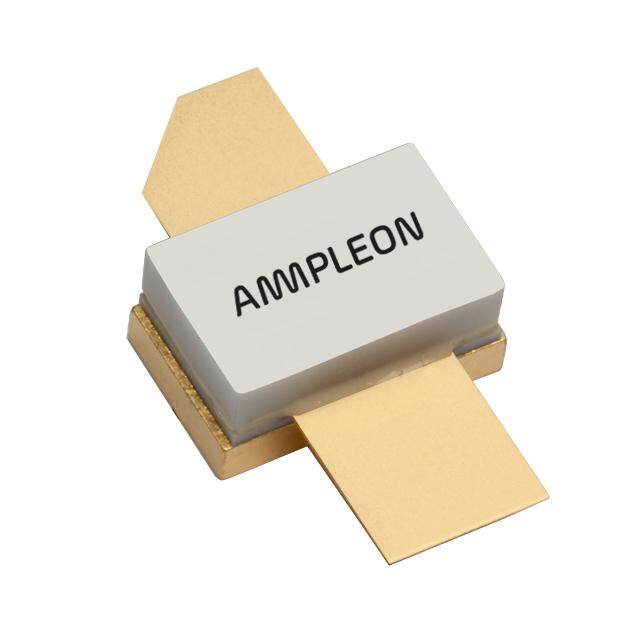
| 产品图片 |
|
| rohs | 符合RoHS无铅 / 符合限制有害物质指令(RoHS)规范要求 |
| 产品系列 | RF集成电路,RF 开关 IC,NXP Semiconductors BF1108,215- |
| 数据手册 | |
| 产品型号 | BF1108,215 |
| PCN封装 | |
| PCN设计/规格 | |
| 产品种类 | RF 开关 IC |
| 介入损耗 | 1.3 dB |
| 供应商器件封装 | SOT-143B |
| 关闭隔离—典型值 | 38 dB |
| 其它名称 | 568-6147-6 |
| 功率-输出 | - |
| 包装 | Digi-Reel® |
| 商标 | NXP Semiconductors |
| 噪声系数 | - |
| 增益 | - |
| 安装风格 | SMD/SMT |
| 导通电阻—最大值 | 20 Ohms |
| 封装 | Reel |
| 封装/外壳 | TO-253-4,TO-253AA |
| 封装/箱体 | SOT-143B |
| 工厂包装数量 | 3000 |
| 开关数量 | Single |
| 晶体管类型 | N 通道 |
| 最大工作温度 | + 150 C |
| 标准包装 | 1 |
| 电压-测试 | - |
| 电压-额定 | 3V |
| 电流-测试 | - |
| 频率 | - |
| 额定电流 | 10mA |
| 高控制电压 | 3 V |


- 商务部:美国ITC正式对集成电路等产品启动337调查
- 曝三星4nm工艺存在良率问题 高通将骁龙8 Gen1或转产台积电
- 太阳诱电将投资9.5亿元在常州建新厂生产MLCC 预计2023年完工
- 英特尔发布欧洲新工厂建设计划 深化IDM 2.0 战略
- 台积电先进制程称霸业界 有大客户加持明年业绩稳了
- 达到5530亿美元!SIA预计今年全球半导体销售额将创下新高
- 英特尔拟将自动驾驶子公司Mobileye上市 估值或超500亿美元
- 三星加码芯片和SET,合并消费电子和移动部门,撤换高东真等 CEO
- 三星电子宣布重大人事变动 还合并消费电子和移动部门
- 海关总署:前11个月进口集成电路产品价值2.52万亿元 增长14.8%


PDF Datasheet 数据手册内容提取
BF1108; BF1108R Silicon RF switches Rev. 04 — 29 May 2008 Product data sheet 1. Product profile 1.1 General description These switches are a combination of a depletion type Field-Effect Transistor (FET) and a band-switching diode in an SOT143B (BF1108) or SOT143R (BF1108R) package. The low loss and high isolation capabilities of these devices provide excellent RF switching functions. The gate of the MOSFET can be isolated from ground with the diode, resulting in low losses. Integrated diodes between gate and source and between gate and drain protect against excessive input voltage surges. CAUTION This device is sensitive to ElectroStatic Discharge (ESD). Therefore care should be taken during transport and handling. 1.2 Features n Specially designed for low loss RF switching up to 1 GHz 1.3 Applications n Various RF switching applications such as: u Passive loop through for VCR tuner u Transceiver switching 1.4 Quick reference data Table 1. Quick reference data Symbol Parameter Conditions Min Typ Max Unit L on-state insertion loss R =R =50W ;f£ 1GHz; [1] - - 2 dB ins(on) S L V =V =0V; I =0mA SK DK F ISL off-state isolation R =R =50W ; f£ 1GHz; 30 - - dB off S L V =V =5V; I =1mA SK DK F R drain-source on-state V =0V; I =1mA - 12 20 W DSon KS D resistance V gate-source pinch-off V =1V; I =20m A - - 3 - 4 V GS(p) DS D voltage [1] I =diode forward current. F
BF1108; BF1108R NXP Semiconductors Silicon RF switches 2. Pinning information Table 2. Pinning Pin Description Simplified outline Graphic symbol BF1108 (SOT143B) 1 FET gate; diode anode 4 3 4 3 2 diode cathode 3 source [1] 4 drain [1] 1 2 1 2 001aai042 BF1108R (SOT143R) 1 FET gate; diode anode 3 4 3 4 2 diode cathode 3 source [1] 4 drain [1] 2 1 2 1 001aai043 [1] Drain and source are interchangeable. 3. Ordering information Table 3. Ordering information Type number Package Name Description Version BF1108 - plastic surface-mounted package; 4 leads SOT143B BF1108R - plastic surface-mounted package; reverse pinning; SOT143R 4leads 4. Marking Table 4. Marking Type number Marking code BF1108 NGp BF1108R NHp BF1108_BF1108R_4 © NXP B.V. 2008. All rights reserved. Product data sheet Rev. 04 — 29 May 2008 2 of 10
BF1108; BF1108R NXP Semiconductors Silicon RF switches 5. Limiting values Table 5. Limiting values In accordance with the Absolute Maximum Rating System (IEC 60134). Symbol Parameter Conditions Min Max Unit FET V drain-source voltage - 3 V DS V source-drain voltage - 3 V SD V drain-gate voltage - 7 V DG V source-gate voltage - 7 V SG I drain current - 10 mA D Diode V reverse voltage - 35 V R I forward current - 100 mA F FET and diode T storage temperature - 65 +150 (cid:176) C stg T junction temperature - 150 (cid:176) C j 6. Thermal characteristics Table 6. Thermal characteristics Symbol Parameter Conditions Typ Unit R thermal resistance from junction [1] 250 K/W th(j-sp) to solder point [1] Soldering point of FET gate and diode anode lead. 7. Static characteristics Table 7. Static characteristics T = 25(cid:176) C unless otherwise specified. j Symbol Parameter Conditions Min Typ Max Unit FET V gate-source breakdown V =0V; I =0.1mA 7 - - V (BR)GSS DS GS voltage V gate-source pinch-off voltage V =1V; I =20m A - - 3 - 4 V GS(p) DS D I drain cut-off current V =- 5V; V =2V - - 10 m A DSX GS DS I gate leakage current V =- 5V; V =0V - - 100 nA GSS GS DS R drain-source on-state V =0V; I =1mA - 12 20 W DSon GS D resistance Diode V forward voltage I =10 mA - - 1 V F F I reverse current V =25V - - 50 nA R R V =20V; T =75(cid:176) C - - 1 m A R amb BF1108_BF1108R_4 © NXP B.V. 2008. All rights reserved. Product data sheet Rev. 04 — 29 May 2008 3 of 10
BF1108; BF1108R NXP Semiconductors Silicon RF switches 8. Dynamic characteristics Table 8. Dynamic characteristics Common cathode; T = 25(cid:176) C. amb Symbol Parameter Conditions Min Typ Max Unit FET and diode L on-state insertion loss V =V =0V; I =0mA [1] ins(on) SK DK F R =R =50W ; f£ 1GHz - - 2 dB S L R =R =50W ; f=1GHz - 1.3 - dB S L R =R =75W ; f£ 1GHz - - 3 dB S L ISL off-state isolation V =V =5V; I =1mA off SK DK F R =R =50W ; f£ 1GHz 30 - - dB S L R =R =50W ; f=1GHz - 38 - dB S L R =R =75W ; f£ 1GHz 30 - - dB S L R drain-source on-state V =0V; I =1mA - 12 20 W DSon KS D resistance C input capacitance f=1MHz [2] i V =V =5V; I =1mA - 1 - pF SK DK F V =V =0V; I =0mA - 0.65 0.9 pF SK DK F C output capacitance f=1MHz [2] o V =V =5V; I =1mA - 1 - pF SK DK F V =V =0V; I =0mA - 0.65 0.9 pF SK DK F Diode C diode capacitance f=1MHz; V =0V - 1.1 - pF d R r diode forward resistance I =2mA; f=100 MHz [3] - - 0.7 W D F [1] I =diode forward current. F [2] C is the series connection of C and C ; C is the series connection of C and C . i GS GK o GD GK [3] Guaranteed on AQL basis; inspection level S4, AQL 1.0. BF1108_BF1108R_4 © NXP B.V. 2008. All rights reserved. Product data sheet Rev. 04 — 29 May 2008 4 of 10
BF1108; BF1108R NXP Semiconductors Silicon RF switches mgs357 mgs358 0 0 Lins(on) ISLoff - 1 - 20 - 2 - 40 - 3 - 4 - 60 0 400 800 1200 0 400 800 1200 f (MHz) f (MHz) V = V = 0 V; R = R = 50W ; I = 0 mA (diode V = V = 5 V; R = R = 50W ; I = 1 mA (diode SK DK S L F SK DK S L F forward current). forward current). Measured in test circuit seeFigure3. Measured in test circuit seeFigure3. Fig 1. On-state insertion loss as a function of Fig 2. Off-state isolation as a function of frequency; frequency; typical values typical values V 1 nF 100 kW BF1108/BF1108R 47 kW 50 W 50 W input output 1 nF 1 nF 4.7 kW 100 kW V 1 nF mbl028 On-state: V=0V. Off-state: V=5V. Fig 3. Test circuit BF1108_BF1108R_4 © NXP B.V. 2008. All rights reserved. Product data sheet Rev. 04 — 29 May 2008 5 of 10
BF1108; BF1108R NXP Semiconductors Silicon RF switches 9. Package outline Plastic surface-mounted package; 4 leads SOT143B D B E A X y v M A HE e bp w M B 4 3 Q A A1 c 1 2 Lp b1 e1 detail X 0 1 2 mm scale DIMENSIONS (mm are the original dimensions) UNIT A mAa1x bp b1 c D E e e1 HE Lp Q v w y 1.1 0.48 0.88 0.15 3.0 1.4 2.5 0.45 0.55 mm 0.1 1.9 1.7 0.2 0.1 0.1 0.9 0.38 0.78 0.09 2.8 1.2 2.1 0.15 0.45 OUTLINE REFERENCES EUROPEAN ISSUE DATE VERSION IEC JEDEC JEITA PROJECTION 04-11-16 SOT143B 06-03-16 Fig 4. Package outline SOT143B BF1108_BF1108R_4 © NXP B.V. 2008. All rights reserved. Product data sheet Rev. 04 — 29 May 2008 6 of 10
BF1108; BF1108R NXP Semiconductors Silicon RF switches Plastic surface-mounted package; reverse pinning; 4 leads SOT143R D B E A X y v M A HE e bp w M B 3 4 Q A A1 c 2 1 Lp b1 e1 detail X 0 1 2 mm scale DIMENSIONS (mm are the original dimensions) UNIT A A1 bp b1 c D E e e1 HE Lp Q v w y max 1.1 0.48 0.88 0.15 3.0 1.4 2.5 0.55 0.45 mm 0.1 1.9 1.7 0.2 0.1 0.1 0.9 0.38 0.78 0.09 2.8 1.2 2.1 0.25 0.25 OUTLINE REFERENCES EUROPEAN ISSUE DATE VERSION IEC JEDEC JEITA PROJECTION 04-11-16 SOT143R SC-61AA 06-03-16 Fig 5. Package outline SOT143R BF1108_BF1108R_4 © NXP B.V. 2008. All rights reserved. Product data sheet Rev. 04 — 29 May 2008 7 of 10
BF1108; BF1108R NXP Semiconductors Silicon RF switches 10. Abbreviations Table 9. Abbreviations Acronym Description AQL Acceptable Quality Level MOSFET Metal-Oxide Semiconductor Field-Effect Transistor RF Radio Frequency S4 Special inspection level 4 VCR VideoCassette Recorder 11. Revision history Table 10. Revision history Document ID Release date Data sheet status Change notice Supersedes BF1108_BF1108R_4 20080529 Product data sheet - BF1108_1108R_3 Modifications: • The format of this data sheet has been redesigned to comply with the new identity guidelines of NXP Semiconductors. • Legal texts have been adapted to the new company name where appropriate. • Symbol notation has been adapted to comply with the current guidelines of NXP Semiconductors. BF1108_1108R_3 19991118 Product data sheet - BF1108_1108R_2 (939775006477) BF1108_1108R_2 19990819 Product data sheet - BF1108_1108R_1 (939775006073) BF1108_1108R_1 19990517 Preliminary specification - - (939775005899) BF1108_BF1108R_4 © NXP B.V. 2008. All rights reserved. Product data sheet Rev. 04 — 29 May 2008 8 of 10
BF1108; BF1108R NXP Semiconductors Silicon RF switches 12. Legal information 12.1 Data sheet status Document status[1][2] Product status[3] Definition Objective [short] data sheet Development This document contains data from the objective specification for product development. Preliminary [short] data sheet Qualification This document contains data from the preliminary specification. Product [short] data sheet Production This document contains the product specification. [1] Please consult the most recently issued document before initiating or completing a design. [2] The term ‘short data sheet’ is explained in section “Definitions”. [3] Theproductstatusofdevice(s)describedinthisdocumentmayhavechangedsincethisdocumentwaspublishedandmaydifferincaseofmultipledevices.Thelatestproductstatus information is available on the Internet at URLhttp://www.nxp.com. 12.2 Definitions damage. NXP Semiconductors accepts no liability for inclusion and/or use of NXP Semiconductors products in such equipment or applications and therefore such inclusion and/or use is at the customer’s own risk. Draft —The document is a draft version only. The content is still under internal review and subject to formal approval, which may result in Applications —Applications that are described herein for any of these modifications or additions. NXP Semiconductors does not give any products are for illustrative purposes only. NXP Semiconductors makes no representations or warranties as to the accuracy or completeness of representation or warranty that such applications will be suitable for the informationincludedhereinandshallhavenoliabilityfortheconsequencesof specified use without further testing or modification. use of such information. Limiting values —Stress above one or more limiting values (as defined in Short data sheet —A short data sheet is an extract from a full data sheet theAbsoluteMaximumRatingsSystemofIEC60134)maycausepermanent withthesameproducttypenumber(s)andtitle.Ashortdatasheetisintended damagetothedevice.Limitingvaluesarestressratingsonlyandoperationof forquickreferenceonlyandshouldnotbereliedupontocontaindetailedand the device at these or any other conditions above those given in the full information. For detailed and full information see the relevant full data Characteristics sections of this document is not implied. Exposure to limiting sheet, which is available on request via the local NXP Semiconductors sales values for extended periods may affect device reliability. office. In case of any inconsistency or conflict with the short data sheet, the Terms and conditions of sale —NXP Semiconductors products are sold full data sheet shall prevail. subjecttothegeneraltermsandconditionsofcommercialsale,aspublished athttp://www.nxp.com/profile/terms, including those pertaining to warranty, 12.3 Disclaimers intellectual property rights infringement and limitation of liability, unless explicitly otherwise agreed to in writing by NXP Semiconductors. In case of any inconsistency or conflict between information in this document and such General —Information in this document is believed to be accurate and terms and conditions, the latter will prevail. reliable.However,NXPSemiconductorsdoesnotgiveanyrepresentationsor No offer to sell or license —Nothing in this document may be interpreted warranties,expressedorimplied,astotheaccuracyorcompletenessofsuch or construed as an offer to sell products that is open for acceptance or the information and shall have no liability for the consequences of use of such grant,conveyanceorimplicationofanylicenseunderanycopyrights,patents information. or other industrial or intellectual property rights. Right to make changes —NXPSemiconductorsreservestherighttomake Quick reference data —The Quick reference data is an extract of the changes to information published in this document, including without product data given in the Limiting values and Characteristics sections of this limitation specifications and product descriptions, at any time and without document, and as such is not complete, exhaustive or legally binding. notice.Thisdocumentsupersedesandreplacesallinformationsuppliedprior to the publication hereof. Suitability for use —NXP Semiconductors products are not designed, 12.4 Trademarks authorized or warranted to be suitable for use in medical, military, aircraft, space or life support equipment, nor in applications where failure or Notice:Allreferencedbrands,productnames,servicenamesandtrademarks malfunction of an NXP Semiconductors product can reasonably be expected are the property of their respective owners. to result in personal injury, death or severe property or environmental 13. Contact information For more information, please visit:http://www.nxp.com For sales office addresses, please send an email to:salesaddresses@nxp.com BF1108_BF1108R_4 © NXP B.V. 2008. All rights reserved. Product data sheet Rev. 04 — 29 May 2008 9 of 10
BF1108; BF1108R NXP Semiconductors Silicon RF switches 14. Contents 1 Product profile. . . . . . . . . . . . . . . . . . . . . . . . . . 1 1.1 General description. . . . . . . . . . . . . . . . . . . . . . 1 1.2 Features . . . . . . . . . . . . . . . . . . . . . . . . . . . . . . 1 1.3 Applications . . . . . . . . . . . . . . . . . . . . . . . . . . . 1 1.4 Quick reference data. . . . . . . . . . . . . . . . . . . . . 1 2 Pinning information. . . . . . . . . . . . . . . . . . . . . . 2 3 Ordering information. . . . . . . . . . . . . . . . . . . . . 2 4 Marking. . . . . . . . . . . . . . . . . . . . . . . . . . . . . . . . 2 5 Limiting values. . . . . . . . . . . . . . . . . . . . . . . . . . 3 6 Thermal characteristics. . . . . . . . . . . . . . . . . . . 3 7 Static characteristics. . . . . . . . . . . . . . . . . . . . . 3 8 Dynamic characteristics . . . . . . . . . . . . . . . . . . 4 9 Package outline . . . . . . . . . . . . . . . . . . . . . . . . . 6 10 Abbreviations. . . . . . . . . . . . . . . . . . . . . . . . . . . 8 11 Revision history. . . . . . . . . . . . . . . . . . . . . . . . . 8 12 Legal information. . . . . . . . . . . . . . . . . . . . . . . . 9 12.1 Data sheet status . . . . . . . . . . . . . . . . . . . . . . . 9 12.2 Definitions. . . . . . . . . . . . . . . . . . . . . . . . . . . . . 9 12.3 Disclaimers. . . . . . . . . . . . . . . . . . . . . . . . . . . . 9 12.4 Trademarks. . . . . . . . . . . . . . . . . . . . . . . . . . . . 9 13 Contact information. . . . . . . . . . . . . . . . . . . . . . 9 14 Contents. . . . . . . . . . . . . . . . . . . . . . . . . . . . . . 10 Pleasebeawarethatimportantnoticesconcerningthisdocumentandtheproduct(s) described herein, have been included in section ‘Legal information’. © NXP B.V. 2008. All rights reserved. For more information, please visit: http://www.nxp.com For sales office addresses, please send an email to: salesaddresses@nxp.com Date of release: 29 May 2008 Document identifier: BF1108_BF1108R_4