ICGOO在线商城 > 分立半导体产品 > 晶体管 - FET,MOSFET - 阵列 > NTJD1155LT1G
 Datasheet下载
- 型号: NTJD1155LT1G
- 制造商: ON Semiconductor
- 库位|库存: xxxx|xxxx
- 要求:
| 数量阶梯 | 香港交货 | 国内含税 |
| +xxxx | $xxxx | ¥xxxx |
查看当月历史价格
查看今年历史价格
NTJD1155LT1G产品简介:
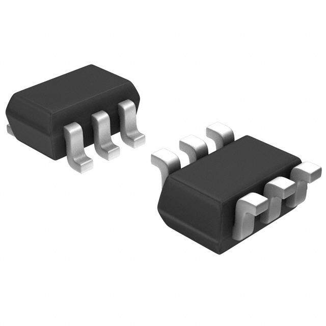
ICGOO电子元器件商城为您提供NTJD1155LT1G由ON Semiconductor设计生产,在icgoo商城现货销售,并且可以通过原厂、代理商等渠道进行代购。 NTJD1155LT1G价格参考。ON SemiconductorNTJD1155LT1G封装/规格:晶体管 - FET,MOSFET - 阵列, Mosfet Array N and P-Channel 8V 1.3A 400mW Surface Mount SC-88/SC70-6/SOT-363。您可以下载NTJD1155LT1G参考资料、Datasheet数据手册功能说明书,资料中有NTJD1155LT1G 详细功能的应用电路图电压和使用方法及教程。
ON Semiconductor(安森美)的NTJD1155LT1G是一款P沟道MOSFET阵列器件,内部集成两个相同的P沟道MOSFET,采用小型化封装(如SOT-23),适用于空间受限的便携式电子设备。该器件主要应用于需要低功耗、高效率开关控制的场景。

典型应用场景包括:
1. 电源管理:用于电池供电设备中的负载开关或电源通断控制,如智能手机、平板电脑和可穿戴设备,实现对不同模块的供电使能与节能管理。
2. 信号切换:在多路信号路径中作为模拟开关使用,适用于音频、数据线路的选择与隔离。
3. 电平转换电路:配合N沟道MOSFET构建无电感的电平移位电路,用于不同电压域之间的逻辑信号转换,常见于I²C、GPIO等数字接口中。
4. LED背光驱动:在中小尺寸显示屏中用于控制LED背光的开启与关闭。
5. 热插拔与过流保护辅助控制:与其他保护器件配合,实现电路的软启动和断路控制。

NTJD1155LT1G具有低阈值电压、低导通电阻(RDS(on))和高可靠性,适合3.3V或5V系统中使用。其封装小巧,便于高密度PCB布局,广泛应用于消费电子、工业控制、通信模块及便携式医疗设备等领域。
| 参数 | 数值 |
| 产品目录 | |
| ChannelMode | Enhancement |
| 描述 | MOSFET N/P-CH 8V 1.3A SOT-363MOSFET 8V +/-1.3A P-Channel w/Level Shift |
| 产品分类 | FET - 阵列分离式半导体 |
| FET功能 | 标准 |
| FET类型 | N 和 P 沟道 |
| Id-ContinuousDrainCurrent | +/- 1.3 A |
| Id-连续漏极电流 | 1.3 A |
| 品牌 | ON Semiconductor |
| 产品手册 | |
| 产品图片 |
|
| rohs | 符合RoHS无铅 / 符合限制有害物质指令(RoHS)规范要求 |
| 产品系列 | 晶体管,MOSFET,ON Semiconductor NTJD1155LT1G- |
| 数据手册 | |
| 产品型号 | NTJD1155LT1G |
| Pd-PowerDissipation | 0.4 W |
| Pd-功率耗散 | 400 mW |
| RdsOn-Drain-SourceResistance | 260 mOhms |
| RdsOn-漏源导通电阻 | 260 mOhms |
| Vds-Drain-SourceBreakdownVoltage | - 8 V |
| Vds-漏源极击穿电压 | - 8 V |
| Vgs-Gate-SourceBreakdownVoltage | 1 V |
| Vgs-栅源极击穿电压 | 1 V |
| 不同Id时的Vgs(th)(最大值) | 1V @ 250µA |
| 不同Vds时的输入电容(Ciss) | - |
| 不同Vgs时的栅极电荷(Qg) | - |
| 不同 Id、Vgs时的 RdsOn(最大值) | 175 毫欧 @ 1.2A,4.5V |
| 产品目录页面 | |
| 产品种类 | MOSFET |
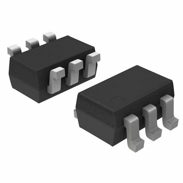
| 供应商器件封装 | SC-88/SC70-6/SOT-363 |
| 其它名称 | NTJD1155LT1GOSCT |
| 功率-最大值 | 400mW |
| 功率耗散 | 0.4 W |
| 包装 | 剪切带 (CT) |
| 商标 | ON Semiconductor |
| 安装类型 | 表面贴装 |
| 安装风格 | SMD/SMT |
| 导通电阻 | 260 mOhms |
| 封装 | Reel |
| 封装/外壳 | 6-TSSOP,SC-88,SOT-363 |
| 封装/箱体 | SC-88-6 |
| 工厂包装数量 | 3000 |
| 晶体管极性 | P-Channel |
| 最大工作温度 | + 150 C |
| 最小工作温度 | - 55 C |
| 标准包装 | 1 |
| 汲极/源极击穿电压 | - 8 V |
| 漏极连续电流 | +/- 1.3 A |
| 漏源极电压(Vdss) | 8V |
| 电流-连续漏极(Id)(25°C时) | 1.3A |
| 系列 | NTJD1155L |
| 通道模式 | Enhancement |
| 配置 | Dual |
| 闸/源击穿电压 | 1 V |


PDF Datasheet 数据手册内容提取
NTJD1155L Power MOSFET (cid:2) 8 V, 1.3 A, High Side Load Switch with Level−Shift, P−Channel SC−88 The NTJD1155L integrates a P and N−Channel MOSFET in a single package. This device is particularly suited for portable electronic equipment where low control signals, low battery voltages and high hhttttpp::////oonnsseemmii..ccoomm load currents are needed. The P−Channel device is specifically designed as a load switch using ON Semiconductor state−of−the−art V(BR)DSS RDS(on) TYP ID MAX trench technology. The N−Channel, with an external resistor (R1), 130 m(cid:4) @ −4.5 V functions as a level−shift to drive the P−Channel. The N−Channel 8.0 V 170 m(cid:4) @ −2.5 V ±1.3 A MOSFET has internal ESD protection and can be driven by logic 260 m(cid:4) @ −1.8 V signals as low as 1.5 V. The NTJD1155L operates on supply lines from 1.8 to 8.0 V and can drive loads up to 1.3 A with 8.0 V applied to both SIMPLIFIED SCHEMATIC V and V IN ON/OFF. 4 2,3 Features • Extremely Low RDS(on) P−Channel Load Switch MOSFET Q2 • 6 Level Shift MOSFET is ESD Protected • Low Profile, Small Footprint Package • VIN Range 1.8 to 8.0 V 5 Q1 • ON/OFF Range 1.5 to 8.0 V • These Devices are Pb−Free and are RoHS Compliant 1 MAXIMUM RATINGS (TJ = 25°C unless otherwise noted) MARKING SC−88 DIAGRAM Rating Symbol Value Unit (SOT−363) Input Voltage (VDSS, P−Ch) VIN 8.0 V 1 CASE 419B STYLE 30 TB M(cid:2) ON/OFF Voltage (VGS, N−Ch) VON/OFF 8.0 V (cid:2) Continuous Load Current Steady TA = 25°C IL ±1.3 A TB = Device Code (Note 1) State M = Date Code 1 TA = 85°C ±0.9 (cid:2) = Pb−Free Package Power Dissipation Steady TA = 25°C PD 0.40 W (Note: Microdot may be in either location) (Note 1) State TA = 85°C 0.20 Pulsed Load Current tp = 10 (cid:2)s ILM ±3.9 A PIN ASSIGNMENT Operating Junction and Storage Temperature TJ, −55 to °C D1/G2 G1 S2 TSTG 150 6 5 4 Source Current (Body Diode) IS −0.4 A Lead Temperature for Soldering Purposes TL 260 °C (1/8″ from case for 10 s) THERMAL CHARACTERISTICS 1 2 3 S1 D2 D2 Characteristic Symbol Max Unit Junction−to−Ambient – Steady State (Note 1) R(cid:3)JA 320 °C/W ORDERING INFORMATION Junction−to−Foot – Steady State (Note 1) R(cid:3)JF 220 Device Package Shipping† Stresses exceeding Maximum Ratings may damage the device. Maximum Ratings are stress ratings only. Functional operation above the Recommended NTJD1155LT1G SC−88 3000/Tape & Reel Operating Conditions is not implied. Extended exposure to stresses above the (Pb−Free) Recommended Operating Conditions may affect device reliability. 1. Surface−mounted on FR4 board using 1 inch sq pad size †For information on tape and reel specifications, (Cu area = 1.127 in sq [1 oz] including traces). including part orientation and tape sizes, please refer to our Tape and Reel Packaging Specification Brochure, BRD8011/D. © Semiconductor Components Industries, LLC, 2012 1 Publication Order Number: November, 2012 − Rev. 5 NTJD1155L/D
NTJD1155L ELECTRICAL CHARACTERISTICS (TJ = 25°C unless otherwise noted) Characteristic Symbol Test Condition Min Typ Max Unit OFF CHARACTERISTICS Q2 Drain−to−Source Breakdown Voltage VIN VGS2 = 0 V, ID2 = 250 (cid:2)A −8.0 V Forward Leakage Current IFL VGS1 = 0 V, TJ = 25°C 1.0 (cid:2)A VDS2 = −8.0 V TJ = 125°C 10 Q1 Gate−to−Source Leakage Current IGSS VDS1 = 0 V, VGS1 = ±8.0 V ±100 nA Q1 Diode Forward On−Voltage VSD IS = −0.4 A, VGS1 = 0 V −0.8 −1.1 V ON CHARACTERISTICS ON/OFF Voltage VON/OFF 1.5 8.0 V Q1 Gate Threshold Voltage VGS1(th) VGS1 = VDS1, ID = 250 (cid:2)A 0.4 1.0 V Input Voltage VIN VGS1 = VDS1, ID = 250 (cid:2)A 1.8 8.0 V Q2 Drain−to−Source On Resistance RDS(on) VON/OFF = 1.5 V VIN = 4.5 V 130 175 m(cid:4) IL = 1.2 A VIN = 2.5 V 170 220 IL = 1.0 A VIN = 1.8 V 260 320 IL = 0.7 A Load Current IL VDROP ≤ 0.2 V, VIN = 5.0 V, 1.0 A VON/OFF = 1.5 V VDROP ≤ 0.3 V, VIN = 2.5 V, 1.0 VON/OFF = 1.5 V 4 2,3 VIN VOUT Q2 R1 C1 6 6 ON/OFF 5 CO LOAD Q1 1 CI R2 R2 GND Figure 1. Load Switch Application Components Description Values R1 Pullup Resistor Typical 10 k(cid:4) to 1.0 M(cid:4)* R2 Optional Slew−Rate Control Typical 0 to 100 k(cid:4)* CO, CI Output Capacitance Usually < 1.0 (cid:2)F C1 Optional In−Rush Current Control Typical ≤ 1000 pF *Minimum R1 value should be at least 10 x R2 to ensure Q1 turn−on. http://onsemi.com 2
NTJD1155L TYPICAL PERFORMANCE CURVES (TJ = 25°C unless otherwise noted) 0.70 0.50 0.65 0.45 0.60 0.55 0.40 0.50 0.35 0.45 TJ = 125°C TJ = 125°C (V)OP00..4305 (V)OP00..2350 R R D0.30 D V 0.25 TJ = 25°C V 0.20 TJ = 25°C 0.20 0.15 0.15 0.10 0.10 0.05 0.05 0 0 0 0.5 1.0 1.5 2.0 2.5 3.0 0 0.5 1.0 1.5 2.0 2.5 3.0 IL (AMPS) IL (AMPS) Figure 2. V vs. I @ V = 2.5 V Figure 3. V vs. I @ V = 4.5 V drop L in drop L in (cid:4)) (cid:4)) E ( 0.8 E ( 0.31 NC 0.7 IL = 1 A NC IL = 1 A Vin = 1.8 V TA VON/OFF = 1.5 to 8 V TA 0.26 VON/OFF = 1.5 to 8 V S S SI 0.6 SI RE RE 0.21 E 0.5 E C C UR 0.4 UR 0.16 O O S S − 0.3 − TO TO 0.11 Vin = 5 V N− 0.2 TJ = 125°C N− AI AI 0.06 R 0.1 R D n), 0.0 TJ = 25°C D n),0.01 o o S( 1.0 2.0 3.0 4.0 5.0 6.0 7.0 8.0 S( −50 −25 0 25 50 75 100 125 150 D D R VIN (VOLTS) R TJ, JUNCTION TEMPERATURE (°C) Figure 4. On−Resistance vs. Input Voltage Figure 5. On−Resistance Variation with Temperature 1.7 44 IL = 1 A 40 IL = 1 A RCEZED) 1.5 VON/OFF = 1.5 to 8 V 36 VCOi =N /1O0F F(cid:2) F= 1.5 V OUALI 32 Co = 1 (cid:2)F tr DRAIN−TO−S DS(on),ESISTANCE (NORM 110...319 Vin =V 5in V= 1.8 V (cid:2)TIME (s) 21212886420 td(off) tf RR 4 td(on) 0.7 0 −50 −25 0 25 50 75 100 125 150 0 1 2 3 4 5 6 7 8 TJ, JUNCTION TEMPERATURE (°C) R2 (k(cid:4)) Figure 6. Normalized On−Resistance Variation Figure 7. Switching Variation with Temperature R2 @ V = 4.5 V, R1 = 20 k(cid:2) in http://onsemi.com 3
NTJD1155L TYPICAL PERFORMANCE CURVES (TJ = 25°C unless otherwise noted) 22 40 20 36 IL = 1 A td(off) VON/OFF = 1.5 V 18 32 Ci = 10 (cid:2)F tr 16 Co = 1 (cid:2)F tf 28 14 s) s) 24 (cid:2)E ( 12 (cid:2)E ( 20 TIM 10 IL = 1 A TIM 16 86 VCoi n=/o 1ff0 = (cid:2) 3F V 12 tf td(on) Co = 1 (cid:2)F tr 8 4 2 td(on) 4 td(off) 0 0 0 1 2 3 4 5 6 7 8 0 1 2 3 4 5 6 7 8 R2 (k(cid:4)) R2 (k(cid:4)) Figure 8. Switching Variation Figure 9. Switching Variation R2 @ Vin = 4.5 V, R1 = 20 k(cid:2) R2 @ Vin = 2.5 V, R1 = 20 k(cid:2) 12 10 tf 8 s) IL = 1 A td(off) (cid:2) ME ( 6 VCoi n=/o 1ff0 = (cid:2) 3F V TI Co = 1 (cid:2)F tr 4 2 td(on) 0 0 1 2 3 4 5 6 7 8 R2 (k(cid:4)) Figure 10. Switching Variation R2 @ V = 2.5 V, R1 = 20 k(cid:2) E in S N O P 10 S RE Normalized to R(cid:3)JA at Steady State ( 1 inch pad) L A M R E 1 D = 0.5 H T T N 0.2 E P(pk) SI 0.1 R(cid:3)JC(t) = r(t) R(cid:3)JC AN 0.1 0.05 D CURVES APPLY FOR POWER R 0.02 PULSE TRAIN SHOWN T E 0.01 t1 READ TIME AT t1 TIV SINGLE PULSE t2 TJ(pk) − TC = P(pk) R(cid:3)JC(t) FEC 0.01 DUTY CYCLE, D = t1/t2 F 0.001 0.01 0.1 1 10 100 1000 E r(t), SQUARE WAVE PULSE DURATION TIME t, (s) Figure 11. FET Thermal Response http://onsemi.com 4
NTJD1155L PACKAGE DIMENSIONS SC−88 (SOT−363) CASE 419B−02 ISSUE W D NOTES: 1. DIMENSIONING AND TOLERANCING PER ANSI e Y14.5M, 1982. 2. CONTROLLING DIMENSION: INCH. 3. 419B−01 OBSOLETE, NEW STANDARD 419B−02. MILLIMETERS INCHES 6 5 4 DIM MIN NOM MAX MIN NOM MAX HE −E− AA1 00..8000 00..9055 10..1100 00..003010 00..003072 00..004034 1 2 3 A3 0.20 REF 0.008 REF b 0.10 0.21 0.30 0.004 0.008 0.012 C 0.10 0.14 0.25 0.004 0.005 0.010 D 1.80 2.00 2.20 0.070 0.078 0.086 E 1.15 1.25 1.35 0.045 0.049 0.053 b6 PL e 0.65 BSC 0.026 BSC 0.2 (0.008) M E M L 0.10 0.20 0.30 0.004 0.008 0.012 HE 2.00 2.10 2.20 0.078 0.082 0.086 A3 STYLE 30: PIN 1.SOURCE 1 2.DRAIN 2 C 3.DRAIN 2 A 4.SOURCE 2 5.GATE 1 6.DRAIN 1 A1 L SOLDERING FOOTPRINT* 0.50 0.0197 0.65 0.025 0.65 0.025 0.40 0.0157 1.9 0.0748 (cid:2) mm (cid:3) SCALE 20:1 inches *For additional information on our Pb−Free strategy and soldering details, please download the ON Semiconductor Soldering and Mounting Techniques Reference Manual, SOLDERRM/D. ON Semiconductor and are registered trademarks of Semiconductor Components Industries, LLC (SCILLC). SCILLC owns the rights to a number of patents, trademarks, copyrights, trade secrets, and other intellectual property. A listing of SCILLC’s product/patent coverage may be accessed at www.onsemi.com/site/pdf/Patent−Marking.pdf. SCILLC reserves the right to make changes without further notice to any products herein. SCILLC makes no warranty, representation or guarantee regarding the suitability of its products for any particular purpose, nor does SCILLC assume any liability arising out of the application or use of any product or circuit, and specifically disclaims any and all liability, including without limitation special, consequential or incidental damages. “Typical” parameters which may be provided in SCILLC data sheets and/or specifications can and do vary in different applications and actual performance may vary over time. All operating parameters, including “Typicals” must be validated for each customer application by customer’s technical experts. SCILLC does not convey any license under its patent rights nor the rights of others. SCILLC products are not designed, intended, or authorized for use as components in systems intended for surgical implant into the body, or other applications intended to support or sustain life, or for any other application in which the failure of the SCILLC product could create a situation where personal injury or death may occur. Should Buyer purchase or use SCILLC products for any such unintended or unauthorized application, Buyer shall indemnify and hold SCILLC and its officers, employees, subsidiaries, affiliates, and distributors harmless against all claims, costs, damages, and expenses, and reasonable attorney fees arising out of, directly or indirectly, any claim of personal injury or death associated with such unintended or unauthorized use, even if such claim alleges that SCILLC was negligent regarding the design or manufacture of the part. SCILLC is an Equal Opportunity/Affirmative Action Employer. This literature is subject to all applicable copyright laws and is not for resale in any manner. PUBLICATION ORDERING INFORMATION LITERATURE FULFILLMENT: N. American Technical Support: 800−282−9855 Toll Free ON Semiconductor Website: www.onsemi.com Literature Distribution Center for ON Semiconductor USA/Canada P.O. Box 5163, Denver, Colorado 80217 USA Europe, Middle East and Africa Technical Support: Order Literature: http://www.onsemi.com/orderlit Phone: 303−675−2175 or 800−344−3860 Toll Free USA/Canada Phone: 421 33 790 2910 Fax: 303−675−2176 or 800−344−3867 Toll Free USA/Canada Japan Customer Focus Center For additional information, please contact your local Email: orderlit@onsemi.com Phone: 81−3−5817−1050 Sales Representative http://onsemi.com NTJD1155L/D 5
Mouser Electronics Authorized Distributor Click to View Pricing, Inventory, Delivery & Lifecycle Information: O N Semiconductor: NTJD1155LT1G