ICGOO在线商城 > 分立半导体产品 > 晶体管 - FET,MOSFET - 阵列 > SI1967DH-T1-GE3

 Datasheet下载
- 型号: SI1967DH-T1-GE3
- 制造商: Vishay
- 库位|库存: xxxx|xxxx
- 要求:
| 数量阶梯 | 香港交货 | 国内含税 |
| +xxxx | $xxxx | ¥xxxx |
查看当月历史价格
查看今年历史价格
SI1967DH-T1-GE3产品简介:
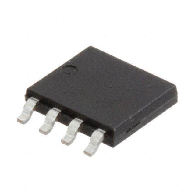
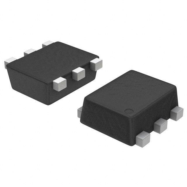
ICGOO电子元器件商城为您提供SI1967DH-T1-GE3由Vishay设计生产,在icgoo商城现货销售,并且可以通过原厂、代理商等渠道进行代购。 SI1967DH-T1-GE3价格参考。VishaySI1967DH-T1-GE3封装/规格:晶体管 - FET,MOSFET - 阵列, 2 个 P 沟道(双) Mosfet 阵列 20V 1.3A 1.25W 表面贴装 SC-70-6(SOT-363)。您可以下载SI1967DH-T1-GE3参考资料、Datasheet数据手册功能说明书,资料中有SI1967DH-T1-GE3 详细功能的应用电路图电压和使用方法及教程。
Vishay Siliconix的SI1967DH-T1-GE3是一款双通道N沟道增强型MOSFET阵列,广泛应用于各种需要高效开关和低导通电阻的场景。以下是其主要应用场景:

 1. 电源管理
   SI1967DH-T1-GE3常用于电源管理系统中,例如DC-DC转换器、电压调节模块(VRM)和负载开关。其低导通电阻(Rds(on))特性有助于减少功率损耗,提高效率。在这些应用中,MOSFET阵列可以作为高效的开关元件,控制电流的流动,确保电源系统的稳定性和可靠性。

 2. 电机驱动
   在小型电机驱动电路中,SI1967DH-T1-GE3可以用于驱动步进电机、直流电机或无刷电机。由于其快速的开关速度和低导通电阻,能够有效降低功耗,提升电机的响应速度和精度。此外,该器件的双通道设计允许同时控制两个电机或多个负载,简化了电路设计。

 3. 电池保护
   在电池管理系统(BMS)中,SI1967DH-T1-GE3可用于过流保护、短路保护和过温保护等。通过精确控制MOSFET的导通和关断,可以防止电池过充或过放,延长电池寿命。其低导通电阻也有助于减少电池内部的发热,提高安全性。

 4. 信号切换
   在通信设备、音频设备和其他需要高频信号切换的应用中,SI1967DH-T1-GE3可以作为信号路径的开关。其快速的开关特性和低电容使得它能够在高频条件下保持良好的性能,适用于高速数据传输和信号处理。

 5. 消费电子
   在智能手机、平板电脑、笔记本电脑等消费电子产品中,SI1967DH-T1-GE3常用于电源管理和外围设备接口的控制。例如,它可以用于USB端口的电源控制,确保设备在连接时能够安全地获取电力,同时避免过载和短路。

 6. 工业自动化
   在工业控制系统中,SI1967DH-T1-GE3可用于驱动传感器、执行器和其他低功率设备。其双通道设计允许同时控制多个设备,简化了工业自动化系统的设计和维护。

总之,SI1967DH-T1-GE3凭借其低导通电阻、快速开关速度和双通道设计,适用于多种高效能、低功耗的应用场景,特别是在电源管理、电机驱动和电池保护等领域表现出色。
| 参数 | 数值 |
| 产品目录 | |
| 描述 | MOSFET 2P-CH 20V 1.3A SC70-6MOSFET 20V 1.3A DUAL P-CH MOSFET |
| 产品分类 | FET - 阵列分离式半导体 |
| FET功能 | 逻辑电平门 |
| FET类型 | 2 个 P 沟道(双) |
| Id-连续漏极电流 | 1.3 A |
| 品牌 | Vishay / SiliconixVishay Siliconix |
| 产品手册 | http://www.vishay.com/doc?68784 |
| 产品图片 |
|
| rohs | 符合RoHS无铅 / 符合限制有害物质指令(RoHS)规范要求 |
| 产品系列 | 晶体管,MOSFET,Vishay / Siliconix SI1967DH-T1-GE3TrenchFET® |
| 数据手册 | |
| 产品型号 | SI1967DH-T1-GE3SI1967DH-T1-GE3 |
| Pd-PowerDissipation | 1.25 W |
| Pd-功率耗散 | 1.25 W |
| Qg-GateCharge | 2.6 nC |
| Qg-栅极电荷 | 2.6 nC |
| RdsOn-漏源导通电阻 | 490 mOhms |
| Vds-漏源极击穿电压 | - 20 V |
| Vgs-Gate-SourceBreakdownVoltage | +/- 8 V |
| Vgs-栅源极击穿电压 | 8 V |
| 不同Id时的Vgs(th)(最大值) | 1V @ 250µA |
| 不同Vds时的输入电容(Ciss) | 110pF @ 10V |
| 不同Vgs时的栅极电荷(Qg) | 4nC @ 8V |
| 不同 Id、Vgs时的 RdsOn(最大值) | 490 毫欧 @ 910mA,4.5V |
| 产品种类 | MOSFET |
| 供应商器件封装 | SC-70-6 (SOT-363) |
| 其它名称 | SI1967DH-T1-GE3CT |
| 功率-最大值 | 1.25W |
| 包装 | 剪切带 (CT) |
| 商标 | Vishay / Siliconix |
| 安装类型 | 表面贴装 |
| 安装风格 | SMD/SMT |
| 导通电阻 | 490 mOhms |
| 封装 | Reel |
| 封装/外壳 | 6-TSSOP,SC-88,SOT-363 |
| 封装/箱体 | SC-70-6 |
| 工厂包装数量 | 3000 |
| 晶体管极性 | P-Channel |
| 最大工作温度 | + 150 C |
| 最小工作温度 | - 55 C |
| 标准包装 | 1 |
| 正向跨导-最小值 | 2 S |
| 汲极/源极击穿电压 | 20 V |
| 漏极连续电流 | 1.3 A |
| 漏源极电压(Vdss) | 20V |
| 电流-连续漏极(Id)(25°C时) | 1.3A |
| 系列 | SI19xxDx |
| 配置 | Dual |
| 零件号别名 | SI1903DL-T1-GE3 |


- 商务部:美国ITC正式对集成电路等产品启动337调查
- 曝三星4nm工艺存在良率问题 高通将骁龙8 Gen1或转产台积电
- 太阳诱电将投资9.5亿元在常州建新厂生产MLCC 预计2023年完工
- 英特尔发布欧洲新工厂建设计划 深化IDM 2.0 战略
- 台积电先进制程称霸业界 有大客户加持明年业绩稳了
- 达到5530亿美元!SIA预计今年全球半导体销售额将创下新高
- 英特尔拟将自动驾驶子公司Mobileye上市 估值或超500亿美元
- 三星加码芯片和SET,合并消费电子和移动部门,撤换高东真等 CEO
- 三星电子宣布重大人事变动 还合并消费电子和移动部门
- 海关总署:前11个月进口集成电路产品价值2.52万亿元 增长14.8%
.jpg)


PDF Datasheet 数据手册内容提取
Si1967DH Vishay Siliconix Dual P-Channel 20 V (D-S) MOSFET FEATURES PRODUCT SUMMARY (cid:129) Halogen-free According to IEC 61249-2-21 V (V) R (Ω) I (A) Q (Typ.) DS DS(on) D g Definition 0.490 at VGS = - 4.5 V - 1.3a (cid:129) TrenchFET® Power MOSFET - 20 0.640 at VGS = - 2.5 V - 1.2 1.6 nC (cid:129) PWM Optimized (cid:129) Compliant to RoHS Directive 2002/95/EC 0.790 at VGS = - 1.8 V - 1.0 APPLICATIONS SOT-363 SC-70 (6-LEADS) (cid:129) Load Switch for Portable Devices S1 S2 S1 1 6 D1 Marking Code G1 2 5 G2 DF XXYY Lot Traceability G1 G2 and Date Code D2 3 4 S2 Part # Code Top View Ordering Information: S i1967DH-T1-E3 (Lead (Pb)-free) D1 D2 Si1967DH-T1-GE3 (Lead (Pb)-free and Halogen-free) P-Channel MOSFET P-Channel MOSFET ABSOLUTE MAXIMUM RATINGS T = 25 °C, unless otherwise noted A Parameter Symbol Limit Unit Drain-Source Voltage V - 20 DS V Gate-Source Voltage V ± 8 GS T = 25 °C - 1.3a C T = 70 °C - 1.1 C Continuous Drain Current (T = 150 °C) I J T = 25 °C D - 1.0b, c A T = 70 °C - 0.83b, c A A Pulsed Drain Current I - 3 DM T = 25 °C - 1 C Continuous Source-Drain Diode Current T = 25 °C IS - 0.6b, c A TC = 25 °C 1.25 TC = 70 °C 0.8 Maximum Power Dissipation P W T = 25 °C D 0.74b, c A T = 70 °C 0.47b, c A Operating Junction and Storage Temperature Range TJ, Tstg - 55 to 150 °C THERMAL RESISTANCE RATINGS Parameter Symbol Typical Maximum Unit Maximum Junction-to-Ambientb, d t ≤ 5 s RthJA 130 170 °C/W Maximum Junction-to-Foot (Drain) Steady State RthJF 80 100 Notes: a. Package limited. b. Surface mounted on 1" x 1" FR4 board. c. t = 5 s. d. Maximum under steady state conditions is 220 °C/W. Document Number: 68784 www.vishay.com S10-0721-Rev. B, 29-Mar-10 1
Si1967DH Vishay Siliconix SPECIFICATIONS T = 25 °C, unless otherwise noted J Parameter Symbol Test Conditions Min. Typ. Max. Unit Static Drain-Source Breakdown Voltage V V = 0 V, I = - 250 µA - 20 V DS GS D V Temperature Coefficient ΔV /T - 20 DS DS J I = - 250 µA mV/°C D V Temperature Coefficient ΔV /T 2 GS(th) GS(th) J Gate-Source Threshold Voltage V V = V , I = - 250 µA - 0.4 - 1.0 V GS(th) DS GS D Gate-Source Leakage I V = 0 V, V = ± 8 V ± 100 nA GSS DS GS V = - 20 V, V = 0 V - 1 DS GS Zero Gate Voltage Drain Current I µA DSS V = - 20 V, V = 0 V, T = 85 °C - 10 DS GS J On-State Drain Currenta I V ≤ - 5 V, V = - 4.5 V - 3 A D(on) DS GS V = - 4.5 V, I = - 0.91 A 0.390 0.490 GS D Drain-Source On-State Resistancea R V = - 2.5 V, I = - 0.8 A 0.500 0.640 Ω DS(on) GS D V = - 1.8 V, I = - 0.25 A 0.640 0.790 GS D Forward Transconductancea g V = - 10 V, I = - 0.91 A 2 S fs DS D Dynamicb Input Capacitance C 110 iss Output Capacitance C V = - 10 V, V = 0 V, f = 1 MHz 26 pF oss DS GS Reverse Transfer Capacitance C 16 rss V = - 10 V, V = - 8 V, I = - 1.1 A 2.6 4.0 DS GS D Total Gate Charge Q g 1.6 2.4 nC Gate-Source Charge Q V = - 10 V, V = - 4.5 V, I = - 1.1 A 0.36 gs DS GS D Gate-Drain Charge Q 0.33 gd Gate Resistance R f = 1 MHz 7.5 Ω g Turn-On Delay Time t 12 20 d(on) Rise Time tr VDD = - 10 V, RL = 12 Ω 27 40 Turn-Off Delay Time td(off) ID ≅ - 0.83 A, VGEN = - 4.5 V, Rg = 1 Ω 15 25 Fall Time t 10 15 f ns Turn-On Delay Time t 2 5 d(on) Rise Time tr VDD = - 10 V, RL = 12 Ω 12 20 Turn-Off Delay Time td(off) ID ≅ - 0.83 A, VGEN = - 8 V, Rg = 1 Ω 12 20 Fall Time t 10 15 f Drain-Source Body Diode Characteristics Continuous Source-Drain Diode Current I T = 25 °C - 1.0 S C A Pulse Diode Forward Currenta I - 3.0 SM Body Diode Voltage V I = - 0.9 A - 0.8 - 1.2 V SD S Body Diode Reverse Recovery Time t 25 50 ns rr Body Diode Reverse Recovery Charge Q 15 30 nC rr I = - 0.83 A, dI/dt = 100 A/µs, T = 25 °C F J Reverse Recovery Fall Time t 12 a ns Reverse Recovery Rise Time t 13 b Notes: a. Pulse test; pulse width ≤ 300 µs, duty cycle ≤ 2 % b. Guaranteed by design, not subject to production testing. Stresses beyond those listed under “Absolute Maximum Ratings” may cause permanent damage to the device. These are stress ratings only, and functional operation of the device at these or any other conditions beyond those indicated in the operational sections of the specifications is not implied. Exposure to absolute maximum rating conditions for extended periods may affect device reliability. www.vishay.com Document Number: 68784 2 S10-0721-Rev. B, 29-Mar-10
Si1967DH Vishay Siliconix TYPICAL CHARACTERISTICS 25°C, unless otherwise noted 3.0 1.0 VGS=5Vthru2.5V 2.5 0.8 Current(A) 12..50 VGS=2V Current(A) 0.6 Drain Drain 0.4 - ID 1.0 VGS=1.5V - ID TC=25 °C TC=125 °C 0.2 0.5 TC=-55 °C VGS=1V 0.0 0.0 0.0 0.5 1.0 1.5 2.0 2.5 3.0 0.0 0.4 0.8 1.2 1.6 2.0 VDS-Drain-to-SourceVoltage(V) VGS-Gate-to-SourceVoltage(V) Output Characteristics Transfer Characteristics 1.2 200 1.0 160 Ω) nce( 0.8 VGS=1.8V (pF) sista ance 120 Ciss n-Re 0.6 VGS=2.5V pacit - Oon) 0.4 C - Ca 80 DS( VGS=4.5V Coss R 40 0.2 Crss 0.0 0 0.0 0.5 1.0 1.5 2.0 2.5 3.0 0 3 6 9 12 ID-DrainCurrent(A) VDS-Drain-to-SourceVoltage(V) On-Resistance vs. Drain Current and Gate Voltage Capacitance 8 1.4 ID=1A 1.3 VGS=4.5V,2.5V;ID=0.91A V) ( ate-to-SourceVoltage 46 VDS=10V VDS=16V - On-ResistanceS(on) (Normalized) 111...012 VGS=1.8V;ID=0.12A G D 0.9 - 2 R S G V 0.8 0 0.7 0.0 0.5 1.0 1.5 2.0 2.5 3.0 - 50 - 25 0 25 50 75 100 125 150 Qg-TotalGateCharge(nC) TJ-JunctionTemperature(°C) Gate Charge On-Resistance vs. Junction Temperature Document Number: 68784 www.vishay.com S10-0721-Rev. B, 29-Mar-10 3
Si1967DH Vishay Siliconix TYPICAL CHARACTERISTICS 25°C, unless otherwise noted 10 2.0 ID=-0.91A 1.6 Ω) (A) ce( urrent TJ=150 °C TJ=25 °C sistan 1.2 C e 1 R ce n- - Sour - Oon) 0.8 TJ=125 °C S S( I D R 0.4 TJ=25 °C 0.1 0.0 0.0 0.2 0.4 0.6 0.8 1.0 1.2 1.4 0 1 2 3 4 5 VSD-Source-to-DrainVoltage(V) VGS-Gate-to-SourceVoltage(V) Source-Drain Diode Forward Voltage On-Resistance vs. Gate-to-Source Voltage 0.80 5 0.75 4 0.70 (V)VGS(th) 00..6605 ID=250 µA )W( rewoP 23 0.55 0.50 1 0.45 0.40 0 - 50 - 25 0 25 50 75 100 125 150 0.01 0.1 1 10 100 600 TJ-Temperature(°C) Time (s) Threshold Voltage Single Pulse Power 10 LimitedbyRDS(on)* A) 1 ( nt e urr 1ms C n ai 10ms Dr - 0.1 ID TA=25 °C 100ms SinglePulse 1s,10s DC BVDSSLimited 0.01 0.1 1 10 100 VDS- Drain-to-SourceVoltage(V) *VGS>minimumVGSatwhichRDS(on)isspecified Safe Operating Area, Junction-to-Ambient www.vishay.com Document Number: 68784 4 S10-0721-Rev. B, 29-Mar-10
Si1967DH Vishay Siliconix TYPICAL CHARACTERISTICS 25°C, unless otherwise noted 1.6 1.4 1.2 1.2 urrent(A) PackageLimited pation (W) 01..80 C 0.8 si Drain er Dis 0.6 -D wPo 0.4 I 0.4 0.2 0.0 0.0 0 25 50 75 100 125 150 25 50 75 100 125 150 TC-CaseTemperature(°C) TC - Case Temperature (°C) Current Derating* Power, Junction-to-Foot * The power dissipation P is based on T = 150 °C, using junction-to-case thermal resistance, and is more useful in settling the upper D J(max) dissipation limit for cases where additional heatsinking is used. It is used to determine the current rating, when this rating falls below the package limit. Document Number: 68784 www.vishay.com S10-0721-Rev. B, 29-Mar-10 5
Si1967DH Vishay Siliconix TYPICAL CHARACTERISTICS 25°C, unless otherwise noted 2 1 t i r T v i t f E d e l a m n e s n a e c e f z i e n a e p m I r h T c d l a m e 0.1 000..D.0215u ty Cycle = 0.5 NPo DteMs : t 1 N r o 1. Duty Cyclet, 2 D = t 1 0.02 t 2 2. Per Unit Base = R thJA = 220 °C/W 3. TJ M - TA = PDMZthJA(t) Single Pulse 4. Surface Mounted 0.01 10-4 10-3 10-2 10-1 1 10 100 600 Square Wave Pulse Duration (s) Normalized Thermal Transient Impedance, Junction-to-Ambient 2 1 t n e i s n a r T e v i t c e f f E d e z i l a m e c n a d e p m I l a m r e h T 0.1 00.0D.01.u52t y Cycle = 0.5 r o N 0.02 Single Pulse 0.01 10-4 10-3 10-2 10-1 1 10 Square Wave Pulse Duration (s) Normalized Thermal Transient Impedance, Junction-to-Foot Vishay Siliconix maintains worldwide manufacturing capability. Products may be manufactured at one of several qualified locations. Reliability data for Silicon Technology and Package Reliability represent a composite of all qualified locations. For related documents such as package/tape drawings, part marking, and reliability data, see www.vishay.com/ppg?68784. www.vishay.com Document Number: 68784 6 S10-0721-Rev. B, 29-Mar-10
Package Information Vishay Siliconix (cid:1)(cid:2)(cid:3)(cid:4)(cid:5)(cid:6)(cid:7)(cid:7)(cid:7)(cid:8)(cid:3)(cid:9)(cid:10)(cid:11)(cid:12)(cid:1) (cid:13)(cid:14)(cid:9)(cid:9)(cid:14)(cid:13)(cid:10)(cid:15)(cid:10)(cid:16)(cid:1) (cid:14)(cid:17)(cid:2)(cid:18)(cid:10)(cid:1) Dim Min Nom Max Min Nom Max 6 5 4 A 0.90 – 1.10 0.035 – 0.043 E1 E A1 – – 0.10 – – 0.004 1 2 3 A2 0.80 – 1.00 0.031 – 0.039 b 0.15 – 0.30 0.006 – 0.012 -B- c 0.10 – 0.25 0.004 – 0.010 e b D 1.80 2.00 2.20 0.071 0.079 0.087 e1 E 1.80 2.10 2.40 0.071 0.083 0.094 D -A- E1 1.15 1.25 1.35 0.045 0.049 0.053 c e 0.65BSC 0.026BSC A2 A e1 1.20 1.30 1.40 0.047 0.051 0.055 L 0.10 0.20 0.30 0.004 0.008 0.012 L 7(cid:1)Nom 7(cid:1)Nom A1 ECN: S-03946—Rev. B, 09-Jul-01 DWG: 5550 Document Number: 71154 www.vishay.com 06-Jul-01 1
AN816 Vishay Siliconix (cid:1) Dual-Channel LITTLE FOOT 6-Pin SC-70 MOSFET Copper Leadframe Version Recommended Pad Pattern and Thermal Performance INTRODUCTION 87 (mil) 26 (mil) The new dual 6-pin SC-70 package with a copper leadframe enables improved on-resistance values and enhanced thermal performance as compared to the existing 3-pin and 6 5 4 6-pin packages with Alloy 42 leadframes. These devices are intended for small to medium load applications where a miniaturized package is required. Devices in this package 96 (mil) come in a range of on-resistance values, in n-channel and 71 (mil) p-channel versions. This technical note discusses pin-outs, package outlines, pad patterns, evaluation board layout, and 48 (mil) thermal performance for the dual-channel version. 23 (mil) 61 (mil) 1 2 3 PIN-OUT 0.0 (mil) Figure 1 shows the pin-out description and Pin 1 identification for the dual-channel SC-70 device in the 6-pin configuration. 8 (mil) Both n-and p-channel devices are available in this package – 26 (mil) the drawing example below illustrates the p-channel device. 16 (mil) FIGURE 2. SC-70 (6 leads) Dual SOT-363 SC-70 (6-LEADS) S1 1 6 D1 EVALUATION BOARD FOR THE DUAL- CHANNEL SC70-6 G1 2 5 G2 The 6-pin SC-70 evaluation board (EVB) shown in Figure 3 D2 3 4 S2 measures 0.6 in. by 0.5 in. The copper pad traces are the same as described in the previous section, Basic Pad Patterns. The board allows for examination from the outer pins to the 6-pin Top View DIP connections, permitting test sockets to be used in FIGURE 1. evaluation testing. The thermal performance of the dual 6-pin SC-70 has been For package dimensions see outline drawing SC-70 (6-Leads) measured on the EVB, comparing both the copper and Alloy (http://www.vishay.com/doc?71154) 42 leadframes. This test was then repeated using the 1-inch2 PCB with dual-side copper coating. BASIC PAD PATTERNS A helpful way of displaying the thermal performance of the 6-pin SC-70 dual copper leadframe is to compare it to the traditional Alloy 42 version. See Application Note 826, Recommended Minimum Pad Patterns With Outline Drawing Access for Vishay Siliconix MOSFETs, (http://www.vishay.com/doc?72286) for the SC-70 6-pin basic pad layout and dimensions. This pad pattern is sufficient for the low-power applications for which this package is intended. Increasing the drain pad pattern (Figure 2) yields a reduction in thermal resistance and is a preferred footprint. Document Number: 71405 www.vishay.com 12-Dec-03 1
AN816 Vishay Siliconix Front of Board SC70-6 Back of Board SC70-6 S1 D1 G1 G2 D2 S2 vishay.com SC70−6 DUAL FIGURE 3. THERMAL PERFORMANCE Junction-to-Foot Thermal Resistance COOPER LEADFRAME (the Package Performance) Room Ambient 25 (cid:1)C Elevated Ambient 60 (cid:1)C Tmheearsmuarel dp earsf ojurmncatniocne- tofo-fro tohte t hdeurmala Sl rCe-s7is0t a6n-cpein, inp awchkiacghe t hies PD(cid:1) TJ(mRax(cid:1))J(cid:2)A TA PD(cid:1) TJ(mRax(cid:1))J(cid:2)A TA “foot” is the drain lead of the device as it connects with the body. The junction-to-foot thermal resistance for this device is PD(cid:1) 15022oC4o(cid:2)C(cid:3)2W5oC PD(cid:1) 15022oC4o(cid:2)C(cid:3)6W0oC typically 80(cid:2)C/W, with a maximum thermal resistance of approximately 100(cid:2)C/W. This data compares favorably with PD(cid:1) 558mW PD(cid:1) 402mW another compact, dual-channel package – the dual TSOP-6 – Although they are intended for low-power applications, which features a typical thermal resistance of 75(cid:2)C/W and a devices in the 6-pin SC-70 dual-channel configuration will maximum of 90(cid:2)C/W. handle power dissipation in excess of 0.5 W. TESTING Power Dissipation To further aid the comparison of copper and Alloy 42 leadframes, Figures 4 and 5 illustrate the dual-channel 6-pin The typical RθJA for the dual-channel 6-pin SC-70 with a SC-70 thermal performance on two different board sizes and copper leadframe is 224(cid:2)C/W steady-state, compared to pad patterns. The measured steady-state values of RθJA for 413(cid:2)C/W for the Alloy 42 version. All figures are based on the the dual 6-pin SC-70 with varying leadframes are as follows: 1-inch2 FR4 test board. The following example shows how the thermal resistance impacts power dissipation for the dual 6-pin LITTLE FOOT 6-PIN SC-70 SC-70 package at varying ambient temperatures. Alloy 42 Copper 1) Minimum recommended pad pattern on 518(cid:2)C/W 344(cid:2)C/W the EVB board (see Figure 3). Alloy 42 Leadframe 2) Industry standard 1-inch2 PCB with 413(cid:2)C/W 224(cid:2)C/W maximum copper both sides. ALLOY 42 LEADFRAME The results indicate that designers can reduce thermal resistance (θJA) by 34% simply by using the copper leadframe Room Ambient 25 (cid:1)C Elevated Ambient 60 (cid:1)C device as opposed to the Alloy 42 version. In this example, a T (cid:2)T T (cid:2)T 174(cid:2)C/W reduction was achieved without an increase in board P (cid:1) J(max) A P (cid:1) J(max) A area. If an increase in board size is feasible, a further 120(cid:2)C/W D R(cid:1)JA D R(cid:1)JA reduction can be obtained by utilizing a 1-inch2. PCB area. P (cid:1) 150oC(cid:2)25oC P (cid:1) 150oC(cid:2)60oC The Dual copper leadframe versions have the following suffix: D 413oC(cid:3)W D 413oC(cid:3)W Dual: Si19xxEDH P (cid:1) 303mW P (cid:1) 218mW D D Compl.: Si15xxEDH www.vishay.com Document Number: 71405 2 12-Dec-03
AN816 Vishay Siliconix 500 500 400 400 W) W) C/ C/ e ( 300 e ( 300 c c n n a a st st Alloy esi Alloy 42 esi 42 R 200 R 200 al al m m her Copper her T T 100 100 Copper 0 0 10-5 10-4 10-3 10-2 10-1 1 10 100 1000 10-5 10-4 10-3 10-2 10-1 1 10 100 1000 Time (Secs) Time (Secs) FIGURE 4. Dual SC70-6 Thermal Performance on EVB FIGURE 5. Dual SC70-6 Comparison on 1-inch2 PCB Document Number: 71405 www.vishay.com 12-Dec-03 3
Application Note 826 Vishay Siliconix RECOMMENDED MINIMUM PADS FOR SC-70: 6-Lead 0.067 (1.702) 6 8) 2 4 0 6 0. 0. ( 0.096 (2.438) 0.045 (1.143) 0.016 0.026 0.010 (0.406) (0.648) (0.241) Recommended Minimum Pads Dimensions in Inches/(mm) Return to Index Return to Index E T O N N O I T A C I L P P A www.vishay.com Document Number: 72602 18 Revision: 21-Jan-08
Legal Disclaimer Notice www.vishay.com Vishay Disclaimer ALL PRODUCT, PRODUCT SPECIFICATIONS AND DATA ARE SUBJECT TO CHANGE WITHOUT NOTICE TO IMPROVE RELIABILITY, FUNCTION OR DESIGN OR OTHERWISE. Vishay Intertechnology, Inc., its affiliates, agents, and employees, and all persons acting on its or their behalf (collectively, “Vishay”), disclaim any and all liability for any errors, inaccuracies or incompleteness contained in any datasheet or in any other disclosure relating to any product. Vishay makes no warranty, representation or guarantee regarding the suitability of the products for any particular purpose or the continuing production of any product. To the maximum extent permitted by applicable law, Vishay disclaims (i) any and all liability arising out of the application or use of any product, (ii) any and all liability, including without limitation special, consequential or incidental damages, and (iii) any and all implied warranties, including warranties of fitness for particular purpose, non-infringement and merchantability. Statements regarding the suitability of products for certain types of applications are based on Vishay’s knowledge of typical requirements that are often placed on Vishay products in generic applications. Such statements are not binding statements about the suitability of products for a particular application. It is the customer’s responsibility to validate that a particular product with the properties described in the product specification is suitable for use in a particular application. Parameters provided in datasheets and / or specifications may vary in different applications and performance may vary over time. All operating parameters, including typical parameters, must be validated for each customer application by the customer’s technical experts. Product specifications do not expand or otherwise modify Vishay’s terms and conditions of purchase, including but not limited to the warranty expressed therein. Except as expressly indicated in writing, Vishay products are not designed for use in medical, life-saving, or life-sustaining applications or for any other application in which the failure of the Vishay product could result in personal injury or death. Customers using or selling Vishay products not expressly indicated for use in such applications do so at their own risk. Please contact authorized Vishay personnel to obtain written terms and conditions regarding products designed for such applications. No license, express or implied, by estoppel or otherwise, to any intellectual property rights is granted by this document or by any conduct of Vishay. Product names and markings noted herein may be trademarks of their respective owners. © 2017 VISHAY INTERTECHNOLOGY, INC. ALL RIGHTS RESERVED Revision: 08-Feb-17 1 Document Number: 91000
Mouser Electronics Authorized Distributor Click to View Pricing, Inventory, Delivery & Lifecycle Information: V ishay: SI1967DH-T1-E3 SI1967DH-T1-GE3