ICGOO在线商城 > 分立半导体产品 > 晶体管 - FET,MOSFET - 阵列 > FDG1024NZ
/FDG1024NZ.jpg)
 Datasheet下载
- 型号: FDG1024NZ
- 制造商: Fairchild Semiconductor
- 库位|库存: xxxx|xxxx
- 要求:
| 数量阶梯 | 香港交货 | 国内含税 |
| +xxxx | $xxxx | ¥xxxx |
查看当月历史价格
查看今年历史价格
FDG1024NZ产品简介:
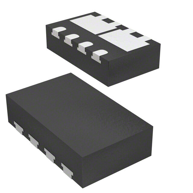
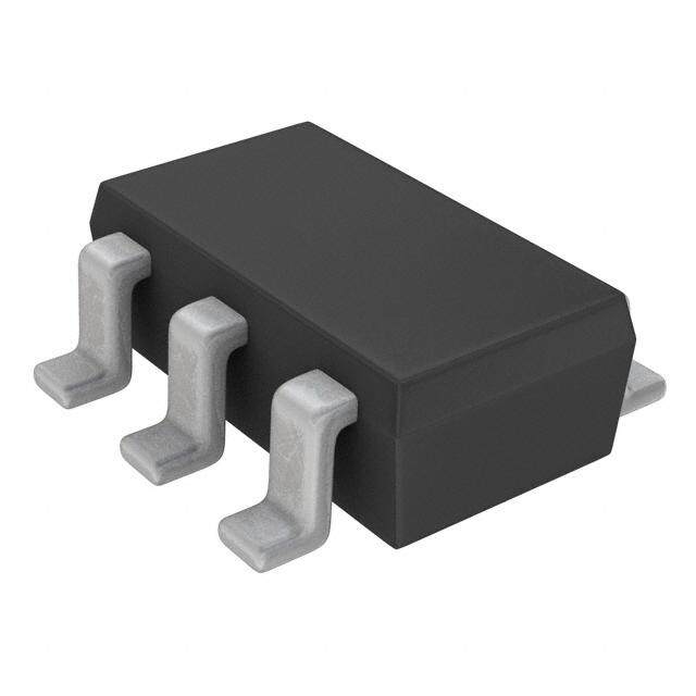
ICGOO电子元器件商城为您提供FDG1024NZ由Fairchild Semiconductor设计生产,在icgoo商城现货销售,并且可以通过原厂、代理商等渠道进行代购。 FDG1024NZ价格参考¥2.08-¥2.59。Fairchild SemiconductorFDG1024NZ封装/规格:晶体管 - FET,MOSFET - 阵列, Mosfet Array 2 N-Channel (Dual) 20V 1.2A 300mW Surface Mount SC-88 (SC-70-6)。您可以下载FDG1024NZ参考资料、Datasheet数据手册功能说明书,资料中有FDG1024NZ 详细功能的应用电路图电压和使用方法及教程。
ON Semiconductor的FDG1024NZ是一款P沟道MOSFET阵列器件,内部集成两个独立的P沟道MOSFET,采用1.8V逻辑电平兼容设计,具有低导通电阻和小封装(如SC-70),适用于空间受限的便携式电子产品。

其主要应用场景包括:
1. 电源管理与负载开关:广泛用于智能手机、平板电脑和可穿戴设备中,作为电池供电系统的电源开关,实现对不同功能模块的上电/断电控制,降低待机功耗。
2. 信号切换与电平转换:在低电压数字电路中用于双向电平转换,支持1.8V、2.5V、3.3V等不同电压域之间的信号切换,适用于I2C、GPIO等通信接口。
3. 电池供电设备:因其低静态电流和高效率,在蓝牙耳机、智能手表、传感器模块等电池供电产品中用于延长续航时间。
4. 热插拔保护电路:可用于防止设备在运行中插拔造成的电流冲击,保护后级电路。
5. 便携医疗设备与物联网终端:在小型化、低功耗要求高的场景中,提供可靠的开关控制功能。

FDG1024NZ凭借其小尺寸、低功耗和高可靠性,特别适合高密度、高性能的消费类电子和工业应用中的功率开关需求。
| 参数 | 数值 |
| 产品目录 | |
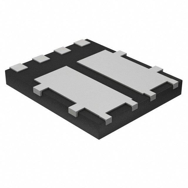
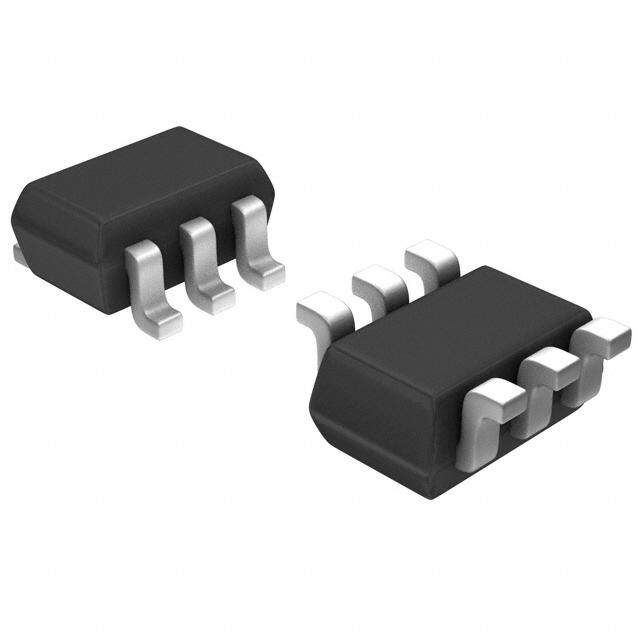
| 描述 | MOSFET N-CH DUAL 20V SC70-6MOSFET Dual PT4 N 20/8V |
| 产品分类 | FET - 阵列分离式半导体 |
| FET功能 | 逻辑电平门 |
| FET类型 | 2 个 N 沟道(双) |
| Id-ContinuousDrainCurrent | 1.2 A |
| Id-连续漏极电流 | 1.2 A |
| 品牌 | Fairchild Semiconductor |
| 产品手册 | |
| 产品图片 |
|
| rohs | 符合RoHS无铅 / 符合限制有害物质指令(RoHS)规范要求 |
| 产品系列 | 晶体管,MOSFET,Fairchild Semiconductor FDG1024NZPowerTrench® |
| 数据手册 | |
| 产品型号 | FDG1024NZ |
| PCN封装 | |
| PCN过时产品 | |
| Pd-PowerDissipation | 0.36 W |
| Pd-功率耗散 | 360 mW |
| RdsOn-Drain-SourceResistance | 321 mOhms |
| RdsOn-漏源导通电阻 | 321 mOhms |
| Vds-Drain-SourceBreakdownVoltage | 20 V |
| Vds-漏源极击穿电压 | 20 V |
| 不同Id时的Vgs(th)(最大值) | 1V @ 250µA |
| 不同Vds时的输入电容(Ciss) | 150pF @ 10V |
| 不同Vgs时的栅极电荷(Qg) | 2.6nC @ 4.5V |
| 不同 Id、Vgs时的 RdsOn(最大值) | 175 毫欧 @ 1.2A,4.5V |
| 产品种类 | MOSFET |
| 供应商器件封装 | SC-70-6 |
| 其它名称 | FDG1024NZFSCT |
| 典型关闭延迟时间 | 11 ns |
| 功率-最大值 | 300mW |
| 包装 | 剪切带 (CT) |
| 单位重量 | 28 mg |
| 商标 | Fairchild Semiconductor |
| 安装类型 | 表面贴装 |
| 安装风格 | SMD/SMT |
| 封装 | Reel |
| 封装/外壳 | 6-TSSOP,SC-88,SOT-363 |
| 封装/箱体 | SC-70-6 |
| 工厂包装数量 | 3000 |
| 晶体管极性 | N-Channel |
| 最大工作温度 | + 150 C |
| 最小工作温度 | - 55 C |
| 标准包装 | 1 |
| 正向跨导-最小值 | 4 S |
| 漏源极电压(Vdss) | 20V |
| 电流-连续漏极(Id)(25°C时) | 1.2A |
| 系列 | FDG1024NZ |
| 配置 | Dual |


- 商务部:美国ITC正式对集成电路等产品启动337调查
- 曝三星4nm工艺存在良率问题 高通将骁龙8 Gen1或转产台积电
- 太阳诱电将投资9.5亿元在常州建新厂生产MLCC 预计2023年完工
- 英特尔发布欧洲新工厂建设计划 深化IDM 2.0 战略
- 台积电先进制程称霸业界 有大客户加持明年业绩稳了
- 达到5530亿美元!SIA预计今年全球半导体销售额将创下新高
- 英特尔拟将自动驾驶子公司Mobileye上市 估值或超500亿美元
- 三星加码芯片和SET,合并消费电子和移动部门,撤换高东真等 CEO
- 三星电子宣布重大人事变动 还合并消费电子和移动部门
- 海关总署:前11个月进口集成电路产品价值2.52万亿元 增长14.8%


PDF Datasheet 数据手册内容提取
Is Now Part of To learn more about ON Semiconductor, please visit our website at www.onsemi.com Please note: As part of the Fairchild Semiconductor integration, some of the Fairchild orderable part numbers will need to change in order to meet ON Semiconductor’s system requirements. Since the ON Semiconductor product management systems do not have the ability to manage part nomenclature that utilizes an underscore (_), the underscore (_) in the Fairchild part numbers will be changed to a dash (-). This document may contain device numbers with an underscore (_). Please check the ON Semiconductor website to verify the updated device numbers. The most current and up-to-date ordering information can be found at www.onsemi.com. Please email any questions regarding the system integration to Fairchild_questions@onsemi.com. ON Semiconductor and the ON Semiconductor logo are trademarks of Semiconductor Components Industries, LLC dba ON Semiconductor or its subsidiaries in the United States and/or other countries. ON Semiconductor owns the rights to a number of patents, trademarks, copyrights, trade secrets, and other intellectual property. A listing of ON Semiconductor’s product/patent coverage may be accessed at www.onsemi.com/site/pdf/Patent-Marking.pdf. ON Semiconductor reserves the right to make changes without further notice to any products herein. ON Semiconductor makes no warranty, representation or guarantee regarding the suitability of its products for any particular purpose, nor does ON Semiconductor assume any liability arising out of the application or use of any product or circuit, and specifically disclaims any and all liability, including without limitation special, consequential or incidental damages. Buyer is responsible for its products and applications using ON Semiconductor products, including compliance with all laws, regulations and safety requirements or standards, regardless of any support or applications information provided by ON Semiconductor. “Typical” parameters which may be provided in ON Semiconductor data sheets and/or specifications can and do vary in different applications and actual performance may vary over time. All operating parameters, including “Typicals” must be validated for each customer application by customer’s technical experts. ON Semiconductor does not convey any license under its patent rights nor the rights of others. ON Semiconductor products are not designed, intended, or authorized for use as a critical component in life support systems or any FDA Class 3 medical devices or medical devices with a same or similar classification in a foreign jurisdiction or any devices intended for implantation in the human body. Should Buyer purchase or use ON Semiconductor products for any such unintended or unauthorized application, Buyer shall indemnify and hold ON Semiconductor and its officers, employees, subsidiaries, affiliates, and distributors harmless against all claims, costs, damages, and expenses, and reasonable attorney fees arising out of, directly or indirectly, any claim of personal injury or death associated with such unintended or unauthorized use, even if such claim alleges that ON Semiconductor was negligent regarding the design or manufacture of the part. ON Semiconductor is an Equal Opportunity/Affirmative Action Employer. This literature is subject to all applicable copyright laws and is not for resale in any manner.
F D G 1 0 June 2010 24 FDG1024NZ N Z ® D Dual N-Channel PowerTrench MOSFET u a 20 V, 1.2 A, 175 mΩ l N Features General Description - C h (cid:132) Max r = 175 mΩ at V = 4.5 V, I = 1.2 A This dual N-Channel logic level enhancement mode field effect DS(on) GS D a transistors are produced using Fairchild’s proprietary, high cell n (cid:132) Max rDS(on) = 215 mΩ at VGS = 2.5 V, ID = 1.0 A density, DMOS technology. This very high density process is n e (cid:132) Max rDS(on) = 270 mΩ at VGS = 1.8 V, ID = 0.9 A especially tailored to minimize on-state resistance. This device l has been designed especially for low voltage applications as a P (cid:132) Max rDS(on) = 389 mΩ at VGS = 1.5 V, ID = 0.8 A replacement for bipolar digital transistors and small signal o w (cid:132) HBM ESD protection level >2 kV (Note 3) MOSFETs. Since bias resistors are not required, this dual digital e FET can replace several different digital transistors, with r (cid:132) Very low level gate drive requirements allowing operation in different bias resistor values. T 1.5 V circuits (V < 1 V) r GS(th) e n (cid:132) Very small package outline SC70-6 c h (cid:132) RoHS Compliant ® M O S F E T S2 G2 D1 S1 1 6 D1 G1 2 5 G2 D2 G1 D2 3 4 S2 S1 SC70-6 MOSFET Maximum Ratings TA = 25 °C unless otherwise noted Symbol Parameter Ratings Units V Drain to Source Voltage 20 V DS V Gate to Source Voltage ±8 V GS -Continuous T = 25°C (Note 1a) 1.2 I A A D -Pulsed 6 Power Dissipation T = 25°C (Note 1a) 0.36 P A W D Power Dissipation T = 25°C (Note 1b) 0.30 A T , T Operating and Storage Junction Temperature Range -55 to +150 °C J STG Thermal Characteristics R Thermal Resistance, Junction to Ambient (Note 1a) 350 θJA °C/W R Thermal Resistance, Junction to Ambient (Note 1b) 415 θJA Package Marking and Ordering Information Device Marking Device Package Reel Size Tape Width Quantity .4N FDG1024NZ SC70-6 7 ” 8 mm 3000 units ©2010 Fairchild Semiconductor Corporation 1 www.fairchildsemi.com FDG1024NZ Rev.C
Electrical Characteristics F T = 25 °C unless otherwise noted J D G Symbol Parameter Test Conditions Min Typ Max Units 1 0 Off Characteristics 2 4 BVDSS Drain to Source Breakdown Voltage ID = 250 µA, VGS = 0 V 20 V N ∆BV Breakdown Voltage Temperature Z ∆TDSS Coefficient ID = 250 µA, referenced to 25 °C 14 mV/°C D J u IDSS Zero Gate Voltage Drain Current VDS = 16 V, VGS = 0 V 1 µA a l I Gate to Source Leakage Current V = ±8 V, V = 0 V ±10 µA GSS GS DS N - On Characteristics C h V Gate to Source Threshold Voltage V = V , I = 250 µA 0.4 0.8 1.0 V a GS(th) GS DS D n ∆V Gate to Source Threshold Voltage n ∆TGS(th) Temperature Coefficient ID = 250 µA, referenced to 25 °C -3 mV/°C e J l V = 4.5 V, I = 1.2 A 160 175 P GS D o VGS = 2.5 V, ID = 1.0 A 185 215 w V = 1.8 V, I = 0.9 A 232 270 e rDS(on) Static Drain to Source On Resistance VGGSS = 1.5 V, IDD = 0.8 A 321 389 mΩ r T VGS = 4.5 V, ID = 1.2 A, 220 259 re T =125 °C n J c gFS Forward Transconductance VDD = 5 V, ID = 1.2 A 4 S h ® Dynamic Characteristics M O C Input Capacitance 115 150 pF iss V = 10 V, V = 0 V, S Coss Output Capacitance f =D S1 MHz GS 25 35 pF F E C Reverse Transfer Capacitance 20 25 pF rss T R Gate Resistance 4.6 Ω g Switching Characteristics t Turn-On Delay Time 3.7 10 ns d(on) tr Rise Time VDD = 10 V, ID = 1.2 A, 1.7 10 ns td(off) Turn-Off Delay Time VGS = 4.5 V, RGEN = 6 Ω 11 19 ns t Fall Time 1.5 10 ns f Q Total Gate Charge 1.8 2.6 nC g V = 4.5 V, V = 10 V, Q Gate to Source Charge GS DD 0.3 nC gs I = 1.2 A D Q Gate to Drain “Miller” Charge 0.4 nC gd Drain-Source Diode Characteristics I Maximum Continuous Drain-Source Diode Forward Current 0.3 A S V Source to Drain Diode Forward Voltage V = 0 V, I = 0.3 A (Note 2) 0.7 1.2 V SD GS S t Reverse Recovery Time 10 20 ns rr I = 1.2 A, di/dt = 100 A/µs Q Reverse Recovery Charge F 1.9 10 nC rr NOTES: 1. RθJA is determined with the device mounted on a 1 in2 pad 2 oz copper pad on a 1.5 x 1.5 in. board of FR-4 material. RθJC is guaranteed by design while RθJA is determined by the user's board design. a. 350 °C/W when mounted b. 415 °C/W when mounted on a on a 1 in2 pad of 2 oz copper. minimum pad of 2 oz copper. 2. Pulse Test: Pulse Width < 300 µs, Duty cycle < 2.0%. 3: The diode connected between the gate and source serves only as protection against ESD. No gate overvoltage rating is implied. ©2010 Fairchild Semiconductor Corporation 2 www.fairchildsemi.com FDG1024NZ Rev.C
F D T ypical Characteristics T = 25 °C unless otherwise noted G J 1 0 2 6 2.5 4 VGS = 4.5 V CE N NT (A) 45 VGS = 3.5 V VGS = 2.5 V DRESISTAN2.0 VGS = 1.5 V VGS = 1.8 V VGS = 2.5 V Z Dua N CURRE 3 PDUULTSYE C DYUCRLEA T=I O0.N5 %= 8M0A µXs RMALIZE RCE ON-1.5 VGS = 3.5 V l N-C , IDRAID 12 VVGGSS == 11..85 VV NORAIN TO SOU1.0 PDUULTSYE C DYUCRLEA T=I O0.N5 %= 8M0A µXs VGS = 4.5 V hannel 0 D0.5 P 0 0.4 0.8 1.2 1.6 2.0 0 1 2 3 4 5 6 o w VDS, DRAIN TO SO URCE VOLTAGE (V) ID, DRAIN CURR ENT (A) e r Figure 1. On-Region Characteristics Figure 2. Normalized On-Resistance T vs Drain Current and Gate Voltage r e n c 1.6 600 h E ID = 1.2 A PULSE DURATION = 80 µs ® ANC 1.4 VGS = 4.5 V )mΩ 500 DUTY CYCLE = 0.5% MAX M NORMALIZED AIN TO SOURCE ON-RESIST 011...802 rDRAIN TO ,DS(on)(SOURCE ON-RESISTANCE 123400000000 TITDJJ = == 112.2525 oA CoC OSFET R D 0.6 0 -75 -50 -25 0 25 50 75 100 125 150 1.0 1.5 2.0 2.5 3.0 3.5 4.0 4.5 TJ, JUNCTION TEM PERATURE (oC) VGS, GATE TO SOURCE VOLTAGE (V) Figure 3. Normalized On- Resistance Figure 4. On-Resistance vs Gate to vs Junction Temperature Source Voltage 6 10 PULSE DURATION = 80 µs A) VGS = 0 V 5 DUTY CYCLE = 0.5% MAX NT ( NT (A) 4 VDS = 5 V CURRE 1 TJ = 125 oC E N AIN CURR 23 TJ = 25 oC RSE DRAI 0.1 TJ = 25 oC R E I, DD 1 TJ = 125 oC TJ = -55 oC I, REVS TJ = -55 oC 0 0.01 0 1 2 3 4 0.2 0.4 0.6 0.8 1.0 1.2 1.4 VGS, GATE TO SOU RCE VOLTAGE (V) VSD, BODY DIODE FOR WARD VOLTAGE (V) Figure 5. Transfer Characteristics Figure 6. Source to Drain Diode Forward Voltage vs Source Current ©2010 Fairchild Semiconductor Corporation 3 www.fairchildsemi.com FDG1024NZ Rev.C
F D Typical Characteristics T = 25 °C unless otherwise noted G J 1 0 5 300 2 4 V) ID = 1.2 A N GE ( 4 Ciss Z OLTA VDD = 5 V pF) 100 Du CE V 3 VDD = 10 V NCE ( al N TO SOUR 2 VDD = 15 V APACITA Coss -Cha E C n GAT 1 10 f = 1 MHz Crss ne V, GS 0 5 VGS = 0 V l P 0 0.5 1.0 1.5 2.0 2.5 0.1 1 10 20 o w Qg, GATE CHARGE (nC) VDS, DRAIN TO SOU RCE VOLTAGE (V) e r Figure 7. Gate Charge Characteristics Figure 8. Capacitance vs Drain T to Source Voltage r e n c 10 105 h RRENT (A) 1 TLIHMISIT AERDE BAY I SrD S(on) 01. 1m mss CURRENT A()µ 103 VGS = 0 V MOSFE® N CU 10 ms AGE 10 TJ = 125 oC T RAI 0.1 SINGLE PULSE EAK I, DD TRJθ J=A M= A4X1 5R oACT/WED 100 ms ATE L 10-1 TJ = 25 oC TA = 25 oC 1D Cs , Gg 0.01 I 10-3 0.01 0.1 1 10 100 0 2 4 6 8 10 12 14 VDS, DRAIN to SOU RCE VOLTAGE (V) VGS, GATE TO SOURCE VOLTAGE (V) Figure 9. Forward Bias Safe Figure 10. Gate Leakage Current vs Gate to Source Operating Area Voltage 100 W) VGS = 4.5 V R ( E W O T P 10 SINGLE PULSE EN RθJA = 415 oC/W NSI TA = 25 oC A R T K A 1 E P , )K P P( 0.1 10-4 10-3 10-2 10-1 1 10 100 1000 t, PULSE WIDTH (sec) Figure 11. Single Pulse Maximum Power Dissipation ©2010 Fairchild Semiconductor Corporation 4 www.fairchildsemi.com FDG1024NZ Rev.C
F Typical Characteristics D T = 25 °C unless otherwise noted J G 1 0 2 4 2 N 1 DUTY CYCLE-DESCENDING ORDER Z D L u ERMAZJAθ 0.1 D = 00..25 al N RMALIZED TH IMPEDANCE, 0.01 0000....1000521 PDM t1t2 -Chann NO SINGLE PULSE NOTES: e RθJA = 415 oC/W DPEUATKY FTAJ C= TPODRM: x D Z =θJ tA1 /xt2 RθJA + TA l P o 0.001 w 10-4 10-3 10-2 10-1 1 10 100 1000 e r t, RECTANGULAR PULSE DURATION (sec) T r Figure 12. Transient Thermal Response Curve e n c h ® M O S F E T ©2010 Fairchild Semiconductor Corporation 5 www.fairchildsemi.com FDG1024NZ Rev.C
F D Dimensional Outline and Pad Layout G 1 0 2 4 N Z D u a l N - C h a n n e l P o w e r T r e n c h ® M O S F E T ©2010 Fairchild Semiconductor Corporation 6 www.fairchildsemi.com FDG1024NZ Rev.C
F D G 1 0 2 4 N TRADEMARKS Z The following includes registered and unregistered trademarks and service marks, owned by Fairchild Semiconductor and/or its global subsidiaries, and is not D intended to be an exhaustive list of all such trademarks. u AccuPower™ F-PFS™ Power-SPM™ ®* a ABuuitlod- Sit PNMo™w™ FGRloFbEaTl P® ower ResourceSM PPoowweerrTXrSe™nc h® The Power Franchise® l N - CorePLUS™ Green FPS™ Programmable Active Droop™ C CorePOWER™ Green FPS™ e-Series™ QFET® h CROSSVOLT™ Gmax™ QS™ TinyBoost™ a CTL™ GTO™ Quiet Series™ TinyBuck™ n Current Transfer Logic™ IntelliMAX™ RapidConfigure™ TinyCalc™ n DEDcuEoaUSl XCPPoAEoREl™KD® ® IMMSeIOCgPRaLBOAuCNcOkA™UR P™L ER™ SSaigvni™nag lW oiusre w™o rld, 1mW/W/kW at a time™ TTTiiInnNyyYPLOoogPwiTce®Or™ ™ el Po EfficientMax™ MicroFET™ SmartMax™ TinyPWM™ w FEaSiBrcCh®™i ld ® MMMiiilcclerroorDPPraaivkke2™™™ SSSPMTEMAA®R LTT SHT™A RT™ TTTiRrniFUyaWEuCilrt eUD™Re RteEctN™T ™* er Tr FFFFFFaAAAEasiCSCTrtcBvTTThC®e ®iQl noducr eShie™e™tm Siecroiensd™uc tor® OMMOOPPpootttTToiiooOOH®nnPL iM-TSOL™aPAGxM N™IC™A ®R ® SSSSSSuuuuyunpppppeceeererFrrrSFSSMEOEOOTOTT™TTS™™™™ ™- 3-- 68 UUUμSHlntreiCFar ED®F TeRs™F™ E T™ enchM® FlashWriter®* Sync-Lock™ VCX™ O PDP SPM™ VisualMax™ S FPS™ XS™ F * Trademarks of System General Corporation, used under license by Fairchild Semiconductor. E T DISCLAIMER FAIRCHILD SEMICONDUCTOR RESERVES THE RIGHT TO MAKE CHANGES WITHOUT FURTHER NOTICE TO ANY PRODUCTS HEREIN TO IMPROVE RELIABILITY, FUNCTION, OR DESIGN. FAIRCHILD DOES NOT ASSUME ANY LIABILITY ARISING OUT OF THE APPLICATION OR USE OF ANY PRODUCT OR CIRCUIT DESCRIBED HEREIN; NEITHER DOES IT CONVEY ANY LICENSE UNDER ITS PATENT RIGHTS, NOR THE RIGHTS OF OTHERS. THESE SPECIFICATIONS DO NOT EXPAND THE TERMS OF FAIRCHILD’S WORLDWIDE TERMS AND CONDITIONS, SPECIFICALLY THE WARRANTY THEREIN, WHICH COVERS THESE PRODUCTS. LIFE SUPPORT POLICY FAIRCHILD’S PRODUCTS ARE NOT AUTHORIZED FOR USE AS CRITICAL COMPONENTS IN LIFE SUPPORT DEVICES OR SYSTEMS WITHOUT THE EXPRESS WRITTEN APPROVAL OF FAIRCHILD SEMICONDUCTOR CORPORATION. As used herein: 1. Life support devices or systems are devices or systems which, (a) are 2. A critical component in any component of a life support, device, or intended for surgical implant into the body or (b) support or sustain life, system whose failure to perform can be reasonably expected to and (c) whose failure to perform when properly used in accordance cause the failure of the life support device or system, or to affect its with instructions for use provided in the labeling, can be reasonably safety or effectiveness. expected to result in a significant injury of the user. ANTI-COUNTERFEITING POLICY Fairchild Semiconductor Corporation's Anti-Counterfeiting Policy. Fairchild's Anti-Counterfeiting Policy is also stated on our external website, www.fairchildsemi.com, under Sales Support. Counterfeiting of semiconductor parts is a growing problem in the industry. All manufacturers of semiconductor products are experiencing counterfeiting of their parts. Customers who inadvertently purchase counterfeit parts experience many problems such as loss of brand reputation, substandard performance, failed applications, and increased cost of production and manufacturing delays. Fairchild is taking strong measures to protect ourselves and our customers from the proliferation of counterfeit parts. Fairchild strongly encourages customers to purchase Fairchild parts either directly from Fairchild or from Authorized Fairchild Distributors who are listed by country on our web page cited above. Products customers buy either from Fairchild directly or from Authorized Fairchild Distributors are genuine parts, have full traceability, meet Fairchild's quality standards for handling and storage and provide access to Fairchild's full range of up-to-date technical and product information. Fairchild and our Authorized Distributors will stand behind all warranties and will appropriately address any warranty issues that may arise. Fairchild will not provide any warranty coverage or other assistance for parts bought from Unauthorized Sources. Fairchild is committed to combat this global problem and encourage our customers to do their part in stopping this practice by buying direct or from authorized distributors. PRODUCT STATUS DEFINITIONS Definition of Terms Datasheet Identification Product Status Definition Datasheet contains the design specifications for product development. Specifications may change in Advance Information Formative / In Design any manner without notice. Datasheet contains preliminary data; supplementary data will be published at a later date. Fairchild Preliminary First Production Semiconductor reserves the right to make changes at any time without notice to improve design. Datasheet contains final specifications. Fairchild Semiconductor reserves the right to make changes No Identification Needed Full Production at any time without notice to improve the design. Datasheet contains specifications on a product that is discontinued by Fairchild Semiconductor. Obsolete Not In Production The datasheet is for reference information only. Rev. I48 ©2010 Fairchild Semiconductor Corporation 7 www.fairchildsemi.com FDG1024NZ Rev.C
ON Semiconductor and are trademarks of Semiconductor Components Industries, LLC dba ON Semiconductor or its subsidiaries in the United States and/or other countries. ON Semiconductor owns the rights to a number of patents, trademarks, copyrights, trade secrets, and other intellectual property. A listing of ON Semiconductor’s product/patent coverage may be accessed at www.onsemi.com/site/pdf/Patent−Marking.pdf. ON Semiconductor reserves the right to make changes without further notice to any products herein. ON Semiconductor makes no warranty, representation or guarantee regarding the suitability of its products for any particular purpose, nor does ON Semiconductor assume any liability arising out of the application or use of any product or circuit, and specifically disclaims any and all liability, including without limitation special, consequential or incidental damages. Buyer is responsible for its products and applications using ON Semiconductor products, including compliance with all laws, regulations and safety requirements or standards, regardless of any support or applications information provided by ON Semiconductor. “Typical” parameters which may be provided in ON Semiconductor data sheets and/or specifications can and do vary in different applications and actual performance may vary over time. All operating parameters, including “Typicals” must be validated for each customer application by customer’s technical experts. ON Semiconductor does not convey any license under its patent rights nor the rights of others. ON Semiconductor products are not designed, intended, or authorized for use as a critical component in life support systems or any FDA Class 3 medical devices or medical devices with a same or similar classification in a foreign jurisdiction or any devices intended for implantation in the human body. Should Buyer purchase or use ON Semiconductor products for any such unintended or unauthorized application, Buyer shall indemnify and hold ON Semiconductor and its officers, employees, subsidiaries, affiliates, and distributors harmless against all claims, costs, damages, and expenses, and reasonable attorney fees arising out of, directly or indirectly, any claim of personal injury or death associated with such unintended or unauthorized use, even if such claim alleges that ON Semiconductor was negligent regarding the design or manufacture of the part. ON Semiconductor is an Equal Opportunity/Affirmative Action Employer. This literature is subject to all applicable copyright laws and is not for resale in any manner. PUBLICATION ORDERING INFORMATION LITERATURE FULFILLMENT: N. American Technical Support: 800−282−9855 Toll Free ON Semiconductor Website: www.onsemi.com Literature Distribution Center for ON Semiconductor USA/Canada 19521 E. 32nd Pkwy, Aurora, Colorado 80011 USA Europe, Middle East and Africa Technical Support: Order Literature: http://www.onsemi.com/orderlit Phone: 303−675−2175 or 800−344−3860 Toll Free USA/Canada Phone: 421 33 790 2910 Fax: 303−675−2176 or 800−344−3867 Toll Free USA/Canada Japan Customer Focus Center For additional information, please contact your local Email: orderlit@onsemi.com Phone: 81−3−5817−1050 Sales Representative © Semiconductor Components Industries, LLC www.onsemi.com www.onsemi.com 1
Mouser Electronics Authorized Distributor Click to View Pricing, Inventory, Delivery & Lifecycle Information: O N Semiconductor: FDG1024NZ