ICGOO在线商城 > 分立半导体产品 > 晶体管 - FET,MOSFET - 射频 > PD85004
 Datasheet下载
- 型号: PD85004
- 制造商: STMicroelectronics
- 库位|库存: xxxx|xxxx
- 要求:
| 数量阶梯 | 香港交货 | 国内含税 |
| +xxxx | $xxxx | ¥xxxx |
查看当月历史价格
查看今年历史价格
PD85004产品简介:
ICGOO电子元器件商城为您提供PD85004由STMicroelectronics设计生产,在icgoo商城现货销售,并且可以通过原厂、代理商等渠道进行代购。 PD85004价格参考。STMicroelectronicsPD85004封装/规格:晶体管 - FET,MOSFET - 射频, 射频 Mosfet LDMOS 13.6V 50mA 870MHz 17dB 4W SOT-89。您可以下载PD85004参考资料、Datasheet数据手册功能说明书,资料中有PD85004 详细功能的应用电路图电压和使用方法及教程。
STMicroelectronics的PD85004是一款射频MOSFET(金属氧化物半导体场效应晶体管),属于射频功率晶体管类别,广泛应用于需要高效、高频率性能的无线通信系统中。该器件基于先进的LDMOS(横向扩散金属氧化物半导体)技术,具备优良的功率增益、效率和热稳定性,适合在高频段下工作。

PD85004主要适用于工业、科学和医疗(ISM)频段,以及UHF频段的射频放大应用。典型应用场景包括:射频能量系统(如感应加热、等离子发生)、小型广播发射设备(如调频广播发射机)、无线基础设施中的射频功率放大器模块,以及各类工业射频源设备。此外,由于其良好的线性度和可靠性,也常用于驱动级或末级射频功率放大电路。

该器件通常工作在数百MHz的频率范围内,支持较高的输出功率,同时保持较低的功耗和失真,有助于提升系统整体能效。得益于STMicroelectronics对制造工艺和封装技术的优化,PD85004具备良好的散热性能和长期运行稳定性,适用于紧凑型、高密度的射频设计环境。

综上所述,PD85004适用于对效率、稳定性和集成度有较高要求的中等功率射频放大场景,特别适合工业与通信领域的射频能量和信号传输应用。
| 参数 | 数值 |
| 产品目录 | |
| 描述 | TRANS RF POWER LDMOST射频MOSFET晶体管 RF PWR TRANSISTOR |
| 产品分类 | RF FET分离式半导体 |
| Id-ContinuousDrainCurrent | 2 A |
| Id-连续漏极电流 | 2 A |
| 品牌 | STMicroelectronics |
| 产品手册 | |
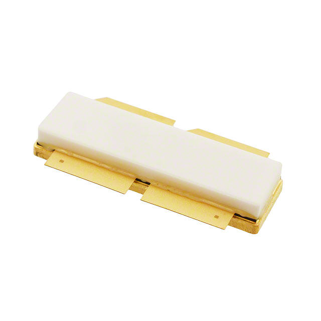
| 产品图片 |
|
| rohs | 符合RoHS无铅 / 符合限制有害物质指令(RoHS)规范要求 |
| 产品系列 | 晶体管,晶体管射频,射频MOSFET晶体管,STMicroelectronics PD85004- |
| 数据手册 | |
| 产品型号 | PD85004 |
| Pd-PowerDissipation | 6 W |
| Pd-功率耗散 | 6 W |
| Vds-Drain-SourceBreakdownVoltage | 40 V |
| Vds-漏源极击穿电压 | 40 V |
| Vgs-Gate-SourceBreakdownVoltage | 15 V |
| Vgs-栅源极击穿电压 | 15 V |
| 产品目录页面 | |
| 产品种类 | 射频MOSFET晶体管 |
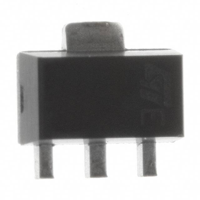
| 供应商器件封装 | SOT-89 |
| 其它名称 | 497-8291 |
| 其它有关文件 | http://www.st.com/web/catalog/sense_power/FM1987/CL1989/SC1821/PF199440?referrer=70071840 |
| 功率-输出 | 4W |
| 功率耗散 | 6 W |
| 包装 | 带卷 (TR) |
| 商标 | STMicroelectronics |
| 噪声系数 | - |
| 增益 | 17dB |
| 安装风格 | SMD/SMT |
| 封装 | Reel |
| 封装/外壳 | TO-243AA |
| 封装/箱体 | SOT-89 |
| 工厂包装数量 | 2500 |
| 技术 | LDMOS |
| 晶体管极性 | N-Channel |
| 晶体管类型 | LDMOS |
| 最大工作温度 | + 150 C |
| 最小工作温度 | - 65 C |
| 标准包装 | 2,500 |
| 汲极/源极击穿电压 | 40 V |
| 漏极连续电流 | 2 A |
| 特色产品 | http://www.digikey.com/cn/zh/ph/ST/pd8.html |
| 电压-测试 | 13.6V |
| 电压-额定 | 40V |
| 电流-测试 | 50mA |
| 系列 | PD85004 |
| 输出功率 | 4 W |
| 配置 | Single |
| 闸/源击穿电压 | 15 V |
| 频率 | 870MHz |
| 额定电流 | 2A |


.jpg)


- 商务部:美国ITC正式对集成电路等产品启动337调查
- 曝三星4nm工艺存在良率问题 高通将骁龙8 Gen1或转产台积电
- 太阳诱电将投资9.5亿元在常州建新厂生产MLCC 预计2023年完工
- 英特尔发布欧洲新工厂建设计划 深化IDM 2.0 战略
- 台积电先进制程称霸业界 有大客户加持明年业绩稳了
- 达到5530亿美元!SIA预计今年全球半导体销售额将创下新高
- 英特尔拟将自动驾驶子公司Mobileye上市 估值或超500亿美元
- 三星加码芯片和SET,合并消费电子和移动部门,撤换高东真等 CEO
- 三星电子宣布重大人事变动 还合并消费电子和移动部门
- 海关总署:前11个月进口集成电路产品价值2.52万亿元 增长14.8%


PDF Datasheet 数据手册内容提取
PD85004 RF power transistor the LdmoST plastic family Features ■ Excellent thermal stability ■ Common source configuration ■ Broadband performances P = 4 W with 17 dB gain @ 870 MHz OUT ■ Plastic package ■ ESD protection SOT-89 ■ Supplied in tape and reel ■ In compliance with the 2002/95/EC european Figure 1. Pin connection directive Description Source The PD85004 is a common source N-channel, enhancement-mode lateral field-effect RF power transistor. It is designed for high gain, broad band commercial and industrial applications. It operates at 13.6 V in common source mode at frequencies of up to 1 GHz. PD85004’s superior gain and efficiency makes it an ideal solution for mobile radio. Source Gate Drain Table 1. Device summary Order code Marking Package Packaging PD85004 8504 SOT-89 Tape and reel August 2008 Rev 2 1/18 www.st.com 18
Contents PD85004 Contents 1 Electrical data . . . . . . . . . . . . . . . . . . . . . . . . . . . . . . . . . . . . . . . . . . . . . . 3 1.1 Maximum ratings . . . . . . . . . . . . . . . . . . . . . . . . . . . . . . . . . . . . . . . . . . . . 3 1.2 Thermal data . . . . . . . . . . . . . . . . . . . . . . . . . . . . . . . . . . . . . . . . . . . . . . . 3 2 Electrical characteristics . . . . . . . . . . . . . . . . . . . . . . . . . . . . . . . . . . . . . 4 2.1 Static . . . . . . . . . . . . . . . . . . . . . . . . . . . . . . . . . . . . . . . . . . . . . . . . . . . . . 4 2.2 Dynamic . . . . . . . . . . . . . . . . . . . . . . . . . . . . . . . . . . . . . . . . . . . . . . . . . . . 4 2.3 ESD protection characteristics . . . . . . . . . . . . . . . . . . . . . . . . . . . . . . . . . . 4 2.4 Moisture sensitivity level . . . . . . . . . . . . . . . . . . . . . . . . . . . . . . . . . . . . . . . 4 3 Impedances . . . . . . . . . . . . . . . . . . . . . . . . . . . . . . . . . . . . . . . . . . . . . . . . 5 4 DC curves . . . . . . . . . . . . . . . . . . . . . . . . . . . . . . . . . . . . . . . . . . . . . . . . . 6 5 RF curves . . . . . . . . . . . . . . . . . . . . . . . . . . . . . . . . . . . . . . . . . . . . . . . . . . 7 6 Schematic and BOM . . . . . . . . . . . . . . . . . . . . . . . . . . . . . . . . . . . . . . . . . 9 7 Demonstration board photo . . . . . . . . . . . . . . . . . . . . . . . . . . . . . . . . . . 11 8 Package mechanical data . . . . . . . . . . . . . . . . . . . . . . . . . . . . . . . . . . . . 12 8.1 Thermal pad and via design . . . . . . . . . . . . . . . . . . . . . . . . . . . . . . . . . . . 14 8.2 Soldering profile . . . . . . . . . . . . . . . . . . . . . . . . . . . . . . . . . . . . . . . . . . . . 15 9 Revision history . . . . . . . . . . . . . . . . . . . . . . . . . . . . . . . . . . . . . . . . . . . 17 2/18
PD85004 Electrical data 1 Electrical data 1.1 Maximum ratings Table 2. Absolute maximum ratings (T = 25 °C) CASE Symbol Parameter Value Unit V Drain-source voltage 40 V (BR)DSS V Gate-source voltage -0.5 to +15 V GS I Drain current 2 A D P Power dissipation 6 W DISS T Max. operating junction temperature 150 °C J T Storage temperature -65 to +150 °C STG 1.2 Thermal data Table 3. Thermal data Symbol Parameter Value Unit R Junction - case thermal resistance 21 °C/W thJC 3/18
Electrical characteristics PD85004 2 Electrical characteristics T = +25 oC CASE 2.1 Static T able 4. Static Symbol Test conditions Min Typ Max Unit I V = 0 V V = 25 V 1 μA DSS GS DS I V = 5 V V = 0 V 1 μA GSS GS DS V V = 13.6 V I = 50 mA 3.9 V GS(Q) DS D V V = 10 V I = 0.25 A 0.27 V DS(ON) GS D C V = 0 V V = 13.6 V f = 1 MHz 16 pF ISS GS DS C V = 0 V V = 13.6 V f = 1 MHz 14 pF OSS GS DS C V = 0 V V = 13.6 V f = 1 MHz 1.1 pF RSS GS DS 2.2 Dynamic T able 5. Dynamic Symbol Test conditions Min Typ Max Unit P V = 13.6 V, I = 50 mA, P = 0.1 W, f = 870 MHz 4 5 W OUT DD DQ IN G V = 13.6 V, I = 50 mA, P = 4 W, f = 870 MHz 15 17 dB PS DD DQ OUT N V = 13.6 V, I = 50 mA, P = 4 W, f = 870 MHz 60 65 % D DD DQ OUT Load V = 13.6 V, I = 50 mA, P = 4 W, f = 870 MHz DD DQ OUT 20:1 VSWR mismatch All phase angles 2.3 ESD protection characteristics T able 6. ESD protection characteristics Test conditions Class Human body model 2 Machine model M3 2.4 Moisture sensitivity level T able 7. Moisture sensitivity level Test methodology Rating J-STD-020B MSL 3 4/18
PD85004 Impedances 3 Impedances Figure 2. Impedances Table 8. Broadband impedances F(MHz) Z Z GS DL 860 2.46+ j 6.63 8.38+ j 2,83 880 2.59+ j 6.83 8.08+ j 3.46 900 2.63+ j 6.97 7.77 + j 4.10 920 2.57+ j 7.09 7.50+ j 4.77 940 2.42+ j 7.17 7.15+ j 5.37 960 2.27+ j 7.34 6.95+ j 6.07 5/18
DC curves PD85004 4 DC curves Figure 3. DC output characteristics Figure 4. ID vs V GS ID vs Vgs VGS=10V VGS=9V VGS=8V VGS=7V PD84002 VGS=6V VGS=5V VGS=4V Figure 5. Capacitances vs drain voltage 30 25 CRSS COSS CISS F) 20 p e ( citanc 15 pa a C 10 5 0 0 2 4 6 8 10 12 14 16 Vdd (V) 6/18
PD85004 RF curves 5 RF curves Figure 6. O utput power and drain efficiency Figure 7. Gain vs frequency vs frequency 13.6 V / 50 mA 13.6 V / 50 mA / Pin = 19 dBm Gain vs Frequency 6 80 13.6V / 50mA 20 70 19 5 60 18 Pout (W)4 345000Efficiency (%) Gain (dB)111567 Pin=19 dBm 3 Pout Eff 20 14 10 13 12 2 0 860 880 900 920 940 960 860 880 900 920 940 960 Frequency (MHz) Frequency (MHz) Figure 8. Input return loss vs frequency Figure 9. Gain vs output power 13.6 V / 50 mA 13.6 V / 50 mA 13.6V / 50mA 0 20 -2 19 -4 Pin=19 dBm 18 -6 17 B) B) -8 n (d16 RL (d-10 Gai1145 860 MHz 900 MHz 960 MHz I-12 13 -14 12 -16 11 -18 0 1 2 3 4 5 6 7 Pout (W) -20 820 840 860 880 900 920 940 960 980 1000 Frequency (MHz) Figure 10. Drain current vs output power Figure 11. Output power vs input power 13.6 V / 50 mA 13.6 V / 50 mA 0.8 40 0.7 860 MHz 900 MHz 960 MHz 38 Drain current (A)000...456 Output power (dBm)2333380246 860 MHz 900 MHz 960 MHz 0.3 26 0.2 24 28 29 30 31 32 33 34 35 36 37 38 39 40 12 13 14 15 16 17 18 19 20 21 22 23 24 25 Output Power (dBm) Input power (dBm) 7/18
RF curves PD85004 Figure 12. Harmonics vs frequency 13.6 V / 50 mA 0 -10 H2 H3 -20 B) s (d-30 c ni-40 o m ar-50 H -60 -70 -80 860 880 900 920 940 960 Frequency (MHz) 8/18
PD85004 Schematic and BOM 6 Schematic and BOM Figure 13. Schematic Vcc 1 + MSub R3 + 2 - B2 B1 C3 C4 C5 FR4 H=20 mil R2 C1 L1 C2 R1 TL4 TL5 TL6 C7 RFout C11 C12 RFin C6 TL1 TL2 TL3 LDMOS C8 C9 C10 PD85004 9/18
Schematic and BOM PD85004 Table 9. Components part list Component ID Description Value Case size Manufacturer Part code B1 Ferrite bead Panasonic EXCELDRC35C B2 Ferrite bead Panasonic EXCELDRC35C C1, C2 Capacitor 120 pF 0603 Murata GRM39-C0G121J50D500 C3 Capacitor 1 nF 0603 Murata GRM39-X7R102K50C560 C4 Capacitor 10 nF 0603 Murata GRM39-X7R103K50C560 C5 Capacitor 10 uF SMT Panasonic EEVHB1V100P C6, C7 Capacitor 39 pF 0603 Murata GRM39-C0G390J50D500 C8 Capacitor 3.3 pF 0603 Murata GRM39-C0G3R3C50Z500 C9 Capacitor 12 pF 0603 Murata GRM39-C0G120J50D500 C10 Capacitor 22 pF 0603 Murata GRM39-C0G220J50D500 C11 Capacitor 6,8 pF 0603 Murata GRM39-C0G6R8D50Z500 C12 Capacitor 1,5 pF 0603 Murata GRM39-C0G1R5C50Z500 L1 Inductor 12.55 nH Coilcraft 1606-10 R1 Resistor 150 Ω 0603 Tyco electronics R2 Potentiometer 10 KΩ Bourns electronics 3214W-1-103E R3 Resistor 1 K 0603 Tyco electronics 01623440-1 TL1 W= 0.92 mm L = 13.6 mm TL2 W=0.92 mm L = 3.5 mm TL3 Transmission W=0.92 mm L = 4.2 mm TL4 Line W=0.92 mm L = 3.8 mm TL5 W=0.92 mm L = 4.2 mm TL6 W=0.92 mm L = 11.3 mm RF in, RF out SMA-CONN 50 Ω 60 mils JOHNSON 142-0701-801 PD85004 LDMOS STMicroelectronics PD85004 Board FR-4 THk = 0.020" 2 OZ Cu both sides 10/18
PD85004 Demonstration board photo 7 Demonstration board photo Figure 14. Demonstration board photo 11/18
Package mechanical data PD85004 8 Package mechanical data In order to meet environmental requirements, ST offers these devices in ECOPACK® packages. These packages have a lead-free second level interconnect . The category of second level interconnect is marked on the package and on the inner box label, in compliance with JEDEC Standard JESD97. The maximum ratings related to soldering conditions are also marked on the inner box label. ECOPACK is an ST trademark. ECOPACK specifications are available at: www.st.com 12/18
PD85004 Package mechanical data T able 10. SOT-89 mechanical data Dim. mm. Inch Min Typ Max Min Typ Max A 1.4 1.6 55.1 63.0 B 0.44 0.56 17.3 22.0 B1 0.36 0.48 14.2 18.9 C 0.35 0.44 13.8 17.3 C1 0.35 0.44 13.8 17.3 D 4.4 4.6 173.2 181.1 D1 1.62 1.83 63.8 72.0 E 2.29 2.6 90.2 102.4 e 1.42 1.57 55.9 61.8 e1 2.92 3.07 115.0 120.9 H 3.94 4.25 155.1 167.3 L 0.89 1.2 35.0 47.2 Figure 15. Package dimensions 13/18
Package mechanical data PD85004 8.1 Thermal pad and via design Thernal vias are required in the PCB layout to effectively conduct heat away from the package. The via pattern has been designed to address thermal, power dissipation and electrical requirements of the device. The via pattern is based on thru-hole vias with 0.203 mm to 0.330 mm finished hole size on a 0.5 mm to 1.2 mm grid pattern with 0.025 plating on via walls. If micro vias are used in a design, it is suggested that the quantity of vias be increased by a 4:1 ratio to achieve similar results. Figure 16. Pad layout details 14/18
PD85004 Package mechanical data 8.2 Soldering profile Figure17 shows the recommeded solder for devices that have Pb-free terminal plating and where a Pb-free solder is used. Figure 17. Recommended solder profile Figure18 shows the recommeded solder for devices with Pb-free terminal plating used with leaded solder, or for devices with leaded terminal plating used with a leaded solder. Figure 18. Recommended solder profile for leaded devices 15/18
Package mechanical data PD85004 Figure 19. Reel information 16/18
PD85004 Revision history 9 Revision history Table 11. Document revision history Date Revision Changes 05-Dec-2007 1 Initial release. 22-Aug-2008 2 Updated marking in Table1 on page1 17/18
PD85004 Please Read Carefully: Information in this document is provided solely in connection with ST products. STMicroelectronics NV and its subsidiaries (“ST”) reserve the right to make changes, corrections, modifications or improvements, to this document, and the products and services described herein at any time, without notice. All ST products are sold pursuant to ST’s terms and conditions of sale. Purchasers are solely responsible for the choice, selection and use of the ST products and services described herein, and ST assumes no liability whatsoever relating to the choice, selection or use of the ST products and services described herein. No license, express or implied, by estoppel or otherwise, to any intellectual property rights is granted under this document. If any part of this document refers to any third party products or services it shall not be deemed a license grant by ST for the use of such third party products or services, or any intellectual property contained therein or considered as a warranty covering the use in any manner whatsoever of such third party products or services or any intellectual property contained therein. UNLESS OTHERWISE SET FORTH IN ST’S TERMS AND CONDITIONS OF SALE ST DISCLAIMS ANY EXPRESS OR IMPLIED WARRANTY WITH RESPECT TO THE USE AND/OR SALE OF ST PRODUCTS INCLUDING WITHOUT LIMITATION IMPLIED WARRANTIES OF MERCHANTABILITY, FITNESS FOR A PARTICULAR PURPOSE (AND THEIR EQUIVALENTS UNDER THE LAWS OF ANY JURISDICTION), OR INFRINGEMENT OF ANY PATENT, COPYRIGHT OR OTHER INTELLECTUAL PROPERTY RIGHT. UNLESS EXPRESSLY APPROVED IN WRITING BY AN AUTHORIZED ST REPRESENTATIVE, ST PRODUCTS ARE NOT RECOMMENDED, AUTHORIZED OR WARRANTED FOR USE IN MILITARY, AIR CRAFT, SPACE, LIFE SAVING, OR LIFE SUSTAINING APPLICATIONS, NOR IN PRODUCTS OR SYSTEMS WHERE FAILURE OR MALFUNCTION MAY RESULT IN PERSONAL INJURY, DEATH, OR SEVERE PROPERTY OR ENVIRONMENTAL DAMAGE. ST PRODUCTS WHICH ARE NOT SPECIFIED AS "AUTOMOTIVE GRADE" MAY ONLY BE USED IN AUTOMOTIVE APPLICATIONS AT USER’S OWN RISK. Resale of ST products with provisions different from the statements and/or technical features set forth in this document shall immediately void any warranty granted by ST for the ST product or service described herein and shall not create or extend in any manner whatsoever, any liability of ST. ST and the ST logo are trademarks or registered trademarks of ST in various countries. Information in this document supersedes and replaces all information previously supplied. The ST logo is a registered trademark of STMicroelectronics. All other names are the property of their respective owners. © 2008 STMicroelectronics - All rights reserved STMicroelectronics group of companies Australia - Belgium - Brazil - Canada - China - Czech Republic - Finland - France - Germany - Hong Kong - India - Israel - Italy - Japan - Malaysia - Malta - Morocco - Singapore - Spain - Sweden - Switzerland - United Kingdom - United States of America www.st.com 18/18
Mouser Electronics Authorized Distributor Click to View Pricing, Inventory, Delivery & Lifecycle Information: S TMicroelectronics: PD85004