ICGOO在线商城 > 分立半导体产品 > 晶体管 - FET,MOSFET - 阵列 > SIS902DN-T1-GE3

 Datasheet下载
- 型号: SIS902DN-T1-GE3
- 制造商: Vishay
- 库位|库存: xxxx|xxxx
- 要求:
| 数量阶梯 | 香港交货 | 国内含税 |
| +xxxx | $xxxx | ¥xxxx |
查看当月历史价格
查看今年历史价格
SIS902DN-T1-GE3产品简介:
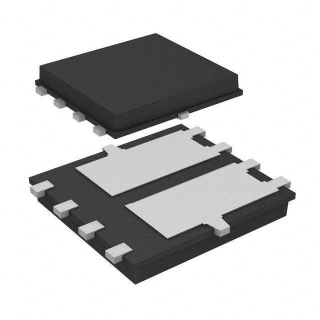
ICGOO电子元器件商城为您提供SIS902DN-T1-GE3由Vishay设计生产,在icgoo商城现货销售,并且可以通过原厂、代理商等渠道进行代购。 SIS902DN-T1-GE3价格参考。VishaySIS902DN-T1-GE3封装/规格:晶体管 - FET,MOSFET - 阵列, Mosfet Array 2 N-Channel (Dual) 75V 4A 15.4W Surface Mount PowerPAK® 1212-8 Dual。您可以下载SIS902DN-T1-GE3参考资料、Datasheet数据手册功能说明书,资料中有SIS902DN-T1-GE3 详细功能的应用电路图电压和使用方法及教程。
Vishay Siliconix的SIS902DN-T1-GE3是一款P沟道MOSFET阵列器件,内置两个独立的P沟道场效应晶体管,采用小型化10引脚PowerPAK® 3.3mm × 3.3mm封装,具有低导通电阻和高功率密度的特点。该器件适用于对空间和能效要求较高的电子系统。

其主要应用场景包括便携式电子产品,如智能手机、平板电脑和可穿戴设备中的电源管理电路,用于负载开关、电池反向保护或电压切换控制。由于具备良好的开关特性和热性能,SIS902DN-T1-GE3也广泛应用于DC-DC转换器中,作为同步整流或高端开关使用,提升电源转换效率。

此外,该器件适用于各类消费类电子和工业控制设备中的信号切换与电源多路控制,例如在主板电源管理模块或多通道电源分配系统中实现低功耗、高可靠性的开关功能。其小型封装特别适合高密度PCB布局,有助于缩小整体产品尺寸。

综上,SIS902DN-T1-GE3凭借其高性能P沟道MOSFET阵列特性,广泛应用于便携设备电源管理、DC-DC转换、负载开关及各类紧凑型电子系统的功率控制场景。
| 参数 | 数值 |
| 产品目录 | |
| 描述 | MOSFET 2N-CH 75V 4A PPAK 1212-8 |
| 产品分类 | FET - 阵列 |
| FET功能 | 标准 |
| FET类型 | 2 个 N 沟道(双) |
| 品牌 | Vishay Siliconix |
| 数据手册 | |
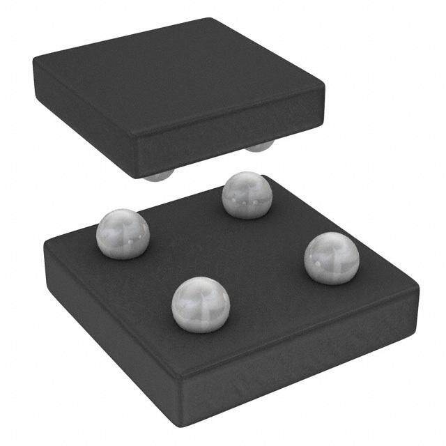
| 产品图片 |
|
| 产品型号 | SIS902DN-T1-GE3 |
| rohs | 无铅 / 符合限制有害物质指令(RoHS)规范要求 |
| 产品系列 | TrenchFET® |
| 不同Id时的Vgs(th)(最大值) | 2.5V @ 250µA |
| 不同Vds时的输入电容(Ciss) | 175pF @ 38V |
| 不同Vgs时的栅极电荷(Qg) | 6nC @ 10V |
| 不同 Id、Vgs时的 RdsOn(最大值) | 186 毫欧 @ 3A,10V |
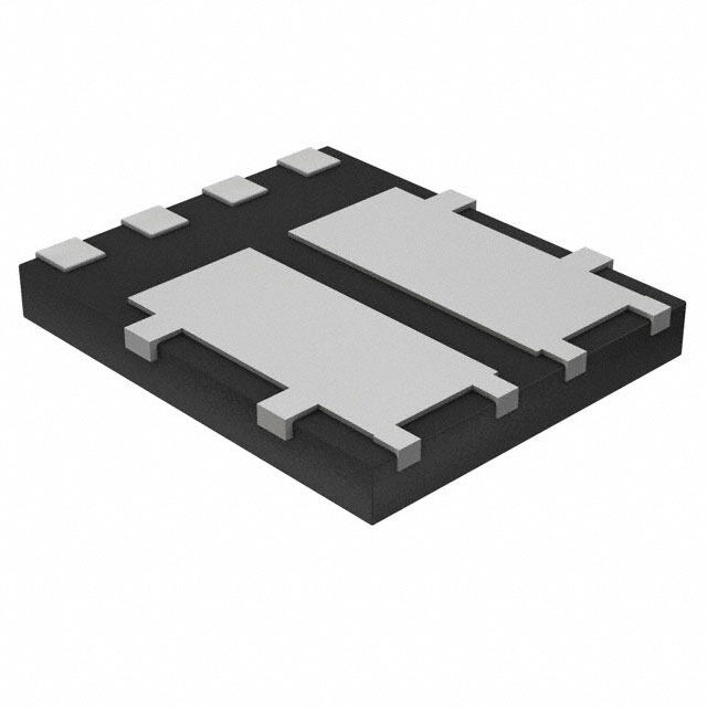
| 供应商器件封装 | PowerPAK® 1212-8 Dual |
| 其它名称 | SIS902DN-T1-GE3DKR |
| 功率-最大值 | 15.4W |
| 包装 | Digi-Reel® |
| 安装类型 | 表面贴装 |
| 封装/外壳 | PowerPAK® 1212-8 双 |
| 标准包装 | 1 |
| 漏源极电压(Vdss) | 75V |
| 电流-连续漏极(Id)(25°C时) | 4A |


PDF Datasheet 数据手册内容提取
SiS902DN Vishay Siliconix Dual N-Channel 75-V (D-S) MOSFET FEATURES PRODUCT SUMMARY • Halogen-free According to IEC 61249-2-21 V (V) R (Ω) I (A) Q (Typ.) DS DS(on) D g Definition 75 0.186 at VGS = 10 V 4e 2.1 nC (cid:129) TrenchFET® Power MOSFET 0.228 at VGS = 4.5 V 4e (cid:129) Low Thermal Resistance PowerPAK® Package with Small Size and Low 1.07 mm Profile (cid:129) 100 % R Tested g (cid:129) 100 % UIS Tested (cid:129) Compliant to RoHS Directive 2002/95/EC APPLICATIONS PowerPAK 1212-8 (cid:129) POL D1 D2 3.30 mm S1 3.30 mm 1 G1 2 S2 3 G2 4 G1 G2 D1 8 D1 7 D2 Bottom View 6 5 D2 S1 S2 Ordering Information: SiS902DN-T1-GE3 (Lead (Pb)-free and Halogen-free) N-Channel MOSFET N-Channel MOSFET ABSOLUTE MAXIMUM RATINGS T = 25 °C, unless otherwise noted A Parameter Symbol Limit Unit Drain-Source Voltage VDS 75 V Gate-Source Voltage VGS ± 20 TC = 25 °C 4e TC = 70 °C 4e Continuous Drain Current (T = 150 °C) I J D TA = 25 °C 3a, b A TA = 70 °C 2.4a, b Pulsed Drain Current IDM 8 Avalanche Current IAS 2 L = 0.1 mH Single-Pulse Avalanche Energy EAS 0.2 mJ TC = 25 °C 15.4 TC = 70 °C 9.9 Maximum Power Dissipation TA = 25 °C PD 3.1a, b W TA = 70 °C 2a, b Operating Junction and Storage Temperature Range TJ, Tstg - 55 to 150 °C Soldering Recommendations (Peak Temperature)c, d 260 Notes: a.Surface Mounted on 1" x 1" FR4 board. b.t = 10 s. c. See Solder Profile (www.vishay.com/ppg?73257). The PowerPAK 1212-8 is a leadless package. The end of the lead terminal is exposed copper (not plated) as a result of the singulation process in manufacturing. A solder fillet at the exposed copper tip cannot be guaranteed and is not required to ensure adequate bottom side solder interconnection. d.Rework Conditions: manual soldering with a soldering iron is not recommended for leadless components. e.Package limited. Document Number: 64804 www.vishay.com S09-0661-Rev. A, 20-Apr-09 1
SiS902DN Vishay Siliconix THERMAL RESISTANCE RATINGS Parameter Symbol Typical Maximum Unit Maximum Junction-to-Ambienta, b t ≤ 10 s RthJA 32 40 °C/W Maximum Junction-to-Case (Drain) Steady State RthJC 6.4 8.1 Notes: a. Surface Mounted on 1" x 1" FR4 board. b. Maximum under Steady State conditions is 78 °C/W. SPECIFICATIONS T = 25 °C, unless otherwise noted J Parameter Symbol Test Conditions Min. Typ. Max. Unit Static Drain-Source Breakdown Voltage VDS VGS = 0 V, ID = 250 µA 75 V VDS Temperature Coefficient ΔVDS/TJ 81 ID = 250 µA mV/°C VGS(th) Temperature Coefficient ΔVGS(th)/TJ - 5 Gate-Source Threshold Voltage VGS(th) VDS = VGS, ID = 250 µA 1.2 2.5 V Gate-Source Leakage IGSS VDS = 0 V, VGS = ± 20 V ± 100 nA VDS = 75 V, VGS = 0 V 1 Zero Gate Voltage Drain Current IDSS µA VDS = 75 V, VGS = 0 V, TJ = 55 °C 10 On-State Drain Currenta ID(on) VDS ≥ 5 V, VGS = 10 V 8 A VGS = 10 V, ID = 3 A 0.155 0.186 Drain-Source On-State Resistancea RDS(on) Ω VGS = 4.5 V, ID = 2.7 A 0.190 0.228 Forward Transconductancea gfs VDS = 15 V, ID = 3 A 10 S Dynamicb Input Capacitance Ciss 175 Output Capacitance Coss VDS = 38 V, VGS = 0 V, f = 1 MHz 30 pF Reverse Transfer Capacitance Crss 18 Total Gate Charge Qg VDS = 38 V, VGS = 10 V, ID = 3 A 3.9 6 2.1 3.2 nC Gate-Source Charge Qgs VDS = 38 V, VGS = 4.5 V, ID = 3 A 0.8 Gate-Drain Charge Qgd 0.6 Gate Resistance Rg f = 1 MHz 0.4 2 4 Ω Turn-On Delay Time td(on) 17 26 Rise Time tr VDD = 38 V, RL = 16 Ω 18 27 Turn-Off Delay Time td(off) ID ≅ 2.4 A, VGEN = 4.5 V, Rg = 1 Ω 12 20 Fall Time tf 9 18 ns Turn-On Delay Time td(on) 5 10 Rise Time tr VDD = 38 V, RL = 16 Ω 8 16 Turn-Off Delay Time td(off) ID ≅ 2.4 A, VGEN = 10 V, Rg = 1 Ω 10 20 Fall Time tf 6 10 www.vishay.com Document Number: 64804 2 S09-0661-Rev. A, 20-Apr-09
SiS902DN Vishay Siliconix SPECIFICATIONS T = 25 °C, unless otherwise noted J Parameter Symbol Test Conditions Min. Typ. Max. Unit Drain-Source Body Diode Characteristics Continuous Source-Drain Diode Current IS TC = 25 °C 4 A Pulse Diode Forward Currenta ISM 8 Body Diode Voltage VSD IS = 2 A 0.85 1.2 V Body Diode Reverse Recovery Time trr 20 30 ns Body Diode Reverse Recovery Charge Qrr 17 26 nC I = 2.4 A, dI/dt = 100 A/µs, T = 25 °C F J Reverse Recovery Fall Time ta 15 ns Reverse Recovery Rise Time tb 5 Notes: a. Pulse test; pulse width ≤ 300 µs, duty cycle ≤ 2 %. b. Guaranteed by design, not subject to production testing. Stresses beyond those listed under “Absolute Maximum Ratings” may cause permanent damage to the device. These are stress ratings only, and functional operation of the device at these or any other conditions beyond those indicated in the operational sections of the specifications is not implied. Exposure to absolute maximum rating conditions for extended periods may affect device reliability. Document Number: 64804 www.vishay.com S09-0661-Rev. A, 20-Apr-09 3
SiS902DN Vishay Siliconix TYPICAL CHARACTERISTICS 25°C, unless otherwise noted 8 2.0 VGS=10Vthru5V VGS=4V 6 1.5 A) A) ( ( nt nt e e urr urr C 4 C 1.0 n n ai ai - Dr - Dr TC=25 °C D D I I 2 0.5 VGS=3V TC=125 °C TC=- 55 °C 0 0.0 0.0 0.5 1.0 1.5 2.0 2.5 3.0 0 1 2 3 4 VDS-Drain-to-SourceVoltage(V) VGS-Gate-to-SourceVoltage(V) Output Characteristics Transfer Characteristics 0.30 250 Ω) 200 Ciss ( 0.25 ce F) n p n-Resista 0.20 VGS=4.5V acitance( 150 - O VGS=10V Cap 100 S(on) C - RD 0.15 50 Coss Crss 0.10 0 0 2 4 6 8 0 15 30 45 60 75 ID-DrainCurrent(A) VDS-Drain-to-SourceVoltage(V) On-Resistance vs. Drain Current and Gate Voltage Capacitance 10 2.0 ID=3A e(V) 8 VDS=38V 1.7 Gate-to-SourceVoltag 46 VDS=19V VDS=60V - On-ResistanceS(on)(Normalized) 11..14 VGS=10V;ID=VG3SA=4.5V;ID=2.7A - RD S G 2 0.8 V 0 0.5 0 1 2 3 4 5 - 50 - 25 0 25 50 75 100 125 150 Qg-TotalGateCharge(nC) TJ-JunctionTemperature(°C) Gate Charge On-Resistance vs. Junction Temperature www.vishay.com Document Number: 64804 4 S09-0661-Rev. A, 20-Apr-09
SiS902DN Vishay Siliconix TYPICAL CHARACTERISTICS 25°C, unless otherwise noted 100 0.5 ID=3A Ω) 0.4 urrent(A) 10 TJ=150 °C sistance( 0.3 TJ=125 °C ceC TJ=25 °C n-Re - Sour 1 - Oon) 0.2 S S( I RD TJ=25 °C 0.1 0.1 0.0 0.0 0.5 1.0 1.5 0 1 2 3 4 5 6 7 8 9 10 VSD-Source-to-DrainVoltage(V) VGS-Gate-to-SourceVoltage(V) Source-Drain Diode Forward Voltage On-Resistance vs. Gate-to-Source Voltage 2.4 50 40 2.1 V) ID=250 µA W) 30 ( ( S(th) 1.8 wer G o V P 20 1.5 10 1.2 0 - 50 - 25 0 25 50 75 100 125 150 0.001 0.01 0.1 1 10 100 TJ-Temperature(°C) Time(s) Threshold Voltage Single Pulse Power, Junction-to-Ambient 10 LimitedbyRDS(on)* 100µs A) ( 1 nt 1ms e urr C 10ms n ai Dr 100ms - 0.1 D I 1s 10s TA=25 °C SinglePulse DC 0.01 0.1 1 10 100 VDS-Drain-to-SourceVoltage(V) *VGS>minimumVGSatwhichRDS(on)isspecified Safe Operating Area, Junction-to-Ambient Document Number: 64804 www.vishay.com S09-0661-Rev. A, 20-Apr-09 5
SiS902DN Vishay Siliconix TYPICAL CHARACTERISTICS 25°C, unless otherwise noted 8 6 A) ( nt e urr PackageLimited C 4 n ai Dr - D I 2 0 0 25 50 75 100 125 150 TC-CaseTemperature(°C) Current Derating* 20 2.0 15 1.5 W) W) ( ( er 10 er 1.0 w w o o P P 5 0.5 0 0.0 0 25 50 75 100 125 150 0 25 50 75 100 125 150 TC-CaseTemperature(°C) TA-AmbientTemperature(°C) Power, Junction-to-Case Power, Junction-to-Ambient * The power dissipation P is based on T = 150 °C, using junction-to-case thermal resistance, and is more useful in settling the upper D J(max) dissipation limit for cases where additional heatsinking is used. It is used to determine the current rating, when this rating falls below the package limit. www.vishay.com Document Number: 64804 6 S09-0661-Rev. A, 20-Apr-09
SiS902DN Vishay Siliconix TYPICAL CHARACTERISTICS 25°C, unless otherwise noted 1 DutyCycle=0.5 nt e Transiance 0.2 ctivemped 0.1 Notes: eI Effmal 0.1 0.05 PDM eder alizTh 0.02 t1 Norm 1.DutyCyclet,2D= tt12 SinglePulse 2.PerUnitBase=RthJA=78 °C/W 3.TJM-TA=PDMZthJA(t) 4.SurfaceMounted 0.01 10-3 10-2 10-1 1 10 100 1000 SquareWavePulseDuration(s) Normalized Thermal Transient Impedance, Junction-to-Ambient 1 ent DutyCycle=0.5 Transiance ctivemped eI edEffermal 0.2 zh aliT m or N 0.1 0.05 0.02 SinglePulse 0.1 10-4 10-3 10-2 10-1 1 SquareWavePulseDuration(s) Normalized Thermal Transient Impedance, Junction-to-Case Vishay Siliconix maintains worldwide manufacturing capability. Products may be manufactured at one of several qualified locations. Reliability data for Silicon Technology and Package Reliability represent a composite of all qualified locations. For related documents such as package/tape drawings, part marking, and reliability data, see www.vishay.com/ppg?64804. Document Number: 64804 www.vishay.com S09-0661-Rev. A, 20-Apr-09 7
Legal Disclaimer Notice Vishay Disclaimer All product specifications and data are subject to change without notice. Vishay Intertechnology, Inc., its affiliates, agents, and employees, and all persons acting on its or their behalf (collectively, “Vishay”), disclaim any and all liability for any errors, inaccuracies or incompleteness contained herein or in any other disclosure relating to any product. Vishay disclaims any and all liability arising out of the use or application of any product described herein or of any information provided herein to the maximum extent permitted by law. The product specifications do not expand or otherwise modify Vishay’s terms and conditions of purchase, including but not limited to the warranty expressed therein, which apply to these products. No license, express or implied, by estoppel or otherwise, to any intellectual property rights is granted by this document or by any conduct of Vishay. The products shown herein are not designed for use in medical, life-saving, or life-sustaining applications unless otherwise expressly indicated. Customers using or selling Vishay products not expressly indicated for use in such applications do so entirely at their own risk and agree to fully indemnify Vishay for any damages arising or resulting from such use or sale. Please contact authorized Vishay personnel to obtain written terms and conditions regarding products designed for such applications. Product names and markings noted herein may be trademarks of their respective owners. Document Number: 91000 www.vishay.com Revision: 18-Jul-08 1