ICGOO在线商城 > 分立半导体产品 > 晶体管 - FET,MOSFET - 阵列 > SI6926ADQ-T1-E3
 Datasheet下载
- 型号: SI6926ADQ-T1-E3
- 制造商: Vishay
- 库位|库存: xxxx|xxxx
- 要求:
| 数量阶梯 | 香港交货 | 国内含税 |
| +xxxx | $xxxx | ¥xxxx |
查看当月历史价格
查看今年历史价格
SI6926ADQ-T1-E3产品简介:
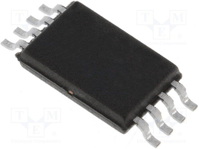
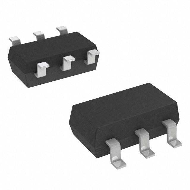
ICGOO电子元器件商城为您提供SI6926ADQ-T1-E3由Vishay设计生产,在icgoo商城现货销售,并且可以通过原厂、代理商等渠道进行代购。 SI6926ADQ-T1-E3价格参考。VishaySI6926ADQ-T1-E3封装/规格:晶体管 - FET,MOSFET - 阵列, 2 个 N 沟道(双) Mosfet 阵列 20V 4.1A 830mW 表面贴装 8-TSSOP。您可以下载SI6926ADQ-T1-E3参考资料、Datasheet数据手册功能说明书,资料中有SI6926ADQ-T1-E3 详细功能的应用电路图电压和使用方法及教程。
Vishay Siliconix 的 SI6926ADQ-T1-E3 是一款双通道 N 沟道增强型 MOSFET 阵列,广泛应用于各种电力电子场景。以下是其主要应用场景:

 1. 电源管理
   - 负载开关:SI6926ADQ-T1-E3 可用于控制电路中的负载通断,实现高效的负载切换。
   - DC-DC 转换器:在降压或升压转换器中作为开关元件,提供低导通电阻(Rds(on))以减少功率损耗。
   - 电池管理系统 (BMS):用于电池保护和充放电控制,确保电池安全运行。

 2. 电机驱动
   - 小型电机控制:适用于消费电子、家用电器中的小功率电机驱动,如风扇、泵等。
   - H 桥电路:通过组合两个 MOSFET 实现双向电机控制。

 3. 信号切换
   - 多路复用/解复用:在需要切换不同信号路径的电路中使用,例如数据通信设备。
   - 音频信号切换:在音频设备中切换不同的输入源或输出路径。

 4. 便携式设备
   - 移动设备电源管理:用于智能手机、平板电脑和其他便携式设备中的电源管理模块。
   - USB 充电保护:在 USB 接口处提供过流保护和快速开关功能。

 5. 汽车电子
   - 车载信息娱乐系统:用于音频放大器、显示屏背光控制等。
   - LED 照明驱动:为车内 LED 灯提供高效驱动和调光功能。
   - 车身控制系统:如车窗升降、座椅调节等小功率应用。

 6. 工业自动化
   - 传感器接口:用于工业传感器信号的开关和隔离。
   - 继电器替代:在需要快速响应和高可靠性的场合,替代传统机械继电器。

 特性优势
- 低导通电阻:降低功耗,提高效率。
- 高电流能力:支持较大的负载电流。
- 紧凑封装:适合空间受限的设计。
- 出色的热性能:有助于提升系统的稳定性和可靠性。

综上所述,SI6926ADQ-T1-E3 凭借其高性能和灵活性,适用于多种电力电子和信号处理场景,尤其在便携式设备、汽车电子和工业自动化领域表现出色。
| 参数 | 数值 |
| 产品目录 | |
| ChannelMode | Enhancement |
| 描述 | MOSFET 2N-CH 20V 4.1A 8TSSOPMOSFET DUAL N-CH 2.5V (G-S) |
| 产品分类 | FET - 阵列分离式半导体 |
| FET功能 | 逻辑电平门 |
| FET类型 | 2 个 N 沟道(双) |
| Id-ContinuousDrainCurrent | 4.1 A |
| Id-连续漏极电流 | 4.1 A |
| 品牌 | Vishay / SiliconixVishay Siliconix |
| 产品手册 | |
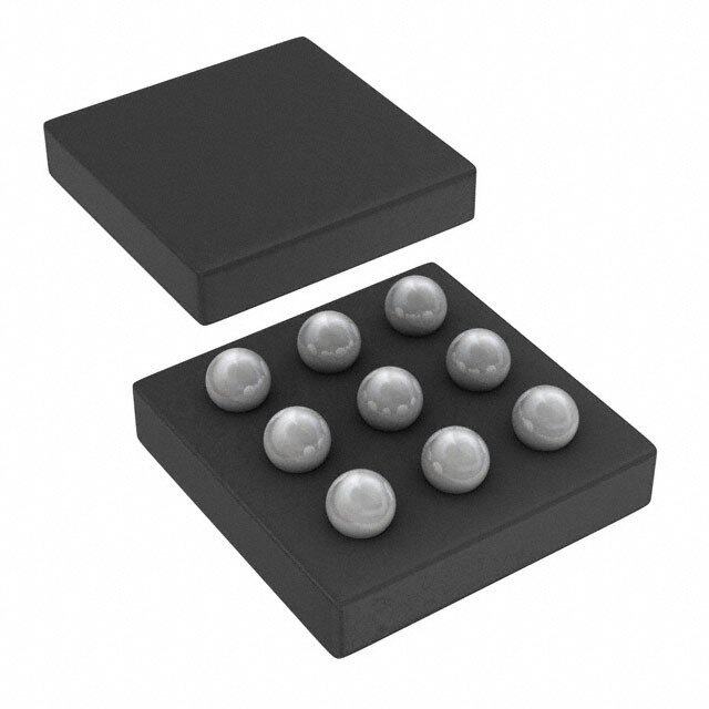
| 产品图片 |
|
| rohs | RoHS 合规性豁免无铅 / 符合限制有害物质指令(RoHS)规范要求 |
| 产品系列 | 晶体管,MOSFET,Vishay / Siliconix SI6926ADQ-T1-E3- |
| 数据手册 | |
| 产品型号 | SI6926ADQ-T1-E3SI6926ADQ-T1-E3 |
| Pd-PowerDissipation | 830 mW |
| Pd-功率耗散 | 830 mW |
| RdsOn-Drain-SourceResistance | 30 mOhms |
| RdsOn-漏源导通电阻 | 30 mOhms |
| Vds-Drain-SourceBreakdownVoltage | 20 V |
| Vds-漏源极击穿电压 | 20 V |
| Vgs-Gate-SourceBreakdownVoltage | +/- 8 V |
| Vgs-栅源极击穿电压 | 8 V |
| 上升时间 | 16 ns |
| 下降时间 | 16 ns |
| 不同Id时的Vgs(th)(最大值) | 1V @ 250µA |
| 不同Vds时的输入电容(Ciss) | - |
| 不同Vgs时的栅极电荷(Qg) | 10.5nC @ 4.5V |
| 不同 Id、Vgs时的 RdsOn(最大值) | 30 毫欧 @ 4.5A,4.5V |
| 产品目录页面 | |
| 产品种类 | MOSFET |
| 供应商器件封装 | 8-TSSOP |
| 其它名称 | SI6926ADQ-T1-E3DKR |
| 典型关闭延迟时间 | 46 ns |
| 功率-最大值 | 830mW |
| 包装 | Digi-Reel® |
| 商标 | Vishay / Siliconix |
| 安装类型 | 表面贴装 |
| 安装风格 | SMD/SMT |
| 封装 | Reel |
| 封装/外壳 | 8-TSSOP(0.173",4.40mm 宽) |
| 封装/箱体 | TSSOP-8 |
| 工厂包装数量 | 3000 |
| 晶体管极性 | N-Channel |
| 最大工作温度 | + 150 C |
| 最小工作温度 | - 55 C |
| 标准包装 | 1 |
| 漏源极电压(Vdss) | 20V |
| 电流-连续漏极(Id)(25°C时) | 4.1A |
| 系列 | SI6926ADQ |
| 通道模式 | Enhancement |
| 配置 | Dual |
| 零件号别名 | SI6926ADQ-E3 |


PDF Datasheet 数据手册内容提取
Si6926ADQ Vishay Siliconix Dual N-Channel 2.5-V (G-S) MOSFET FEATURES PRODUCT SUMMARY • Halogen-free V (V) R (Ω) I (A) DS DS(on) D 0.030 at VGS = 4.5 V 4.5 RoHS 0.033 at VGS = 3.0 V 4.2 COMPLIANT 20 0.035 at VGS = 2.5 V 3.9 0.043 at VGS = 1.8 V 3.6 D1 D2 TSSOP-8 D1 1 8 D2 G1 G2 S1 2 7 S2 S1 3 6 S2 G1 4 5 G2 Top View S1 S2 Ordering Information: Si6926ADQ-T1-GE3 (Lead (Pb)-free and Halogen-free) N-Channel MOSFET N-Channel MOSFET ABSOLUTE MAXIMUM RATINGS T = 25 °C, unless otherwise noted A Parameter Symbol 10 s Steady State Unit Drain-Source Voltage VDS 20 V Gate-Source Voltage VGS ± 8 Continuous Drain Current (TJ = 150 °C)a TTAA == 2750 °°CC ID 43..56 43..13 A Pulsed Drain Current (10 µs Pulse Width) IDM 20 Continuous Source Current (Diode Conduction)a IS 0.83 0.69 TA = 25 °C 1.0 0.83 Maximum Power Dissipationa PD W TA = 70 °C 0.64 0.53 Operating Junction and Storage Temperature Range TJ, Tstg - 55 to 150 °C THERMAL RESISTANCE RATINGS Parameter Symbol Typical Maximum Unit t ≤ 10 s 90 125 Maximum Junction-to-Ambienta RthJA Steady State 126 150 °C/W Maximum Junction-to-Foot (Drain) Steady State RthJF 65 80 Notes: a. Surface Mounted on FR4 board, t ≤ 10 s. For SPICE model information via the Worldwide Web: http://www.vishay.com/www/product/spice.htm. * Pb containing terminations are not RoHS compliant, exemptions may apply. Document Number: 72754 www.vishay.com S-81056-Rev. B, 12-May-08 1
Si6926ADQ Vishay Siliconix SPECIFICATIONS T = 25 °C, unless otherwise noted J Parameter Symbol Test Conditions Min. Typ.a Max. Unit Static Gate Threshold Voltage VGS(th) VDS = VGS, ID = 250 µA 0.40 1.0 V Gate-Body Leakage IGSS VDS = 0 V, VGS = ± 8 V ± 100 nA VDS = 20 V, VGS = 0 V 1 Zero Gate Voltage Drain Current IDSS µA VDS = 20 V, VGS = 0 V, TJ = 55 °C 5 On-State Drain Currentb ID(on) VDS ≥ 5 V, VGS = 5 V 10 A VGS = 4.5 V, ID = 4.5 A 0.024 0.030 VGS = 3.0 V, ID = 4.2 A 0.026 0.033 Drain-Source On-State Resistanceb RDS(on) Ω VGS = 2.5 V, ID = 3.9 A 0.029 0.035 VGS = 1.8 V, ID = 3.6 A 0.035 0.043 Forward Transconductanceb gfs VDS = 10 V, ID = 4.5 A 26 S Diode Forward Voltageb VSD IS = 0.83 A, VGS = 0 V 0.6 1.1 V Dynamica Total Gate Charge Qg 7.5 10.5 Gate-Source Charge Qgs VDS = 10 V, VGS = 4.5 V, ID = 4.5 A 1.2 nC Gate-Drain Charge Qgd 1.2 Gate Resistance Rg 1.9 Ω Turn-On Delay Time td(on) 6 12 Rise Time tr VDD = 10 V, RL = 10 Ω 16 25 Turn-Off Delay Time td(off) ID ≅ 1 A, VGEN = 10 V, Rg = 6 Ω 46 70 ns Fall Time tf 9 15 Source-Drain Reverse Recovery Time trr IF = 0.83 A, dI/dt = 100 A/µs 20 40 Notes: a. Guaranteed by design, not subject to production testing. b. Pulse test; pulse width ≤ 300 µs, duty cycle ≤ 2 %. Stresses beyond those listed under “Absolute Maximum Ratings” may cause permanent damage to the device. These are stress ratings only, and functional operation of the device at these or any other conditions beyond those indicated in the operational sections of the specifications is not implied. Exposure to absolute maximum rating conditions for extended periods may affect device reliability. TYPICAL CHARACTERISTICS 25°C, unless otherwise noted 20 20 VGS = 5 thru 2 V 16 16 A) A) Current ( 12 1.5 V Current ( 12 Drain 8 Drain 8 - - TC = 125 °C D D I 4 I 4 25 °C - 55 °C 0 0 0 1 2 3 4 5 0.00 0.25 0.50 0.75 1.00 1.25 1.50 1.75 2.00 VDS - Drain-to-Source Voltage (V) VGS -Gate-to-Source Voltage (V) Output Characteristics Transfer Characteristics www.vishay.com Document Number: 72754 2 S-81056-Rev. B, 12-May-08
Si6926ADQ Vishay Siliconix TYPICAL CHARACTERISTICS 25°C, unless otherwise noted 0.05 1200 1000 stance ()Ω 00..0034 VGS = 2.5 V VGS = 3.0 V ance (pF) 800 Ciss On-Resi 0.02 V = 4.5 V Capacit 600 -n) GS C - 400 o S( D R 0.01 200 Coss 0.00 0 Crss 0.0 4.0 8.0 12.0 16.0 20.0 0 4 8 12 16 20 ID -Drain Current (A) VDS -Drain-to-Source Voltage (V) On-Resistance vs. Drain Current Capacitance 6 1.6 VDS = 10 V VGS = 4.5 V e (V) 5 ID = 4.5 A 1.4 ID = 4.5 A g Gate-to-Source Volta 234 -On-ResistanceS(on)(Normalized) 11..02 - D S R G V 0.8 1 0 0.6 0 2 4 6 8 10 -50 -25 0 25 50 75 100 125 150 Qg -Total Gate Charge (nC) TJ - Junction Temperature (°C) Gate Charge On-Resistance vs. Junction Temperature 0.08 20 0.07 10 TJ = 150 °C )Ω 0.06 urrent (A) sistance ( 0.05 ID = 4.5 A urce C On-Re 0.04 -SoIS -DS(on) 00..0023 R TJ = 25 °C 0.01 1 0.00 0.0 0.2 0.4 0.6 0.8 1.0 1.2 0 1 2 3 4 5 6 7 8 VSD -Source-to-Drain Voltage (V) VGS -Gate-to-Source Voltage (V) Source-Drain Diode Forward Voltage On-Resistance vs. Gate-to-Source Voltage Document Number: 72754 www.vishay.com S-81056-Rev. B, 12-May-08 3
Si6926ADQ Vishay Siliconix TYPICAL CHARACTERISTICS 25°C, unless otherwise noted 0.2 30 0.1 25 ID = 250 µA nce (V) 0.0 W) 20 Varia -0.1 wer ( 15 h) Po S(t G -0.2 10 V -0.3 5 -0.4 0 -50 -25 0 25 50 75 100 125 150 10-3 10-2 10-1 1 10 100 600 TJ - Temperature (°C) Time (s) Threshold Voltage Single Pulse Power Junction-to-Ambient 100 Limited IDM Limited by R * DS(on) 10 A) nt ( 1 ms e urr 1 10 ms C ain ID(on) Dr Limited 100 ms - D I 0.1 TA = 25 °C 1 s Single Pulse 10 s DC 0.01 BVDSS Limited 0.1 1 10 100 VDS -Drain-to-SourceVoltage(V) *VGS>minimumVGSatwhichRDS(on)isspecified Safe Operating Area, Junction-to-Case 2 1 nt Duty Cycle = 0.5 e e Transiedance 0.2 ctivmp Notes: ed Effeermal I 0.1 0.1 PDM malizTh 0.05 t1 Nor 0.02 1. Duty Cyclet,2 D = t1 t2 2. Per Unit Base = RthJA = 126 °C/W Single Pulse 3. TJM - TA = PDMZthJA(t) 4. Surface Mounted 0.01 10-4 10-3 10-2 10-1 1 10 100 600 Square Wave Pulse Duration (s) Normalized Thermal Transient Impedance, Junction-to-Ambient www.vishay.com Document Number: 72754 4 S-81056-Rev. B, 12-May-08
Si6926ADQ Vishay Siliconix TYPICAL CHARACTERISTICS 25°C, unless otherwise noted 2 1 nt Duty Cycle = 0.5 e ctive Transimpedance 0.2 ed Effeermal I 0.1 0.1 zh aliT 0.05 m Nor 0.02 Single Pulse 0.01 10-4 10-3 10-2 10-1 1 10 Square Wave Pulse Duration (s) Normalized Thermal Transient Impedance, Junction-to-Foot Vishay Siliconix maintains worldwide manufacturing capability. Products may be manufactured at one of several qualified locations. Reliability data for Silicon Technology and Package Reliability represent a composite of all qualified locations. For related documents such as package/tape drawings, part marking, and reliability data, see http://www.vishay.com/ppg?72754. Document Number: 72754 www.vishay.com S-81056-Rev. B, 12-May-08 5
Package Information Vishay Siliconix (cid:1)(cid:2)(cid:2)(cid:3)(cid:4)(cid:5)(cid:6)(cid:6)(cid:6)(cid:6)(cid:7)(cid:8)(cid:9)(cid:10)(cid:11)(cid:12) JEDEC Part Number: MO-153 (cid:13)(cid:14)(cid:9)(cid:9)(cid:14)(cid:13)(cid:10)(cid:1)(cid:10)(cid:15)(cid:2) Dim Min Nom Max A – – 1.20 A1 0.05 0.10 0.15 E1 A2 0.80 1.00 1.05 B 0.19 0.28 0.30 C – 0.127 – D 2.90 3.00 3.10 e) E 6.20 6.40 6.60 n a Pl E1 4.30 4.40 4.50 e R 0.10 D ag e – 0.65 – Corners) e E 5 (G L 0.45 0.60 0.75 AA2 C 0.2 L1 0.90 1.00 1.10 Y – – 0.10 A1 B R 0.10 L (cid:1)K1 (cid:1)K1 0(cid:2) 3(cid:2) 6(cid:2) (4 Corners) L1 ECN: S-03946—Rev. G, 09-Jul-01 DWG: 5844 Document Number: 71201 www.vishay.com 06-Jul-01 1
AN1001 Vishay Siliconix (cid:1) LITTLE FOOT TSSOP-8 The Next Step in Surface-Mount Power MOSFETs Wharton McDaniel and David Oldham When Vishay Siliconix introduced its LITTLE FOOT This is the low profile demanded by applications such as MOSFETs, it was the first time that power MOSFETs had been PCMCIA cards. offered in a true surface-mount package, the SOIC. LITTLE FOOT immediately found a home in new small form factor disk It reduces the power package to the same height as many drives, computers, and cellular phones. resistors and capacitors in 0805 and 0605 sizes. It also allows placement on the “passive” side of the PC board. The new LITTLE FOOT TSSOP-8 power MOSFETs are the natural evolutionary response to the continuing demands of The standard pinouts of the LITTLE FOOT TSSOP-8 many markets for smaller and smaller packages. LITTLE packages have been changed from the standard established FOOT TSSOP-8 MOSFETs have a smaller footprint and a by LITTLE FOOT. This change minimizes the contribution of lower profile than LITTLE FOOT SOICs, while maintaining low interconnection resistance to rDS(on) and maximizes the r and high thermal performance. Vishay Siliconix has transfer of heat out of the package. DS(on) accomplished this by putting one or two high-density MOSFET die in a standard 8-pin TSSOP package mounted on a custom Figure 2 shows the pinouts for a single-die TSSOP. Notice that leadframe. both sides of the package have Source and Drain connections, whereas LITTLE FOOT has the Source and Gate connections on one side of the package, and the Drain connections are on the opposite side. THE TSSOP-8 PACKAGE LITTLE FOOT TSSOP-8 power MOSFETs require approximately half the PC board area of an equivalent LITTLE Drain Drain FOOT device (Figure 1). In addition to the reduction in board Source Source area, the package height has been reduced to 1.1 mm. Source Source Gate Drain Figure 2. Pinouts for Single Die TSSOP Figure 3 shows the standard pinouts for a dual-die TSSOP-8. In this case, the connections for each individual MOSFET Top View occupy one side. Drain 1 Drain 2 Source 1 Source 2 Side View Source 1 Source 2 Gate 1 Gate 2 Figure 1. An TSSOP-8 Package Next to a SOIC-8 Package with Views from Both Top and Side Figure 3. Pinouts for Dual-Die TSSOP Document Number: 70571 www.vishay.com 12-Dec-03 1
AN1001 Vishay Siliconix Because the TSSOP has a fine pitch foot print, the pad layout is somewhat more demanding than the layout of the SOIC. Careful attention must be paid to silkscreen-to-pad and soldermask-to-pad clearances. Also, fiduciary marks may be required. The design and spacing of the pads must be dealt with carefully. The pads must be sized to hold enough solder paste to form a good joint, but should not be so large or so placed as to extend under the body, increasing the potential for Figure 5. solder bridging. The pad pattern should allow for typical pick and place errors of 0.25 mm. See Application Note 826, The actual test is based on dissipating a known amount of Recommended Minimum Pad Patterns With Outline power in the device for a known period of time so the junction Drawing Access for Vishay Siliconix MOSFETs, temperature is raised to 150(cid:2)C. The starting and ending (http://www.vishay.com/doc?72286), for the recommended junction temperatures are determined by measuring the pad pattern for PC board layout. forward drop of the body diode. The thermal resistance for that pulse width is defined by the temperature rise of the junction THERMAL ISSUES above ambient and the power of the pulse, (cid:1)Tja/P. Figure 6 shows the single pulse power curve of the Si6436DQ LITTLE FOOT TSSOP MOSFETs have been given thermal laid over the curve of the Si9936DY to give a comparison of the ratings using the same methods used for LITTLE FOOT. The thermal performance. The die in the two devices have maximum thermal resistance junction-to-ambient is 83(cid:2)C/W equivalent die areas, making this a comparison of the for the single die and 125(cid:2)C/W for dual-die parts. TSSOP relies packaging. This comparison shows that the TSSOP package on a leadframe similar to LITTLE FOOT to remove heat from performs as well as the SOIC out to 150 ms, with long-term the package. The single- and dual-die leadframes are shown performance being 0.5 W less. Although the thermal in Figure 4. performance is less, LITTLE FOOT TSSOP will operate in a large percentage of applications that are currently being served by LITTLE FOOT. 14.0 12.0 10.0 a) 8-Pin Single-Pad TSSOP W) 8.0 er ( w Po 6.0 4.0 Si9936 2.0 Si6436 0.0 0.1 1 10 100 b) 8-Pin Dual-Pad TSSOP Time (Sec.) Figure 6. Comparison of Thermal Performance Figure 4. Leadframe CONCLUSION The MOSFETs are characterized using a single pulse power test. For this test the device mounted on a one-square-inch piece of copper clad FR-4 PC board, such as those shown in TSSOP power MOSFETs provide a significant reduction in PC Figure 5. The single pulse power test determines the board footprint and package height, allowing reduction in maximum amount of power the part can handle for a given board size and application where SOICs will not fit. This is pulse width and defines the thermal resistance accomplished using a standard IC package and a custom junction-to-ambient. The test is run for pulse widths ranging leadframe, combining small size with good power handling from approximately 10 ms to 100 seconds. The thermal capability. resistance at 30 seconds is the rated thermal resistance for the part. This rating was chosen to allow comparison of packages For the TSSOP-8 package outline visit: and leadframes. At longer pulse widths, the PC board thermal http://www.vishay.com/doc?71201 charateristics become dominant, making all parts look the For the SOIC-8 package outline visit: same. http://www.vishay.com/doc?71192 www.vishay.com Document Number: 70571 2 12-Dec-03
AN806 Vishay Siliconix (cid:1) Mounting LITTLE FOOT TSSOP-8 Power MOSFETs Wharton McDaniel Surface-mounted LITTLE FOOT power MOSFETs use integrated The pad patterns with copper spreading for the single-MOSFET circuit and small-signal packages which have been been modified TSSOP-8 (Figure 1) and dual-MOSFET TSSOP-8 (Figure 2) to provide the heat transfer capabilities required by power devices. show the starting point for utilizing the board area available for the Leadframe materials and design, molding compounds, and die heat-spreading copper. To create this pattern, a plane of copper attach materials have been changed, while the footprint of the overlies the drain pins. The copper plane connects the drain pins packages remains the same. electrically, but more importantly provides planar copper to draw heat from the drain leads and start the process of spreading the heat so it can be dissipated into the ambient air. These patterns use all the available area underneath the body for this purpose. See Application Note 826, Recommended Minimum Pad Patterns With Outline Drawing Access for Vishay Siliconix MOSFET, (http://www.vishay.com/doc?72286), for the basis of the pad design for a LITTLE FOOT TSSOP-8 power MOSFET 0.284 7.6 package footprint. In converting the footprint to the pad set for a power device, designers must make two connections: an electrical 0.032 0.8 connection and a thermal connection, to draw heat away from the 0.026 0.122 package. 0.66 3.1 0.018 0.45 0.073 0.091 In the case of the TSSOP-8 package, the thermal connections 1.78 1.65 are very simple. Pins 1, 5, and 8 are the drain of the MOSFET for a single MOSFET package and are connected together. In FIGURE 2. Dual MOSFET TSSOP-8 Pad Pattern with the dual package, pins 1 and 8 are the two drains. For a Copper Spreading small-signal device or integrated circuit, typical connections would be made with traces that are 0.020 inches wide. Since the drain pins also provide the thermal connection to the Since surface-mounted packages are small, and reflow soldering package, this level of connection is inadequate. The total is the most common way in which these are affixed to the PC cross section of the copper may be adequate to carry the board, “thermal” connections from the planar copper to the pads current required for the application, but it presents a large have not been used. Even if additional planar copper area is used, thermal impedance. Also, heat spreads in a circular fashion there should be no problems in the soldering process. The actual from the heat source. In this case the drain pins are the heat solder connections are defined by the solder mask openings. By sources when looking at heat spread on the PC board. combining the basic footprint with the copper plane on the drain pins, the solder mask generation occurs automatically. 0.284 A final item to keep in mind is the width of the power traces. The 7.6 absolute minimum power trace width must be determined by the 0.032 amount of current it has to carry. For thermal reasons, this 0.8 minimum width should be at least 0.020 inches. The use of wide 0.026 0.122 0.66 3.1 traces connected to the drain plane provides a low impedance 0.018 path for heat to move away from the device. 0.45 0.073 0.118 1.78 3.54 FIGURE 1. Single MOSFET TSSOP-8 Pad Pattern with Copper Spreading Document Number: 70738 www.vishay.com 17-Dec-03 1
Application Note 826 Vishay Siliconix RECOMMENDED MINIMUM PADS FOR TSSOP-8 0.092 (2.337) 0.026 (0.660) 2 5) 2 3) 6 5 8 2 2 6 1 6 0. 6. 0. 4. ( ( 0 6) 4 1 0 0 0. 1. ( 0.014 0.012 (0.356) (0.305) Recommended Minimum Pads Dimensions in Inches/(mm) Return to Index Return to Index A P P L I C A T I O N N O T E Document Number: 72611 www.vishay.com Revision: 21-Jan-08 27
Legal Disclaimer Notice www.vishay.com Vishay Disclaimer ALL PRODUCT, PRODUCT SPECIFICATIONS AND DATA ARE SUBJECT TO CHANGE WITHOUT NOTICE TO IMPROVE RELIABILITY, FUNCTION OR DESIGN OR OTHERWISE. Vishay Intertechnology, Inc., its affiliates, agents, and employees, and all persons acting on its or their behalf (collectively, “Vishay”), disclaim any and all liability for any errors, inaccuracies or incompleteness contained in any datasheet or in any other disclosure relating to any product. Vishay makes no warranty, representation or guarantee regarding the suitability of the products for any particular purpose or the continuing production of any product. To the maximum extent permitted by applicable law, Vishay disclaims (i) any and all liability arising out of the application or use of any product, (ii) any and all liability, including without limitation special, consequential or incidental damages, and (iii) any and all implied warranties, including warranties of fitness for particular purpose, non-infringement and merchantability. Statements regarding the suitability of products for certain types of applications are based on Vishay’s knowledge of typical requirements that are often placed on Vishay products in generic applications. Such statements are not binding statements about the suitability of products for a particular application. It is the customer’s responsibility to validate that a particular product with the properties described in the product specification is suitable for use in a particular application. Parameters provided in datasheets and / or specifications may vary in different applications and performance may vary over time. All operating parameters, including typical parameters, must be validated for each customer application by the customer’s technical experts. Product specifications do not expand or otherwise modify Vishay’s terms and conditions of purchase, including but not limited to the warranty expressed therein. Except as expressly indicated in writing, Vishay products are not designed for use in medical, life-saving, or life-sustaining applications or for any other application in which the failure of the Vishay product could result in personal injury or death. Customers using or selling Vishay products not expressly indicated for use in such applications do so at their own risk. Please contact authorized Vishay personnel to obtain written terms and conditions regarding products designed for such applications. No license, express or implied, by estoppel or otherwise, to any intellectual property rights is granted by this document or by any conduct of Vishay. Product names and markings noted herein may be trademarks of their respective owners. © 2017 VISHAY INTERTECHNOLOGY, INC. ALL RIGHTS RESERVED Revision: 08-Feb-17 1 Document Number: 91000
Mouser Electronics Authorized Distributor Click to View Pricing, Inventory, Delivery & Lifecycle Information: V ishay: SI6926ADQ-T1-E3