ICGOO在线商城 > 分立半导体产品 > 晶体管 - FET,MOSFET - 阵列 > FDC8602
 Datasheet下载
- 型号: FDC8602
- 制造商: Fairchild Semiconductor
- 库位|库存: xxxx|xxxx
- 要求:
| 数量阶梯 | 香港交货 | 国内含税 |
| +xxxx | $xxxx | ¥xxxx |
查看当月历史价格
查看今年历史价格
FDC8602产品简介:
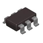
ICGOO电子元器件商城为您提供FDC8602由Fairchild Semiconductor设计生产,在icgoo商城现货销售,并且可以通过原厂、代理商等渠道进行代购。 FDC8602价格参考。Fairchild SemiconductorFDC8602封装/规格:晶体管 - FET,MOSFET - 阵列, 2 个 N 沟道(双) Mosfet 阵列 100V 1.2A 690mW 表面贴装 SuperSOT™-6。您可以下载FDC8602参考资料、Datasheet数据手册功能说明书,资料中有FDC8602 详细功能的应用电路图电压和使用方法及教程。
FDC8602 是由 ON Semiconductor(安森美半导体)生产的晶体管阵列,属于 FET、MOSFET 类别。该器件是一款双通道 N 沟道 MOSFET 阵列,具有低导通电阻和快速开关特性,适用于多种应用场景。

 主要应用场景:

1. 电源管理:
   - FDC8602 适用于各种电源管理应用,如 DC-DC 转换器、负载开关和电池管理系统。其低导通电阻(Rds(on))可以减少功率损耗,提高效率,特别适合需要高效能的便携式设备,如智能手机、平板电脑和其他手持电子设备。

2. 电机控制:
   - 在小型电机控制中,FDC8602 可用于驱动步进电机、直流电机或无刷直流电机。其快速开关特性和低导通电阻有助于实现高效的电机驱动,同时减少发热,延长设备寿命。

3. 信号切换:
   - FDC8602 可用于信号切换电路,如多路复用器或多路选择器。它能够快速切换信号路径,适用于音频设备、视频切换器和其他需要高频率信号处理的应用。

4. 负载保护:
   - 在负载保护电路中,FDC8602 可以作为过流保护、短路保护或热保护的关键组件。其内置的保护功能可以在异常情况下迅速切断电流,防止损坏下游电路。

5. 消费电子产品:
   - 该器件广泛应用于消费电子产品中,如笔记本电脑、智能手表、智能家居设备等。其紧凑的封装和高效能使其成为这些设备的理想选择,能够在有限的空间内提供高性能和可靠性。

6. 工业自动化:
   - 在工业自动化领域,FDC8602 可用于传感器接口、继电器替代、PLC(可编程逻辑控制器)输入输出模块等。其坚固耐用的设计和宽工作温度范围(-55°C 至 +150°C)使其适合恶劣环境下的应用。

总之,FDC8602 凭借其出色的性能和广泛的适用性,在多个领域中都能发挥重要作用,特别是在需要高效能、小尺寸和可靠性的应用场景中表现尤为突出。
| 参数 | 数值 |
| 产品目录 | |
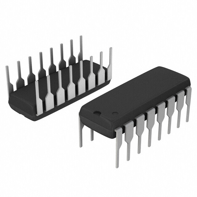
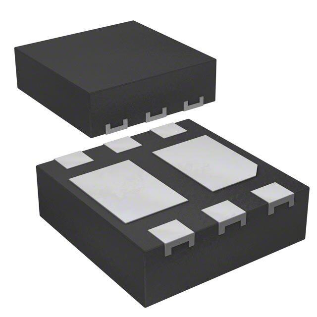
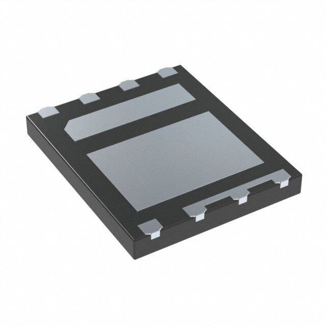
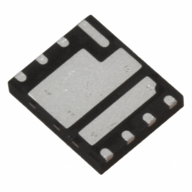
| 描述 | MOSFET 2N-CH 100V 1.2A 6-SSOTMOSFET NCH DUAL COOL POWERTRENCH MOSFET |
| 产品分类 | FET - 阵列分离式半导体 |
| FET功能 | 标准 |
| FET类型 | 2 个 N 沟道(双) |
| Id-ContinuousDrainCurrent | 1.2 A |
| Id-连续漏极电流 | 1.2 A |
| 品牌 | Fairchild Semiconductor |
| 产品手册 | |
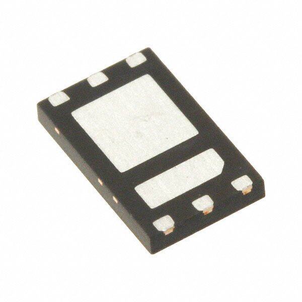
| 产品图片 |
|
| rohs | 符合RoHS无铅 / 符合限制有害物质指令(RoHS)规范要求 |
| 产品系列 | 晶体管,MOSFET,Fairchild Semiconductor FDC8602PowerTrench® |
| 数据手册 | |
| 产品型号 | FDC8602 |
| PCN封装 | |
| PCN组件/产地 | |
| Pd-PowerDissipation | 0.69 W |
| Pd-功率耗散 | 690 mW |
| RdsOn-Drain-SourceResistance | 350 mOhms |
| RdsOn-漏源导通电阻 | 350 mOhms |
| Vds-Drain-SourceBreakdownVoltage | 100 V |
| Vds-漏源极击穿电压 | 100 V |
| Vgs-Gate-SourceBreakdownVoltage | +/- 20 V |
| Vgs-栅源极击穿电压 | 20 V |
| 不同Id时的Vgs(th)(最大值) | 4V @ 250µA |
| 不同Vds时的输入电容(Ciss) | 70pF @ 50V |
| 不同Vgs时的栅极电荷(Qg) | 2nC @ 10V |
| 不同 Id、Vgs时的 RdsOn(最大值) | 350 毫欧 @ 1.2A,10V |
| 产品种类 | MOSFET |
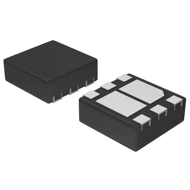
| 供应商器件封装 | 6-SSOT |
| 其它名称 | FDC8602TR |
| 功率-最大值 | 690mW |
| 包装 | 带卷 (TR) |
| 单位重量 | 36 mg |
| 商标 | Fairchild Semiconductor |
| 安装类型 | 表面贴装 |
| 安装风格 | SMD/SMT |
| 导通电阻 | 350 mOhms |
| 封装 | Reel |
| 封装/外壳 | SOT-23-6 细型,TSOT-23-6 |
| 封装/箱体 | SSOT-6 |
| 工厂包装数量 | 3000 |
| 晶体管极性 | N-Channel |
| 最大工作温度 | + 150 C |
| 最小工作温度 | - 55 C |
| 标准包装 | 3,000 |
| 汲极/源极击穿电压 | 100 V |
| 漏极连续电流 | 1.2 A |
| 漏源极电压(Vdss) | 100V |
| 电流-连续漏极(Id)(25°C时) | 1.2A |
| 系列 | FDC8602 |
| 配置 | Dual |


PDF Datasheet 数据手册内容提取
Is Now Part of To learn more about ON Semiconductor, please visit our website at www.onsemi.com Please note: As part of the Fairchild Semiconductor integration, some of the Fairchild orderable part numbers will need to change in order to meet ON Semiconductor’s system requirements. Since the ON Semiconductor product management systems do not have the ability to manage part nomenclature that utilizes an underscore (_), the underscore (_) in the Fairchild part numbers will be changed to a dash (-). This document may contain device numbers with an underscore (_). Please check the ON Semiconductor website to verify the updated device numbers. The most current and up-to-date ordering information can be found at www.onsemi.com. Please email any questions regarding the system integration to Fairchild_questions@onsemi.com. ON Semiconductor and the ON Semiconductor logo are trademarks of Semiconductor Components Industries, LLC dba ON Semiconductor or its subsidiaries in the United States and/or other countries. ON Semiconductor owns the rights to a number of patents, trademarks, copyrights, trade secrets, and other intellectual property. A listing of ON Semiconductor’s product/patent coverage may be accessed at www.onsemi.com/site/pdf/Patent-Marking.pdf. ON Semiconductor reserves the right to make changes without further notice to any products herein. ON Semiconductor makes no warranty, representation or guarantee regarding the suitability of its products for any particular purpose, nor does ON Semiconductor assume any liability arising out of the application or use of any product or circuit, and specifically disclaims any and all liability, including without limitation special, consequential or incidental damages. Buyer is responsible for its products and applications using ON Semiconductor products, including compliance with all laws, regulations and safety requirements or standards, regardless of any support or applications information provided by ON Semiconductor. “Typical” parameters which may be provided in ON Semiconductor data sheets and/or specifications can and do vary in different applications and actual performance may vary over time. All operating parameters, including “Typicals” must be validated for each customer application by customer’s technical experts. ON Semiconductor does not convey any license under its patent rights nor the rights of others. ON Semiconductor products are not designed, intended, or authorized for use as a critical component in life support systems or any FDA Class 3 medical devices or medical devices with a same or similar classification in a foreign jurisdiction or any devices intended for implantation in the human body. Should Buyer purchase or use ON Semiconductor products for any such unintended or unauthorized application, Buyer shall indemnify and hold ON Semiconductor and its officers, employees, subsidiaries, affiliates, and distributors harmless against all claims, costs, damages, and expenses, and reasonable attorney fees arising out of, directly or indirectly, any claim of personal injury or death associated with such unintended or unauthorized use, even if such claim alleges that ON Semiconductor was negligent regarding the design or manufacture of the part. ON Semiconductor is an Equal Opportunity/Affirmative Action Employer. This literature is subject to all applicable copyright laws and is not for resale in any manner.
F D C 8 6 May 2013 0 2 FDC8602 D u Dual N-Channel Shielded Gate PowerTrench® MOSFET a l N 100 V, 1.2 A, 350 mΩ - C Features General Description h a n (cid:132) Shielded Gate MOSFET Technology This N-Channel MOSFET is produced using Fairchild n e (cid:132) Max rDS(on) = 350 mΩ at VGS = 10 V, ID = 1.2 A Semiconductor‘s advanced PowerTrench® process that l S (cid:132) Max r = 575 mΩ at V = 6 V, I = 0.9 A incorporates Shielded Gate technology. This process has been h DS(on) GS D optimized for rDS(on), switching performance and ruggedness. ie (cid:132) High performance trench technology for extremely low rDS(on) ld (cid:132) High power and current handling capability in a widely used e d surface mount package G Applications (cid:132) Fast switching speed a t e (cid:132) 100% UIL Tested (cid:132) Load Switch P (cid:132) RoHS Compliant (cid:132) Synchronous Rectifier o w e r T r e n c h ® D2 M S1 O S D1 F E T G2 S2 Pin 1 G1 SuperSOTTM -6 MOSFET Maximum Ratings TA = 25 °C unless otherwise noted Symbol Parameter Ratings Units V Drain to Source Voltage 100 V DS V Gate to Source Voltage ±20 V GS Drain Current -Continuous (Note 1a) 1.2 A I D -Pulsed 5 A E Single Pulse Avalanche Energy (Note 3) 1.5 mJ AS Power Dissipation (Note 1a) 0.96 P W D Power Dissipation (Note 1b) 0.69 T , T Operating and Storage Junction Temperature Range -55 to +150 °C J STG Thermal Characteristics R Thermal Resistance, Junction to Case 60 θJC °C/W R Thermal Resistance, Junction to Ambient (Note 1a) 130 θJA Package Marking and Ordering Information Device Marking Device Package Reel Size Tape Width Quantity .862 FDC8602 SSOT-6 7 ’’ 8 mm 3000 units ©2011 Fairchild Semiconductor Corporation 1 www.fairchildsemi.com FDC8602 Rev.C1
F D Electrical Characteristics T = 25 °C unless otherwise noted C J 8 6 Symbol Parameter Test Conditions Min Typ Max Units 0 2 Off Characteristics D BV Drain to Source Breakdown Voltage I = 250 μA, V = 0 V 100 V u DSS D GS a Δ BΔVTDSS BCroeeaffkicdioewntn Voltage Temperature ID = 250 μA, referenced to 25 °C 73 mV/°C l N J - C I Zero Gate Voltage Drain Current V = 80 V, V = 0 V 1 μA DSS DS GS h IGSS Gate to Source Leakage Current VGS = ±20 V, VDS = 0 V ±100 nA a n n On Characteristics e VGS(th) Gate to Source Threshold Voltage VGS = VDS, ID = 250 μA 2 3.2 4 V l S Δ ΔVTGS(th) GTeamtep teor aStuoruer cCeo Tehffriceisehnotld Voltage ID = 250 μA, referenced to 25 °C -8 mV/°C hie J l d V = 10 V, I = 1.2 A 285 350 GS D e r Static Drain to Source On Resistance V = 6 V, I = 0.9 A 409 575 mΩ d DS(on) GS D G V = 10V, I = 1.2A, T = 125 °C 489 600 GS D J a gFS Forward Transconductance VDS = 10 V, ID = 1.2 A 1.3 S te P Dynamic Characteristics o w C Input Capacitance 53 70 pF iss V = 50 V, V = 0 V, e C Output Capacitance DS GS 17 25 pF r oss f = 1MHz T C Reverse Transfer Capacitance 0.8 5 pF r rss e R Gate Resistance 1.6 Ω n g c h Switching Characteristics ® M t Turn-On Delay Time 3.5 10 ns d(on) tr Rise Time VDD = 50 V, ID = 1.2 A, 1.7 10 ns OS td(off) Turn-Off Delay Time VGS = 10 V, RGEN = 6 Ω 5.4 11 ns F E t Fall Time 2.3 10 ns f T Q Total Gate Charge V = 0 V to 10 V 1.2 2 nC g(TOT) GS Qg(TOT) Total Gate Charge VGS = 0 V to 5 V VDD = 50 V, 0.6 1 nC Qgs Gate to Source Charge ID = 1.2 A 0.4 nC Q Gate to Drain “Miller” Charge 0.4 nC gd Drain-Source Diode Characteristics V Source-Drain Diode Forward Voltage V = 0 V, I = 1.2 A (Note 2) 0.86 1.3 V SD GS S trr Reverse Recovery Time I = 1.2 A, di/dt = 100 A/μs 27 43 ns Q Reverse Recovery Charge F 12 21 nC rr NOTES: 1. RθJA is the sum of the junction-to-case and case-to-ambient thermal resistance where the case thermal reference is defined as the solder mounting surface of the drain pins. RθJC is guaranteed by design while RθCA is determined by the user's board design. a) 130 °C/W when mounted on b) 180 °C/W when mounted on a a 1 in2 pad of 2 oz copper minimum pad of 2 oz copper 2. Pulse Test: Pulse Width < 300 μs, Duty cycle < 2.0%. 3. Starting TJ = 25 °C; N-ch: L = 3 mH, IAS = 1 A, VDD = 100 V, VGS = 10 V. ©2011 Fairchild Semiconductor Corporation 2 www.fairchildsemi.com FDC8602 Rev.C1
F D C 8 Typical Characteristics T = 25 °C unless otherwise noted 6 J 0 2 D 5 4 u AIN CURRENT (A) 234 VGS = 10 VPULSE DURVAGTSIO =N 8 = V 80 μs VVGGSS == 67 VV NORMALIZEDOURCE ON-RESISTANCE 23 VGS = 5 V VVGGSS = = 6 8 V VVGS = 7 V al N-Channel S DR DUTY CYCLE = 0.5% MAX O S 1 h I, D 01 VGS = 5 V DRAIN T 0 PDUULTSYE C DYUCRLEA T=I O0.N5 %= 8M0A μXs VGS = 10 V ielded 0 1 2 3 4 5 0 1 2 3 4 5 G VDS, DRAIN TO SOU RCE VOLTAGE (V) ID, DRAIN CURR ENT (A) a t e Figure 1. On Region Characteristics Figure 2. Normalized On-Resistance P vs Drain Current and Gate Voltage o w e r 2.0 1200 T r ANCE 1.8 IVDG =S 1=. 21 0A V )mΩ ID = 1.2 A PDUULTSYE C DYUCRLEA T=I O0.N5 %= 8M0A μXs enc NORMALIZED O SOURCE ON-RESIST 1111....0246 , rDRAIN TO DS(on) (CE ON-RESISTANCE369000000 TJ = 125 oC h MOSFET® N T 0.8 UR TJ = 25 oC RAI SO D 0.6 0 -75 -50 -25 0 25 50 75 100 125 150 5 6 7 8 9 10 TJ, JUNCTION TEM PERATURE (oC) VGS, GATE TO SOUR CE VOLTAGE (V) Figure 3. Normalized On Resistance Figure 4. On-Resistance vs Gate to vs Junction Temperature Source Voltage 5 10 PULSE DURATION = 80 μs A) VGS = 0 V DUTY CYCLE = 0.5% MAX T ( A) 4 VDS = 5 V REN 1 TJ = 150 oC T ( UR RREN 3 AIN C 0.1 TJ = 25 oC U R C D N 2 E DRAI TJ = 150 oC TJ = 25 oC VERS 0.01 , D 1 RE I , S TJ = -55 oC TJ = -55 oC I 0 0.001 2 3 4 5 6 7 8 0.2 0.4 0.6 0.8 1.0 1.2 VGS, GATE TO SOU RCE VOLTAGE (V) VSD, BODY DIODE FOR WARD VOLTAGE (V) Figure 5. Transfer Characteristics Figure 6. Source to Drain Diode Forward Voltage vs Source Current ©2011 Fairchild Semiconductor Corporation 3 www.fairchildsemi.com FDC8602 Rev.C1
F D Typical Characteristics T = 25 °C unless otherwise noted C J 8 6 0 2 10 500 D GE (V) 8 ID = 1.2 A VDD = 50 V Ciss ua TA l N CE VOL 6 VDD = 25 V VDD = 75 V CE (pF) 10 Coss -Ch SOUR 4 CITAN ann E TO CAPA 1 el AT 2 Crss S G f = 1 MHz h , GS VGS = 0 V ie V 0 0.1 ld 0 0.2 0.4 0.6 0.8 1.0 1.2 1.4 0.1 1 10 100 e Qg, GATE CH ARGE (nC) VDS, DRAIN TO SOU RCE VOLTAGE (V) d G a Figure 7. Gate Charge Characteristics Figure 8. Capacitance vs Drain t e to Source Voltage P o w 2 10 e r T A) re T ( 1 A) n REN TJ = 25 oC NT ( 1 100 us ch UR RE ® E C TJ = 100 oC CUR THIS AREA IS 1 ms M NCH AIN 0.1 LIMITED BY rDS(on) 10 ms OS LA DR SINGLE PULSE F VA , D TJ = MAX RATED 100 ms E I, AAS TJ = 125 oC I0.01 TRAθJ =A 2=5 1 o8C0 oC/W 1D10C ss T 0.1 0.005 0.01 0.1 1 10 0.1 1 10 100 400 tAV, TIME IN AVA LANCHE (ms) VDS, DRAIN to SOU RCE VOLTAGE (V) Figure 9. Unclamped Inductive Figure 10. Forward Bias Safe Switching Capability Operating Area W) 100 VGS = 10 V SINGLE PULSE R ( RθJA = 180 oC/W E W T = 25 oC O A P T N E 10 NSI A R T K A E P , K) 1 P P( 0.5 10-4 10-3 10-2 10-1 1 10 100 1000 t, PULSE WIDTH (s ec) Figure 11. Single Pulse Maximum Power Dissipation ©2011 Fairchild Semiconductor Corporation 4 www.fairchildsemi.com FDC8602 Rev.C1
F D Typical Characteristics T = 25 °C unless otherwise noted C J 8 6 0 2 2 DUTY CYCLE-DESCENDING ORDER D 1 u D = 0.5 a MAL A 00..21 l N ERZJθ 0.05 -C D TH NCE, 0.1 00..0021 PDM ha LIZEEDA nn MAMP t1 e ORI t2 l S N SINGLE PULSE NOTES: 0.01 RθJA = 180 oC/W DPEUATKY FTAJ C= TPODRM: xD Z =θ JtA1 /xt2 RθJA + TA hie l d 0.005 e 10-4 10-3 10-2 10-1 1 10 100 1000 d t, RECTANGULAR PULSE DURATION (sec) G a Figure 12. Junction-to-Ambient Transient Thermal Response Curve t e P o w e r T r e n c h ® M O S F E T ©2011 Fairchild Semiconductor Corporation 5 www.fairchildsemi.com FDC8602 Rev.C1
F D Dimensional Outline and Pad Layout C 8 6 0 2 D u a l N - C h a n n e l S h i e l d e d G a t e P o w e r T r e n c h ® M O S F E T ©2011 Fairchild Semiconductor Corporation 6 www.fairchildsemi.com FDC8602 Rev.C1
F D C 8 6 0 2 D TRADEMARKS u The following includes registered and unregistered trademarks and service marks, owned by Fairchild Semiconductor and/or its global subsidiaries, and is not a intended to be an exhaustive list of all such trademarks. l N 2Cool™ FPS™ Sync-Lock™ - AccuPower™ F-PFS™ ® ®* C AX-CAP®* FRFET® PowtmerTrench® h BitSiC™ Global Power ResourceSM PowerXS™ a Build it Now™ Green Bridge™ Programmable Active Droop™ TinyBoost™ n CorePLUS™ Green FPS™ QFET® TinyBuck™ n TinyCalc™ e CCoRrOePSOSVWOELRT™™ GGmreaexn™ FPS™ e-Series™ QQuSi™et Series™ TTIinNyYLOogPiTc®O™ l S CTL™ GTO™ RapidConfigure™ TinyPower™ h Current Transfer Logic™ IntelliMAX™ ™ i DDEcuEoaUSl XCPPAoEoREl™KD®® IMaSnaOdr kPBiLneAgtt NeSrAm™Ra™ll Speakers Sound Louder SSiagvninaglW oiuser ™world, 1mW/W/kW at a time™ TTTiirnnayynWPSWiiCreM®™™ elde TriFault Detect™ d EESffiBceCn™tMax™ MMeICgRaBOuCcOk™UPLER™ SSMmAarRtMTa SxT™ART™ TRUECURRENT®* G μSerDes™ MicroFET™ Solutions for Your Success™ a ® MicroPak™ SPM® te FFFFAaAaiiCCrrccTThh ®iiQllddu® Sieetm Siecroiensd™uctor® MMMmiioWcllteriSoorDnaPMvraievkare2x™™™™ SSSSTuuupppEeeeArrrLFSSTEOOHTTT™®™™--36 UUUlHntriCFa E®FTR™FET™ Pow FFaAsStvTC®ore™ OOPptToOHLiTO™GIC® SSuuppererMSOOTS™®-8 VVCisuXa™lMax™ erT FETBench™ OPTOPLANAR® SyncFET™ VXoSl™tagePlus™ re n c h *Trademarks of System General Corporation, used under license by Fairchild Semiconductor. ® DISCLAIMER M FAIRCHILD SEMICONDUCTOR RESERVES THE RIGHT TO MAKE CHANGES WITHOUT FURTHER NOTICE TO ANY PRODUCTS HEREIN TO IMPROVE O RELIABILITY, FUNCTION, OR DESIGN. FAIRCHILD DOES NOT ASSUME ANY LIABILITY ARISING OUT OF THE APPLICATION OR USE OF ANY S PRODUCT OR CIRCUIT DESCRIBED HEREIN; NEITHER DOES IT CONVEY ANY LICENSE UNDER ITS PATENT RIGHTS, NOR THE RIGHTS OF OTHERS. F THESE SPECIFICATIONS DO NOT EXPAND THE TERMS OF FAIRCHILD’S WORLDWIDE TERMS AND CONDITIONS, SPECIFICALLY THE WARRANTY E THEREIN, WHICH COVERS THESE PRODUCTS. T LIFE SUPPORT POLICY FAIRCHILD’S PRODUCTS ARE NOT AUTHORIZED FOR USE AS CRITICAL COMPONENTS IN LIFE SUPPORT DEVICES OR SYSTEMS WITHOUT THE EXPRESS WRITTEN APPROVAL OF FAIRCHILD SEMICONDUCTOR CORPORATION. As used here in: 1. Life support devices or systems are devices or systems which, (a) are 2. A critical component in any component of a life support, device, or intended for surgical implant into the body or (b) support or sustain life, system whose failure to perform can be reasonably expected to cause and (c) whose failure to perform when properly used in accordance with the failure of the life support device or system, or to affect its safety or instructions for use provided in the labeling, can be reasonably effectiveness. expected to result in a significant injury of the user. ANTI-COUNTERFEITING POLICY Fairchild Semiconductor Corporation’s Anti-Counterfeiting Policy. Fairchild’s Anti-Counterfeiting Policy is also stated on our external website, www.Fairchildsemi.com, under Sales Support. Counterfeiting of semiconductor parts is a growing problem in the industry. All manufactures of semiconductor products are experiencing counterfeiting of their parts. Customers who inadvertently purchase counterfeit parts experience many problems such as loss of brand reputation, substandard performance, failed application, and increased cost of production and manufacturing delays. Fairchild is taking strong measures to protect ourselves and our customers from the proliferation of counterfeit parts. Fairchild strongly encourages customers to purchase Fairchild parts either directly from Fairchild or from Authorized Fairchild Distributors who are listed by country on our web page cited above. Products customers buy either from Fairchild directly or from Authorized Fairchild Distributors are genuine parts, have full traceability, meet Fairchild’s quality standards for handing and storage and provide access to Fairchild’s full range of up-to-date technical and product information. Fairchild and our Authorized Distributors will stand behind all warranties and will appropriately address and warranty issues that may arise. Fairchild will not provide any warranty coverage or other assistance for parts bought from Unauthorized Sources. Fairchild is committed to combat this global problem and encourage our customers to do their part in stopping this practice by buying direct or from authorized distributors. PRODUCT STATUS DEFINITIONS Definition of Terms Datasheet Identification Product Status Definition Datasheet contains the design specifications for product development. Specifications Advance Information Formative / In Design may change in any manner without notice. Datasheet contains preliminary data; supplementary data will be published at a later Preliminary First Production date. Fairchild Semiconductor reserves the right to make changes at any time without notice to improve design. Datasheet contains final specifications. Fairchild Semiconductor reserves the right to No Identification Needed Full Production make changes at any time without notice to improve the design. Datasheet contains specifications on a product that is discontinued by Fairchild Obsolete Not In Production Semiconductor. The datasheet is for reference information only. Rev. I64 ©2011 Fairchild Semiconductor Corporation 7 www.fairchildsemi.com FDC8602 Rev.C1
ON Semiconductor and are trademarks of Semiconductor Components Industries, LLC dba ON Semiconductor or its subsidiaries in the United States and/or other countries. ON Semiconductor owns the rights to a number of patents, trademarks, copyrights, trade secrets, and other intellectual property. A listing of ON Semiconductor’s product/patent coverage may be accessed at www.onsemi.com/site/pdf/Patent−Marking.pdf. ON Semiconductor reserves the right to make changes without further notice to any products herein. ON Semiconductor makes no warranty, representation or guarantee regarding the suitability of its products for any particular purpose, nor does ON Semiconductor assume any liability arising out of the application or use of any product or circuit, and specifically disclaims any and all liability, including without limitation special, consequential or incidental damages. Buyer is responsible for its products and applications using ON Semiconductor products, including compliance with all laws, regulations and safety requirements or standards, regardless of any support or applications information provided by ON Semiconductor. “Typical” parameters which may be provided in ON Semiconductor data sheets and/or specifications can and do vary in different applications and actual performance may vary over time. All operating parameters, including “Typicals” must be validated for each customer application by customer’s technical experts. ON Semiconductor does not convey any license under its patent rights nor the rights of others. ON Semiconductor products are not designed, intended, or authorized for use as a critical component in life support systems or any FDA Class 3 medical devices or medical devices with a same or similar classification in a foreign jurisdiction or any devices intended for implantation in the human body. Should Buyer purchase or use ON Semiconductor products for any such unintended or unauthorized application, Buyer shall indemnify and hold ON Semiconductor and its officers, employees, subsidiaries, affiliates, and distributors harmless against all claims, costs, damages, and expenses, and reasonable attorney fees arising out of, directly or indirectly, any claim of personal injury or death associated with such unintended or unauthorized use, even if such claim alleges that ON Semiconductor was negligent regarding the design or manufacture of the part. ON Semiconductor is an Equal Opportunity/Affirmative Action Employer. This literature is subject to all applicable copyright laws and is not for resale in any manner. PUBLICATION ORDERING INFORMATION LITERATURE FULFILLMENT: N. American Technical Support: 800−282−9855 Toll Free ON Semiconductor Website: www.onsemi.com Literature Distribution Center for ON Semiconductor USA/Canada 19521 E. 32nd Pkwy, Aurora, Colorado 80011 USA Europe, Middle East and Africa Technical Support: Order Literature: http://www.onsemi.com/orderlit Phone: 303−675−2175 or 800−344−3860 Toll Free USA/Canada Phone: 421 33 790 2910 Fax: 303−675−2176 or 800−344−3867 Toll Free USA/Canada Japan Customer Focus Center For additional information, please contact your local Email: orderlit@onsemi.com Phone: 81−3−5817−1050 Sales Representative © Semiconductor Components Industries, LLC www.onsemi.com www.onsemi.com 1
Mouser Electronics Authorized Distributor Click to View Pricing, Inventory, Delivery & Lifecycle Information: O N Semiconductor: FDC8602