ICGOO在线商城 > 分立半导体产品 > 晶体管 - FET,MOSFET - 单 > FDZ197PZ
 Datasheet下载
- 型号: FDZ197PZ
- 制造商: Fairchild Semiconductor
- 库位|库存: xxxx|xxxx
- 要求:
| 数量阶梯 | 香港交货 | 国内含税 |
| +xxxx | $xxxx | ¥xxxx |
查看当月历史价格
查看今年历史价格
FDZ197PZ产品简介:
ICGOO电子元器件商城为您提供FDZ197PZ由Fairchild Semiconductor设计生产,在icgoo商城现货销售,并且可以通过原厂、代理商等渠道进行代购。 FDZ197PZ价格参考¥1.39-¥1.39。Fairchild SemiconductorFDZ197PZ封装/规格:晶体管 - FET,MOSFET - 单, 表面贴装 P 沟道 20V 3.8A(Ta) 1.9W(Ta) 6-WLCSP(1.0x1.5)。您可以下载FDZ197PZ参考资料、Datasheet数据手册功能说明书,资料中有FDZ197PZ 详细功能的应用电路图电压和使用方法及教程。
FDZ197PZ 是安森美半导体(ON Semiconductor)生产的一款P沟道增强型MOSFET,常用于低电压、高效率的电源管理应用。其主要应用场景包括:

1. 负载开关与电源管理:适用于便携式电子产品(如智能手机、平板电脑、笔记本电脑)中的电源切换控制,用于高效管理电池供电系统。

2. DC-DC转换器:在同步整流器或低边开关中使用,提升电源转换效率,适用于小型电源模块和电源适配器。

3. 电机驱动与继电器替代:用于小型电机控制、继电器替代电路中,具备快速开关能力,减少功耗和发热。

4. 保护电路:在过流保护、反向电压保护等电路中作为开关元件使用,提高系统稳定性与安全性。

5. 工业控制与传感器模块:适用于工业自动化设备、传感器供电控制、低功耗物联网设备等场景。

该器件具有低导通电阻(Rds(on))、小封装(如DFN5)、适合低电压操作等优点,适合空间受限且对效率要求较高的设计。
| 参数 | 数值 |
| 产品目录 | |
| ChannelMode | Enhancement |
| 描述 | MOSFET P-CH 20V 3.8A 6-WLCSPMOSFET P-Ch 1.5V Specified PowerTrench |
| 产品分类 | FET - 单分离式半导体 |
| FET功能 | 逻辑电平栅极,1.5V 驱动 |
| FET类型 | MOSFET P 通道,金属氧化物 |
| Id-ContinuousDrainCurrent | - 3.8 A |
| Id-连续漏极电流 | - 3.8 A |
| 品牌 | Fairchild Semiconductor |
| 产品手册 | |
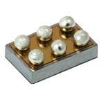
| 产品图片 |
|
| rohs | 符合RoHS无铅 / 符合限制有害物质指令(RoHS)规范要求 |
| 产品系列 | 晶体管,MOSFET,Fairchild Semiconductor FDZ197PZPowerTrench® |
| 数据手册 | |
| 产品型号 | FDZ197PZ |
| Pd-PowerDissipation | 1.9 W |
| Pd-功率耗散 | 1.9 W |
| RdsOn-Drain-SourceResistance | 68 mOhms |
| RdsOn-漏源导通电阻 | 68 mOhms |
| Vds-Drain-SourceBreakdownVoltage | - 20 V |
| Vds-漏源极击穿电压 | - 20 V |
| Vgs-Gate-SourceBreakdownVoltage | +/- 8 V |
| Vgs-栅源极击穿电压 | 8 V |
| 上升时间 | 5.9 ns |
| 下降时间 | 280 ns |
| 不同Id时的Vgs(th)(最大值) | 1V @ 250µA |
| 不同Vds时的输入电容(Ciss) | 1570pF @ 10V |
| 不同Vgs时的栅极电荷(Qg) | 25nC @ 4.5V |
| 不同 Id、Vgs时的 RdsOn(最大值) | 64 毫欧 @ 2A,4.5V |
| 产品种类 | MOSFET |
| 供应商器件封装 | 6-WLCSP |
| 其它名称 | FDZ197PZTR |
| 典型关闭延迟时间 | 311 ns |
| 功率-最大值 | 900mW |
| 包装 | 带卷 (TR) |
| 单位重量 | 54 mg |
| 商标 | Fairchild Semiconductor |
| 安装类型 | 表面贴装 |
| 安装风格 | SMD/SMT |
| 封装 | Reel |
| 封装/外壳 | 6-UFBGA,WLCSP |
| 封装/箱体 | WLCSP-6 1x1.5 Thin |
| 工厂包装数量 | 5000 |
| 晶体管极性 | P-Channel |
| 最大工作温度 | + 150 C |
| 最小工作温度 | - 55 C |
| 标准包装 | 5,000 |
| 正向跨导-最小值 | 21 S |
| 漏源极电压(Vdss) | 20V |
| 电流-连续漏极(Id)(25°C时) | 3.8A (Ta) |
| 系列 | FDZ197PZ |
| 通道模式 | Enhancement |
| 配置 | Single |


- 商务部:美国ITC正式对集成电路等产品启动337调查
- 曝三星4nm工艺存在良率问题 高通将骁龙8 Gen1或转产台积电
- 太阳诱电将投资9.5亿元在常州建新厂生产MLCC 预计2023年完工
- 英特尔发布欧洲新工厂建设计划 深化IDM 2.0 战略
- 台积电先进制程称霸业界 有大客户加持明年业绩稳了
- 达到5530亿美元!SIA预计今年全球半导体销售额将创下新高
- 英特尔拟将自动驾驶子公司Mobileye上市 估值或超500亿美元
- 三星加码芯片和SET,合并消费电子和移动部门,撤换高东真等 CEO
- 三星电子宣布重大人事变动 还合并消费电子和移动部门
- 海关总署:前11个月进口集成电路产品价值2.52万亿元 增长14.8%


PDF Datasheet 数据手册内容提取
Is Now Part of To learn more about ON Semiconductor, please visit our website at www.onsemi.com Please note: As part of the Fairchild Semiconductor integration, some of the Fairchild orderable part numbers will need to change in order to meet ON Semiconductor’s system requirements. Since the ON Semiconductor product management systems do not have the ability to manage part nomenclature that utilizes an underscore (_), the underscore (_) in the Fairchild part numbers will be changed to a dash (-). This document may contain device numbers with an underscore (_). Please check the ON Semiconductor website to verify the updated device numbers. The most current and up-to-date ordering information can be found at www.onsemi.com. Please email any questions regarding the system integration to Fairchild_questions@onsemi.com. ON Semiconductor and the ON Semiconductor logo are trademarks of Semiconductor Components Industries, LLC dba ON Semiconductor or its subsidiaries in the United States and/or other countries. ON Semiconductor owns the rights to a number of patents, trademarks, copyrights, trade secrets, and other intellectual property. A listing of ON Semiconductor’s product/patent coverage may be accessed at www.onsemi.com/site/pdf/Patent-Marking.pdf. ON Semiconductor reserves the right to make changes without further notice to any products herein. ON Semiconductor makes no warranty, representation or guarantee regarding the suitability of its products for any particular purpose, nor does ON Semiconductor assume any liability arising out of the application or use of any product or circuit, and specifically disclaims any and all liability, including without limitation special, consequential or incidental damages. Buyer is responsible for its products and applications using ON Semiconductor products, including compliance with all laws, regulations and safety requirements or standards, regardless of any support or applications information provided by ON Semiconductor. “Typical” parameters which may be provided in ON Semiconductor data sheets and/or specifications can and do vary in different applications and actual performance may vary over time. All operating parameters, including “Typicals” must be validated for each customer application by customer’s technical experts. ON Semiconductor does not convey any license under its patent rights nor the rights of others. ON Semiconductor products are not designed, intended, or authorized for use as a critical component in life support systems or any FDA Class 3 medical devices or medical devices with a same or similar classification in a foreign jurisdiction or any devices intended for implantation in the human body. Should Buyer purchase or use ON Semiconductor products for any such unintended or unauthorized application, Buyer shall indemnify and hold ON Semiconductor and its officers, employees, subsidiaries, affiliates, and distributors harmless against all claims, costs, damages, and expenses, and reasonable attorney fees arising out of, directly or indirectly, any claim of personal injury or death associated with such unintended or unauthorized use, even if such claim alleges that ON Semiconductor was negligent regarding the design or manufacture of the part. ON Semiconductor is an Equal Opportunity/Affirmative Action Employer. This literature is subject to all applicable copyright laws and is not for resale in any manner.
F D Z 1 9 7 December 2014 P FDZ197PZ Z P - P-Channel 1.5 V Specified PowerTrench® Thin WL-CSP MOSFET C h -20 V, -3.8 A, 64 mΩ a n n Features General Description e l (cid:132) Max r = 64 mΩ at V = -4.5 V, I = -2.0 A Designed on Fairchild's advanced 1.5 V PowerTrench® process 1 DS(on) GS D . with state of the art "fine pitch" WLCSP packaging process, the 5 (cid:132) Max rDS(on) = 71 mΩ at VGS = -2.5 V, ID = -2.0 A FDZ197PZ minimizes both PCB space and r . This V DS(on) (cid:132) Max rDS(on) = 79 mΩ at VGS = -1.8 V, ID = -1.0 A advanced WLCSP MOSFET embodies a breakthrough in S packaging technology which enables the device to combine p (cid:132) Max rDS(on) = 95 mΩ at VGS = -1.5 V, ID = -1.0 A excellent thermal transfer characteristics, ultra-low profile ec (cid:132) Occupies only 1.5 mm2 of PCB area.Less than 50% of the packaging, low gate charge, and low rDS(on). if i area of 2 x 2 BGA e Applications d (cid:132) Ultra-thin package: less than 0.65 mm height when mounted P to PCB (cid:132) Battery management o w (cid:132) HBM ESD protection level > 4400V (Note3) (cid:132) Load switch e (cid:132) RoHS Compliant (cid:132) Battery protection rT r e n c PIN1 h ® S T h S G i n D S W L D - C S P M O TOP BOTTOM S F WL-CSP 1x1.5 Thin E T MOSFET Maximum Ratings TA = 25 °C unless otherwise noted Symbol Parameter Ratings Units V Drain to Source Voltage -20 V DS V Gate to Source Voltage ±8 V GS -Continuous T = 25°C (Note 1a) -3.8 I A A D -Pulsed -15 Power Dissipation T = 25°C (Note 1a) 1.9 P A W D Power Dissipation T = 25°C (Note 1b) 0.9 A T , T Operating and Storage Junction Temperature Range -55 to +150 °C J STG Thermal Characteristics R Thermal Resistance, Junction to Ambient (Note 1a) 65 θJA °C/W R Thermal Resistance, Junction to Ambient (Note 1b) 133 θJA Package Marking and Ordering Information Device Marking Device Package Reel Size Tape Width Quantity 7 FDZ197PZ WL-CSP 1x1.5 Thin 7 ” 8 mm 5000 units ©2009 Fairchild Semiconductor Corporation 1 www.fairchildsemi.com FDZ197PZ Rev.C3
Electrical Characteristics F T = 25 °C unless otherwise noted J D Z Symbol Parameter Test Conditions Min Typ Max Units 1 9 Off Characteristics 7 P BV Drain to Source Breakdown Voltage I = -250 µA, V = 0 V -20 V Z DSS D GS ∆BV Breakdown Voltage Temperature P ∆TDJSS Coefficient ID = -250 µA, referenced to 25 °C -10 mV/°C -C I Zero Gate Voltage Drain Current V = -16 V, V = 0 V -1 µA h DSS DS GS a I Gate to Source Leakage Current V = ±8 V, V = 0 V ±10 µA n GSS GS DS n e On Characteristics l 1 V Gate to Source Threshold Voltage V = V , I = -250 µA -0.4 -0.5 -1.0 V . GS(th) GS DS D 5 ∆VGS(th) Gate to Source Threshold Voltage I = -250 µA, referenced to 25 °C 2.7 mV/°C V ∆TJ Temperature Coefficient D S V = -4.5 V, I = -2.0 A 46 64 p GS D e VGS = -2.5 V, ID = -2.0 A 53 71 c i rDS(on) Static Drain to Source On Resistance VGS = -1.8 V, ID = -1.0 A 59 79 mΩ fie VGS = -1.5 V, ID = -1.0 A 68 95 d V = -4.5 V, I = -2.0 A, P TG S=125 °C D 54 84 o J w gFS Forward Transconductance VDD = -5 V, ID = -3.8 A 21 S e r T Dynamic Characteristics r e C Input Capacitance 1180 1570 pF n iss V = -10 V, V = 0 V, c C Output Capacitance DS GS 190 255 pF h oss f = 1 MHz ® Crss Reverse Transfer Capacitance 160 225 pF T h Switching Characteristics i n t Turn-On Delay Time 5.8 12 ns W d(on) tr Rise Time VDD = -10 V, ID = -3.8 A, 5.9 12 ns L- td(off) Turn-Off Delay Time VGS = -4.5 V, RGEN = 6 Ω 311 498 ns C S tf Fall Time 280 448 ns P Qg Total Gate Charge VGS = 0V to -4.5V 18 25 nC M V = -10 V, Q Gate to Source Charge DD 1.5 nC O gs I = -3.8 A Q Gate to Drain “Miller” Charge D 4.7 nC S gd F E Drain-Source Diode Characteristics T V Source to Drain Diode Forward Voltage V = 0 V, I = -1.1 A (Note 2) -0.6 -1.2 V SD GS S t Reverse Recovery Time 194 310 ns rr I = -3.8 A, di/dt = 100 A/µs Q Reverse Recovery Charge F 344 550 nC rr Notes: 1. RθJA is determined with the device mounted on a 1 in2 pad 2 oz copper pad on a 1.5 x 1.5 in. board of FR-4 material. RθJC is guaranteed by design while RθCA is determined by the user's board design. a. 65 °C/W when mounted on b. 133 °C/W when mounted on a a 1 in2 pad of 2 oz copper. minimum pad of 2 oz copper. 2. Pulse Test: Pulse Width < 300µs, Duty cycle < 2.0%. 3. The diode connected between the gate and source serves only as protection ESD. No gate overvoltage rating is implied. ©2009 Fairchild Semiconductor Corporation 2 www.fairchildsemi.com FDZ197PZ Rev.C3
F D T ypical Characteristics T = 25 °C unless otherwise noted Z J 1 9 7 15 2.5 P E Z , -IDRAIN CURRENT (A) D 1203690 VGSV =G S-V1 G=1.5 S- V 1V=.G 8-SV2 VG.=5S - V3= PDV-4UU.L5T SYVE C DY2UCRLEA T=I O0.N5 %= 8M0A µXs 3 NORMALIZEDDRAIN TO SOURCE ON-RESISTANC 0112....50500 PDUULTVSYGE CS DY=3UC -R1L.EA5 T =VI O0.NV5 G%=S 6 8 M=0 A -µ3Xs VVGS =9 -1.8 VVGSV =G 1S-42 =.5 - 2V.5 V 15 P-Channel 1.5 V Spec -VDS, DRAIN TO SO URCE VOLTAGE (V) -ID, DRAIN CURRENT (A) if i e Figure 1. On-Region Characteristics Figure 2. Normalized On-Resistance d vs Drain Current and Gate Voltage P o w 1.4 150 e ANCE IVDG =S -=2 -A4.5 V )mΩ ID = -2 A PDUULTSYE C DYUCRLEA T=I O0.N5 %= 8M0A µXs rTre NORMALIZED O SOURCE ON-RESIST 011...802 rDRAIN TO ,DS(on)(CE ON-RESISTANCE 1269000 TJ = 125 oC nch ThinW® RAIN T SOUR TJ = 25 oC L-C D 0.6 30 S -75 -50 -25 0 25 50 75 100 125 150 1.0 1.5 2.0 2.5 3.0 3.5 4.0 4.5 P TJ, JUNCTION TEM PERATURE (oC) -VGS, GATE TO SOURCE VOLTAGE (V) M O Figure 3. Normalized On- Resistance Figure 4. On-Resistance vs Gate to S vs Junction Temperature Source Voltage F E T 15 20 PULSE DURATION = 80 µs A) 10 VGS = 0 V DUTY CYCLE = 0.5% MAX T ( 12 N E RRENT (A) 9 VDS = -5 V AIN CURR 1 TJ = 150 oC CU DR 0.1 TJ = 25 oC N 6 E RAI TJ = 150 oC TJ = 25 oC ERS -I, DD 3 TJ = -55 oC -I, REVS0.01 TJ = -55 oC 0 0.001 0.0 0.5 1.0 1.5 2.0 0.0 0.2 0.4 0.6 0.8 1.0 1.2 -VGS, GATE TO SO URCE VOLTAGE (V) -VSD, BODY DIODE FO RWARD VOLTAGE (V) Figure 5. Transfer Characteristics Figure 6. Source to Drain Diode Forward Voltage vs Source Current ©2009 Fairchild Semiconductor Corporation 3 www.fairchildsemi.com FDZ197PZ Rev.C3
F D Typical Characteristics T = 25 °C unless otherwise noted Z J 1 9 7 4.5 3000 P VOLTAGE (V)3.0 ID = -3.8 A VDD = -8 V CE (pF)1000 Ciss Z P-Ch RCE VDD = -10 V TAN an U CI n TO SO1.5 VDD = -12 V CAPA Coss el 1 E . T 5 A G V V, GS fV =G S1 =M 0H Vz Crss S -0.0 100 p 0 3 6 9 12 15 18 0.1 1 10 20 e c Qg, GATE CH ARGE (nC) -VDS, DRAIN TO SOU RCE VOLTAGE (V) i f i e Figure 7. Gate Charge Characteristics Figure 8. Capacitance vs Drain d to Source Voltage P o w 10 20 e 10 r T A) 100 µs r RENT ( NT (A) 1 ms enc ANCHE CUR 1 TJ = 125 oC TJ = 25 oC RAIN CURRE 1 TLIHMISIT AERDE BAY I SrD S(on) 1100 0m mss h Thin® -I, AVALAS -I, DD 0.1 STRTJAIθN J ==AG M2=L5 AE1 Xo 3PC 3RU oALCST/WEED 1D sC WL-C 0.1 0.01 S 0.01 0.1 1 10 100 1000 0.1 1 10 50 P tAV, TIME IN AVA LANCHE (ms) -VDS, DRAIN to SOU RCE VOLTAGE (V) M O Figure 9. Unclamped Inductive Figure 10. Forward Bias Safe S Switching Capability Operating Area F E T 10-2 200 NT (A) 10-3 VGS = 0 V WER (W) 100 SRIθNJAG =L E1 3P3U oLCS/WE URRE 10-4 T PO TA = 25 oC ATE LEAKAGE C 111000---765 TJ = 125 oC TJ = 25 oC PEAK TRANSIEN 10 , -IGg 10-8 , P()PK 1 10-9 0.5 0 3 6 9 12 15 10-4 10-3 10-2 10-1 1 10 100 1000 -VGS, GATE TO SOURCE VOLTAGE (V) t, PULSE WIDTH (sec) Figure 11. Gate Leakage Current vs Figure 12. Single Pulse Maximum Gate to Source Voltage Power Dissipation ©2009 Fairchild Semiconductor Corporation 4 www.fairchildsemi.com FDZ197PZ Rev.C3
F Typical Characteristics D T = 25 °C unless otherwise noted J Z 1 9 7 2 P 1 DUTY CYCLE-DESCENDING ORDER Z P D = 0.5 AL 0.2 -C M A 0.1 h ERZJθ 0.05 a ORMALIZED TH IMPEDANCE, 0.1 00..0021 PDM t1t2 nnel 1.5 N SINGLE PULSE NOTES: V 0.01 RθJA = 133 oC/W DPEUATYK FTAJ C= TPODRM: xD Z =θ JtA1 /xt2 RθJA + TA Sp e 0.005 c 10-4 10-3 10-2 10-1 1 10 100 1000 i f t, RECTANGULAR PULSE DURATION (sec) ie d Figure 13. Transient Thermal Response Curve P o w e r T r e n c h ® T h i n W L - C S P M O S F E T ©2009 Fairchild Semiconductor Corporation 5 www.fairchildsemi.com FDZ197PZ Rev.C3
F D Z Dimensional Outline and Pad Layout 1 9 7 P Z P - C h a n n e l 1 . 5 V S p e c i f i e d P o w e r T r e n c h ® T h i n W L - C S P M O S F E T Pin Definations: Gate Drain Source A1 C1, C2 A2, B1, B2 Package drawings are provided as a service to customers considering Fairchild components. Drawings may change in any manner without notice. Please note the revision and/or date on the drawing and contact a Fairchild Semiconductor representative to verify or obtain the most recent revision. Package specifications do not expand the terms of Fairchild's worldwide terms and conditions, specifically the warranty therein, which covers Fairchild products. Always visit Fairchild Semiconductor’s online packaging area for the most recent package drawings: http://www.fairchildsemi.com/package/packageDetails.html?id=PN_UCBAU-006 ©2009 Fairchild Semiconductor Corporation www.fairchildsemi.com FDZ197PZ Rev.C3
F D Z 1 9 7 P TRADEMARKS Z The following includes registered and unregistered trademarks and service marks, owned by Fairchild Semiconductor and/or its global subsidiaries, and is not intended to be an exhaustive list of all such trademarks. P - AccuPower F-PFS OPTOPLANAR® C AttitudeEngine™ FRFET® ®* h Awinda® Global Power ResourceSM ® TinyBoost® a AX-CAP®* GreenBridge PowerTrench® TinyBuck® nn BitSiC Green FPS PowerXS™ TinyCalc e Build it Now Green FPS e-Series Programmable Active Droop TinyLogic® l CorePLUS Gmax QFET® TINYOPTO 1 . CorePOWER GTO QS TinyPower 5 CROSSVOLT IntelliMAX Quiet Series TinyPWM V CTL ISOPLANAR RapidConfigure TinyWire S DDCuEuarUrle XCnPto EoTElr™aDn ®s fer Logic MMeagkiaannBgdu S cBmkeatt lel rS™pe akers Sound Louder Saving our world, 1mW/W/kW at a time™ TTTRrriaFUnaESuCilCt UDRe RteEcNtT ®* pec EEcffoicSiePnAtMRaKx® MMIicCrRoFOECTOU PLER SSmignaartlMWaisxe μSerDes ifie FEaSiBrcCh®i ld ® MMMiiiccllerroorDPPraaikkve2 SSSSMToPlEMuAAtR®ioL TnT sHS fToAr RYTour Success UUHltrCa ®F RFE T d Po Fairchild Semiconductor® MotionMax SuperFET® UniFET w MotionGrid® VCX e FFFFFAEaAAsCTCStBTvTTC®e® Q nocurehiet Series mMMMTTVWxiN®S®® a ver® SSSSSuuyuunppppecreeerFrrSMSSEOOOTOTTTS ®- 3--86 XVVXsioSsel™utnaasg l™MeP alxus rTrenc FPS OOPptToOHLiTOG IC® Sync-Lock™ 仙童™ h® * Trademarks of System General Corporation, used under license by Fairchild Semiconductor. T h DISCLAIMER i n FAIRCHILD SEMICONDUCTOR RESERVES THE RIGHT TO MAKE CHANGES WITHOUT FURTHER NOTICE TO ANY PRODUCTS HEREIN TO IMPROVE RELIABILITY, FUNCTION, OR DESIGN. TO OBTAIN THE LATEST, MOST UP-TO-DATE DATASHEET AND PRODUCT INFORMATION, VISIT OUR WEBSITE W AT HTTP://WWW.FAIRCHILDSEMI.COM. FAIRCHILD DOES NOT ASSUME ANY LIABILITY ARISING OUT OF THE APPLICATION OR USE OF ANY L PRODUCT OR CIRCUIT DESCRIBED HEREIN; NEITHER DOES IT CONVEY ANY LICENSE UNDER ITS PATENT RIGHTS, NOR THE RIGHTS OF OTHERS. - C THESE SPECIFICATIONS DO NOT EXPAND THE TERMS OF FAIRCHILD’S WORLDWIDE TERMS AND CONDITIONS, SPECIFICALLY THE WARRANTY S THEREIN, WHICH COVERS THESE PRODUCTS. P LIFE SUPPORT POLICY M FAIRCHILD’S PRODUCTS ARE NOT AUTHORIZED FOR USE AS CRITICAL COMPONENTS IN LIFE SUPPORT DEVICES OR SYSTEMS WITHOUT THE O EXPRESS WRITTEN APPROVAL OF FAIRCHILD SEMICONDUCTOR CORPORATION. S As used herein: F 1. Life support devices or systems are devices or systems which, (a) are 2. A critical component in any component of a life support, device, or E intended for surgical implant into the body or (b) support or sustain system whose failure to perform can be reasonably expected to T life, and (c) whose failure to perform when properly used in cause the failure of the life support device or system, or to affect its accordance with instructions for use provided in the labeling, can be safety or effectiveness. reasonably expected to result in a significant injury of the user. ANTI-COUNTERFEITING POLICY Fairchild Semiconductor Corporation's Anti-Counterfeiting Policy. Fairchild's Anti-Counterfeiting Policy is also stated on our external website, www.fairchildsemi.com, under Sales Support. . Counterfeiting of semiconductor parts is a growing problem in the industry. All manufacturers of semiconductor products are experiencing counterfeiting of their parts. Customers who inadvertently purchase counterfeit parts experience many problems such as loss of brand reputation, substandard performance, failed applications, and increased cost of production and manufacturing delays. Fairchild is taking strong measures to protect ourselves and our customers from the proliferation of counterfeit parts. Fairchild strongly encourages customers to purchase Fairchild parts either directly from Fairchild or from Authorized Fairchild Distributors who are listed by country on our web page cited above. Products customers buy either from Fairchild directly or from Authorized Fairchild Distributors are genuine parts, have full traceability, meet Fairchild's quality standards for handling and storage and provide access to Fairchild's full range of up-to-date technical and product information. Fairchild and our Authorized Distributors will stand behind all warranties and will appropriately address any warranty issues that may arise. Fairchild will not provide any warranty coverage or other assistance for parts bought from Unauthorized Sources. Fairchild is committed to combat this global problem and encourage our customers to do their part in stopping this practice by buying direct or from authorized distributors. PRODUCT STATUS DEFINITIONS Definition of Terms Datasheet Identification Product Status Definition Datasheet contains the design specifications for product development. Specifications may change Advance Information Formative / In Design in any manner without notice. Datasheet contains preliminary data; supplementary data will be published at a later date. Fairchild Preliminary First Production Semiconductor reserves the right to make changes at any time without notice to improve design. Datasheet contains final specifications. Fairchild Semiconductor reserves the right to make No Identification Needed Full Production changes at any time without notice to improve the design. Datasheet contains specifications on a product that is discontinued by Fairchild Semiconductor. Obsolete Not In Production The datasheet is for reference information only. Rev. I73 FDZ197PZ Rev.C3 www.fairchildsemi.com
ON Semiconductor and are trademarks of Semiconductor Components Industries, LLC dba ON Semiconductor or its subsidiaries in the United States and/or other countries. ON Semiconductor owns the rights to a number of patents, trademarks, copyrights, trade secrets, and other intellectual property. A listing of ON Semiconductor’s product/patent coverage may be accessed at www.onsemi.com/site/pdf/Patent−Marking.pdf. ON Semiconductor reserves the right to make changes without further notice to any products herein. ON Semiconductor makes no warranty, representation or guarantee regarding the suitability of its products for any particular purpose, nor does ON Semiconductor assume any liability arising out of the application or use of any product or circuit, and specifically disclaims any and all liability, including without limitation special, consequential or incidental damages. Buyer is responsible for its products and applications using ON Semiconductor products, including compliance with all laws, regulations and safety requirements or standards, regardless of any support or applications information provided by ON Semiconductor. “Typical” parameters which may be provided in ON Semiconductor data sheets and/or specifications can and do vary in different applications and actual performance may vary over time. All operating parameters, including “Typicals” must be validated for each customer application by customer’s technical experts. ON Semiconductor does not convey any license under its patent rights nor the rights of others. ON Semiconductor products are not designed, intended, or authorized for use as a critical component in life support systems or any FDA Class 3 medical devices or medical devices with a same or similar classification in a foreign jurisdiction or any devices intended for implantation in the human body. Should Buyer purchase or use ON Semiconductor products for any such unintended or unauthorized application, Buyer shall indemnify and hold ON Semiconductor and its officers, employees, subsidiaries, affiliates, and distributors harmless against all claims, costs, damages, and expenses, and reasonable attorney fees arising out of, directly or indirectly, any claim of personal injury or death associated with such unintended or unauthorized use, even if such claim alleges that ON Semiconductor was negligent regarding the design or manufacture of the part. ON Semiconductor is an Equal Opportunity/Affirmative Action Employer. This literature is subject to all applicable copyright laws and is not for resale in any manner. PUBLICATION ORDERING INFORMATION LITERATURE FULFILLMENT: N. American Technical Support: 800−282−9855 Toll Free ON Semiconductor Website: www.onsemi.com Literature Distribution Center for ON Semiconductor USA/Canada 19521 E. 32nd Pkwy, Aurora, Colorado 80011 USA Europe, Middle East and Africa Technical Support: Order Literature: http://www.onsemi.com/orderlit Phone: 303−675−2175 or 800−344−3860 Toll Free USA/Canada Phone: 421 33 790 2910 Fax: 303−675−2176 or 800−344−3867 Toll Free USA/Canada Japan Customer Focus Center For additional information, please contact your local Email: orderlit@onsemi.com Phone: 81−3−5817−1050 Sales Representative © Semiconductor Components Industries, LLC www.onsemi.com www.onsemi.com 1
Mouser Electronics Authorized Distributor Click to View Pricing, Inventory, Delivery & Lifecycle Information: O N Semiconductor: FDZ197PZ