ICGOO在线商城 > 分立半导体产品 > 晶体管 - FET,MOSFET - 单 > DMN53D0LW-7
 Datasheet下载
- 型号: DMN53D0LW-7
- 制造商: Diodes Inc.
- 库位|库存: xxxx|xxxx
- 要求:
| 数量阶梯 | 香港交货 | 国内含税 |
| +xxxx | $xxxx | ¥xxxx |
查看当月历史价格
查看今年历史价格
DMN53D0LW-7产品简介:
ICGOO电子元器件商城为您提供DMN53D0LW-7由Diodes Inc.设计生产,在icgoo商城现货销售,并且可以通过原厂、代理商等渠道进行代购。 DMN53D0LW-7价格参考。Diodes Inc.DMN53D0LW-7封装/规格:晶体管 - FET,MOSFET - 单, 表面贴装 N 沟道 50V 360mA(Ta) 320mW(Ta) SOT-323。您可以下载DMN53D0LW-7参考资料、Datasheet数据手册功能说明书,资料中有DMN53D0LW-7 详细功能的应用电路图电压和使用方法及教程。
DMN53D0LW-7 是由 Diodes Incorporated 生产的一款 N 沟道增强型 MOSFET,属于晶体管 - FET、MOSFET - 单类别。该型号具有低导通电阻(Rds(on))和快速开关特性,适用于多种电力电子应用场景。以下是其主要应用场景:

1. 电源管理:
   DMN53D0LW-7 常用于 DC-DC 转换器、降压/升压转换器以及负载开关等电路中,提供高效的功率传输和低损耗性能。它的低 Rds(on) 可以减少导通时的功耗,适合便携式设备和电池供电系统。

2. 电机驱动:
   该 MOSFET 可用于小型直流电机或步进电机的驱动电路中,支持高频率 PWM 控制,实现精确的速度调节和方向控制。

3. 保护电路:
   在过流保护、短路保护和电子保险丝应用中,DMN53D0LW-7 的快速开关特性和低导通电阻使其成为理想选择,能够有效限制异常电流并保护下游电路。

4. 音频放大器:
   作为音频信号放大器中的功率级元件,DMN53D0LW-7 可以提供高效且线性良好的输出驱动能力,同时降低热损耗。

5. 消费电子产品:
   广泛应用于智能手机、平板电脑、笔记本电脑和其他消费类电子产品中,用于充电管理、背光驱动和信号切换等功能。

6. 工业自动化:
   在工业控制系统中,可用于信号隔离、传感器接口和继电器替代等场合,提供可靠的开关功能。

总结来说,DMN53D0LW-7 凭借其优异的电气特性和紧凑的封装形式(如 WDFN-8),非常适合需要高效、低功耗和小尺寸解决方案的应用领域。
| 参数 | 数值 |
| 产品目录 | |
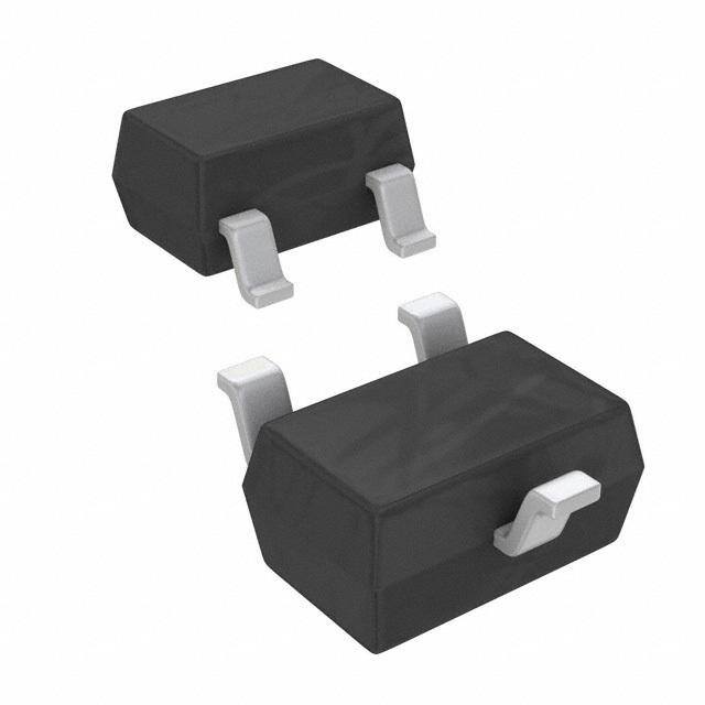
| 描述 | MOSFET N-CH 50V 360MA SOT323 |
| 产品分类 | FET - 单 |
| FET功能 | 逻辑电平门 |
| FET类型 | MOSFET N 通道,金属氧化物 |
| 品牌 | Diodes Incorporated |
| 数据手册 | |
| 产品图片 |
|
| 产品型号 | DMN53D0LW-7 |
| rohs | 无铅 / 符合限制有害物质指令(RoHS)规范要求 |
| RoHS指令信息 | http://diodes.com/download/4349 |
| 产品系列 | - |
| 不同Id时的Vgs(th)(最大值) | 1.5V @ 100µA |
| 不同Vds时的输入电容(Ciss) | 45.8pF @ 25V |
| 不同Vgs时的栅极电荷(Qg) | 1.2nC @ 10V |
| 不同 Id、Vgs时的 RdsOn(最大值) | 2 欧姆 @ 270mA,10V |
| 供应商器件封装 | SOT-323 |
| 其它名称 | DMN53D0LW-7DIDKR |
| 功率-最大值 | 320mW |
| 包装 | Digi-Reel® |
| 安装类型 | 表面贴装 |
| 封装/外壳 | SC-70,SOT-323 |
| 标准包装 | 1 |
| 漏源极电压(Vdss) | 50V |
| 电流-连续漏极(Id)(25°C时) | 360mA (Ta) |


PDF Datasheet 数据手册内容提取
DMN53D0LW N-CHANNEL ENHANCEMENT MODE MOSFET Product Summary Features ID N-Channel MOSFET V(BR)DSS RDS(ON) TA = +25°C Low On-Resistance 2.0Ω @ VGS = 10V 360mA Low Input Capacitance 50V 3.0Ω @ VGS = 5V 250mA Fast Switching Speed T ESD Protected Gate C Description Totally Lead-Free & Fully RoHS Compliant (Notes 1 & 2) U Halogen and Antimony Free. “Green” Device (Note 3) D This new generation MOSFET has been designed to minimize the Qualified to AEC-Q101 Standards for High Reliability O on-state resistance (RDS(ON)) and yet maintain superior switching R performance, making it ideal for high efficiency power management Mechanical Data P applications. W Case: SOT323 E Applications Case Material: Molded Plastic. UL Flammability Classification N Rating 94V-0 DC-DC Converters Moisture Sensitivity: Level 1 per J-STD-020 Power management functions Terminals: Matte Tin Finish annealed over Alloy 42 leadframe Battery Operated Systems and Solid-State Relays (Lead Free Plating). Solderable per MIL-STD-202, Method 208 e3 Drivers: Relays, Solenoids, Lamps, Hammers, Displays, Terminal Connections: See Diagram Memories, Transistors, etc Weight: 0.006 grams (approximate) Drain SOT323 D Gate G S Gate Protection Source ESD PROTECTED Diode Top View Top View Pin Configuration Equivalent Circuit Ordering Information (Note 4) Part Number Case Packaging DMN53D0LW-7 SOT323 3,000/Tape & Reel DMN53D0LW-13 SOT323 10,000/Tape & Reel Notes: 1. No purposely added lead. Fully EU Directive 2002/95/EC (RoHS) & 2011/65/EU (RoHS 2) compliant. 2. See http://www.diodes.com/quality/lead_free.html for more information about Diodes Incorporated’s definitions of Halogen- and Antimony-free, "Green" and Lead-free. 3. Halogen- and Antimony-free "Green” products are defined as those which contain <900ppm bromine, <900ppm chlorine (<1500ppm total Br + Cl) and <1000ppm antimony compounds. 4. For packaging details, go to our website at http://www.diodes.com/products/packages.html. Marking Information MM5 = Product Type Marking Code YM = Date Code Marking for SAT (Shanghai Assembly/ Test site) Y = Year (ex: A = 2013) M = Month (ex: 9 = September) Shanghai A/T Site Date Code Key Year 2011 2012 2013 2014 2015 2016 2017 Code Y Z A B C D E Month Jan Feb Mar Apr May Jun Jul Aug Sep Oct Nov Dec Code 1 2 3 4 5 6 7 8 9 O N D DMN53D0LW 1 of 5 November 2013 Document number: DS36579 Rev. 2 - 2 www.diodes.com © Diodes Incorporated
DMN53D0LW Maximum Ratings (@TA = +25°C, unless otherwise specified.) Characteristic Symbol Value Units Drain-Source Voltage VDSS 50 V Gate-Source Voltage VGSS ±20 V Continuous Drain Current (Note 6) VGS = 10V SStetaatdey TTAA == ++2750°°CC ID 326500 mA T UC Continuous Drain Current (Note 6) VGS = 5V SStetaatdey TTAA == ++2750°°CC ID 225000 mA D Pulsed Drain Current (10µs pulse, duty cycle = 1%) IDM 700 mA O R P W Thermal Characteristics (@TA = +25°C, unless otherwise specified.) E Characteristic Symbol Value Units N (Note 5) 320 Total Power Dissipation (Note 6) PD 420 mW (Note 5) 395 Thermal Resistance, Junction to Ambient (Note 6) RθJA 301 °C/W Operating and Storage Temperature Range TJ, TSTG -55 to 150 °C Electrical Characteristics (@TA = +25°C, unless otherwise specified.) Characteristic Symbol Min Typ Max Unit Test Condition OFF CHARACTERISTICS (Note 7) Drain-Source Breakdown Voltage BVDSS 50 V VGS = 0V, ID = 250µA Zero Gate Voltage Drain Current IDSS 1.0 µA VDS = 50V, VGS = 0V Gate-Body Leakage IGSS ±10 µA VGS = ±12V, VDS = 0V ON CHARACTERISTICS (Note 7) Gate Threshold Voltage VGS(TH) 0.8 1.5 V VDS = VGS, ID = 100µA V GS(TH) Gate Threshold Voltage Temperature Coefficient (Note 8) -3.4 mV/°C — T J 2.0 VGS = 10V, ID = 270mA Static Drain-Source On-Resistance RDS (ON) Ω 3.0 VGS = 5V, ID = 200mA Forward Transconductance gFS 80 mS VDS = 10V, ID = 200mA Diode Forward Voltage VSD — 0.75 1.2 V VGS = 0V, IS = 115mA DYNAMIC CHARACTERISTICS (Note 8) Input Capacitance Ciss 45.8 Output Capacitance Coss 5.3 pF fV =D S1 =.0 2M5HVz, VGS = 0V Reverse Transfer Capacitance Crss 3.9 Total Gate Charge VGS = 10V Qg 1.2 Total Gate Charge VGS = 4.5V Qg 0.6 nC VGS = 10V, VDS = 10V, Gate-Source Charge Qgs 0.2 ID = 250mA Gate-Drain Charge Qgd 0.1 Turn-On Delay Time tD(on) 2.7 Turn-On Rise Time tr 2.5 nS VDD = 30V, VGS = 10V, Turn-Off Delay Time tD(off) 18.9 RG = 25Ω, ID = 200mA Turn-Off Fall Time tf 11.0 Notes: 5. Device mounted on FR-4 PC board, with minimum recommended pad layout, single sided. 6. Device mounted on FR-4 substrate PC board, 2oz copper, with 1inch square copper pad layout 7 .Short duration pulse test used to minimize self-heating effect. 8. Guaranteed by design. Not subject to production testing. DMN53D0LW 2 of 5 November 2013 Document number: DS36579 Rev. 2 - 2 www.diodes.com © Diodes Incorporated
DMN53D0LW 1.5 1 VGS = 10V VGS = 3V VDS = 5V 1.2 0.8 A) VGS = 5V A) T ( T ( N N E 0.9 E0.6 T RR VGS = 4.5V RR C CU VGS = 2.5V CU U AIN 0.6 VGS = 3.5V AIN 0.4 TA = 150°C D R R D D PRO I, D0.3 VGS = 2V VGS = 1.8V I, D0.2 TA = 125°C TAT A= =2 58°5C°C W E TA = -55°C 0.0 0 N 0 1 2 3 4 5 0 0.5 1 1.5 2 2.5 3 3.5 4 4.5 5 VDS, DRAIN-SOURCE VOLTAGE (V) VGS, GATE-SOURCE VOLTAGE (V) Figure 1 Typical Output Characteristics Figure 2 Typical Transfer Characteristics 1 2.5 ) ) E ( E ( VGS = 4.5V C C N N A 0.9 A 2 T T ESIS VGS = 5V ESIS TA = 150°C R R ON- 0.8 VGS = 10V ON- 1.5 TA = 125°C E E RC RC TA = 85°C U 0.7 U 1 O O S S N- N- TA = 25°C AI AI R R D 0.6 D 0.5 , N) , N) TA = -55°C O O S( S( D D R 0.5 R 0 0 0.2 0.4 0.6 0.8 1 0 0.2 0.4 0.6 0.8 1 I , DRAIN-SOURCE CURRENT (A) I , DRAIN CURRENT (A) D D Figure 3 Typical On-Resistance vs. Figure 4 Typical On-Resistance vs. Drain Current and Gate Voltage Drain Current and Temperature 2.4 2 ) E ( 1.8 C D) 2.0 AN 1.6 RCE ALIZE IVDG =S 5 =0 01m0VA ESIST 1.4 VGS = 5V OURM 1.6 N-R 1.2 ID = 300mA SO O AIN-E (N VGS = 5V CE 1 , DRDS(ON)ESISTANC 1.2 ID = 300mA AIN-SOUR 00..68 IVDG =S 5 =0 01m0VA RR R ON- 0.8 , DN) 0.4 O 0.2 S( D R 0.4 0 -50 -25 0 25 50 75 100 125 150 -50 -25 0 25 50 75 100 125 150 TJ, JUNCTION TEMPERATURE (C) TJ, JUNCTION TEMPERATURE (C) Figure 5 On-Resistance Variation with Temperature Figure 6 On-Resistance Variation with Temperature DMN53D0LW 3 of 5 November 2013 Document number: DS36579 Rev. 2 - 2 www.diodes.com © Diodes Incorporated
DMN53D0LW 2.0 1.0 V) E ( 1.8 G 0.8 A CT SHOLD VOLT 11..46 ID = 1mA CURRENT (A) 0.6 TA = T1A2 5=° C150°C U HRE 1.2 ID = 250µA CE 0.4 OD ATE T 1.0 SOUR TA = 85°C TA = 25°C PR , Gh) I, S0.2 W VGS(t 0.8 TA = -55°C E 0.6 0 N -50 -25 0 25 50 75 100 125 150 0 0.3 0.6 0.9 1.2 1.5 T, JUNCTION TEMPERATURE (C) J V , SOURCE-DRAIN VOLTAGE (V) SD Figure 7 Gate Threshold Variation vs. Ambient Temperature Figure 8 Diode Forward Voltage vs. Current 100 10 Ciss V) pF) E ( 8 E ( AG C T N L A O CIT D V 6 APA10 HOL VIDD =S 2=5 100mVA C S TION Coss THRE 4 NC TE C, JUT Crss GAGS 2 V f = 1MHz 1 0 0 5 10 15 20 25 30 35 40 0 0.3 0.6 0.9 1.2 1.5 VDS, DRAIN-SOURCE VOLTAGE (V) Qg, TOTAL GATE CHARGE (nC) Figure 9 Typical Junction Capacitance Figure 10 Gate Charge Package Outline Dimensions Please see AP02002 at http://www.diodes.com/datasheets/ap02002.pdf for the latest version. SOT323 A Dim Min Max Typ A 0.25 0.40 0.30 B 1.15 1.35 1.30 B C C 2.00 2.20 2.10 D - - 0.65 G 1.20 1.40 1.30 G H 1.80 2.20 2.15 H J 0.0 0.10 0.05 K 0.90 1.00 1.00 K M L 0.25 0.40 0.30 M 0.10 0.18 0.11 0° 8° - J D L All Dimensions in mm DMN53D0LW 4 of 5 November 2013 Document number: DS36579 Rev. 2 - 2 www.diodes.com © Diodes Incorporated
DMN53D0LW Suggested Pad Layout Please see AP02001 at http://www.diodes.com/datasheets/ap02001.pdf for the latest version. Y Dimensions Value (in mm) Z 2.8 T C Z C X 0.7 Y 0.9 U C 1.9 D E 1.0 O R P X E W E N IMPORTANT NOTICE DIODES INCORPORATED MAKES NO WARRANTY OF ANY KIND, EXPRESS OR IMPLIED, WITH REGARDS TO THIS DOCUMENT, INCLUDING, BUT NOT LIMITED TO, THE IMPLIED WARRANTIES OF MERCHANTABILITY AND FITNESS FOR A PARTICULAR PURPOSE (AND THEIR EQUIVALENTS UNDER THE LAWS OF ANY JURISDICTION). Diodes Incorporated and its subsidiaries reserve the right to make modifications, enhancements, improvements, corrections or other changes without further notice to this document and any product described herein. Diodes Incorporated does not assume any liability arising out of the application or use of this document or any product described herein; neither does Diodes Incorporated convey any license under its patent or trademark rights, nor the rights of others. Any Customer or user of this document or products described herein in such applications shall assume all risks of such use and will agree to hold Diodes Incorporated and all the companies whose products are represented on Diodes Incorporated website, harmless against all damages. Diodes Incorporated does not warrant or accept any liability whatsoever in respect of any products purchased through unauthorized sales channel. Should Customers purchase or use Diodes Incorporated products for any unintended or unauthorized application, Customers shall indemnify and hold Diodes Incorporated and its representatives harmless against all claims, damages, expenses, and attorney fees arising out of, directly or indirectly, any claim of personal injury or death associated with such unintended or unauthorized application. Products described herein may be covered by one or more United States, international or foreign patents pending. Product names and markings noted herein may also be covered by one or more United States, international or foreign trademarks. This document is written in English but may be translated into multiple languages for reference. Only the English version of this document is the final and determinative format released by Diodes Incorporated. LIFE SUPPORT Diodes Incorporated products are specifically not authorized for use as critical components in life support devices or systems without the express written approval of the Chief Executive Officer of Diodes Incorporated. As used herein: A. Life support devices or systems are devices or systems which: 1. are intended to implant into the body, or 2. support or sustain life and whose failure to perform when properly used in accordance with instructions for use provided in the labeling can be reasonably expected to result in significant injury to the user. B. A critical component is any component in a life support device or system whose failure to perform can be reasonably expected to cause the failure of the life support device or to affect its safety or effectiveness. Customers represent that they have all necessary expertise in the safety and regulatory ramifications of their life support devices or systems, and acknowledge and agree that they are solely responsible for all legal, regulatory and safety-related requirements concerning their products and any use of Diodes Incorporated products in such safety-critical, life support devices or systems, notwithstanding any devices- or systems-related information or support that may be provided by Diodes Incorporated. Further, Customers must fully indemnify Diodes Incorporated and its representatives against any damages arising out of the use of Diodes Incorporated products in such safety-critical, life support devices or systems. Copyright © 2013, Diodes Incorporated www.diodes.com DMN53D0LW 5 of 5 November 2013 Document number: DS36579 Rev. 2 - 2 www.diodes.com © Diodes Incorporated