ICGOO在线商城 > 分立半导体产品 > 晶体管 - FET,MOSFET - 单 > STD10P6F6
 Datasheet下载
- 型号: STD10P6F6
- 制造商: STMicroelectronics
- 库位|库存: xxxx|xxxx
- 要求:
| 数量阶梯 | 香港交货 | 国内含税 |
| +xxxx | $xxxx | ¥xxxx |
查看当月历史价格
查看今年历史价格
STD10P6F6产品简介:
ICGOO电子元器件商城为您提供STD10P6F6由STMicroelectronics设计生产,在icgoo商城现货销售,并且可以通过原厂、代理商等渠道进行代购。 STD10P6F6价格参考。STMicroelectronicsSTD10P6F6封装/规格:晶体管 - FET,MOSFET - 单, P-Channel 60V 10A (Tc) 35W (Tc) Surface Mount DPAK。您可以下载STD10P6F6参考资料、Datasheet数据手册功能说明书,资料中有STD10P6F6 详细功能的应用电路图电压和使用方法及教程。
STMicroelectronics(意法半导体)的STD10P6F6是一款P沟道增强型MOSFET,属于晶体管中的场效应管(FET),常用于电源管理和开关控制应用。该器件具有100V耐压、连续漏极电流达10A,导通电阻低,适用于高效率、低功耗的设计场景。

典型应用场景包括:

1. 电源开关电路:常用于DC-DC转换器、负载开关或电源管理模块中,作为高端或低端开关,实现对电源通断的高效控制。

2. 电池供电设备:由于其低导通损耗和良好热性能,适合应用于便携式设备如笔记本电脑、移动电源、电动工具等,用于电池充放电管理和反向电流保护。

3. 电机驱动:在中小功率直流电机或步进电机驱动电路中,作为开关元件参与H桥或半桥拓扑结构,控制电机启停与方向。

4. 逆变器与UPS系统:用于不间断电源(UPS)、逆变器等工业电源系统中,承担功率切换与能量传输功能。

5. 过压/过流保护电路:可配合控制芯片实现输入电源的热插拔保护或防反接设计,提高系统可靠性。

6. 工业控制与汽车电子:因其具备良好的温度稳定性和抗干扰能力,也适用于工业自动化设备及车载辅助电源系统。

综上,STD10P6F6凭借其高电压耐受、大电流能力和高可靠性,广泛应用于消费电子、工业控制、汽车电子及电源管理系统中,尤其适合需要高效开关和紧凑设计的场合。
| 参数 | 数值 |
| 产品目录 | |
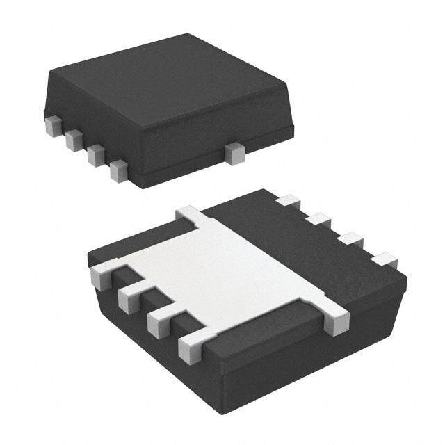
| 描述 | MOSFET P CH 60V 10A DPAKMOSFET P-Ch 60V 0.15Ohm 10A STripFET VI DeepGate |
| 产品分类 | FET - 单分离式半导体 |
| FET功能 | 标准 |
| FET类型 | MOSFET P 通道,金属氧化物 |
| Id-ContinuousDrainCurrent | 10 A |
| Id-连续漏极电流 | 10 A |
| 品牌 | STMicroelectronics |
| 产品手册 | |
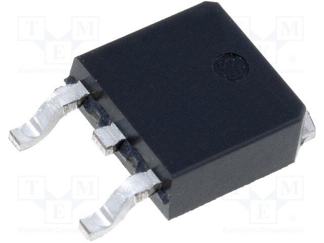
| 产品图片 |
|
| rohs | 符合RoHS无铅 / 符合限制有害物质指令(RoHS)规范要求 |
| 产品系列 | 晶体管,MOSFET,STMicroelectronics STD10P6F6DeepGATE™, STripFET™ VI |
| 数据手册 | |
| 产品型号 | STD10P6F6 |
| Pd-PowerDissipation | 35 W |
| Pd-功率耗散 | 35 W |
| Qg-GateCharge | 7 nC |
| Qg-栅极电荷 | 7 nC |
| RdsOn-Drain-SourceResistance | 180 mOhms |
| RdsOn-漏源导通电阻 | 180 mOhms |
| Vds-Drain-SourceBreakdownVoltage | 60 V |
| Vds-漏源极击穿电压 | - 60 V |
| Vgs-Gate-SourceBreakdownVoltage | 20 V |
| Vgs-栅源极击穿电压 | 20 V |
| Vgsth-Gate-SourceThresholdVoltage | 4 V |
| Vgsth-栅源极阈值电压 | 4 V |
| 上升时间 | 7 ns |
| 下降时间 | 10 ns |
| 不同Id时的Vgs(th)(最大值) | 4V @ 250µA |
| 不同Vds时的输入电容(Ciss) | 340pF @ 48V |
| 不同Vgs时的栅极电荷(Qg) | 6.4nC @ 10V |
| 不同 Id、Vgs时的 RdsOn(最大值) | 160 毫欧 @ 5A, 10V |
| 产品种类 | MOSFET |
| 供应商器件封装 | DPAK |
| 其它名称 | 497-13424-1 |
| 其它有关文件 | http://www.st.com/web/catalog/sense_power/FM100/CL824/SC77/PF251961?referrer=70071840 |
| 典型关闭延迟时间 | 16.5 ns |
| 功率-最大值 | 35W |
| 包装 | 剪切带 (CT) |
| 商标 | STMicroelectronics |
| 安装类型 | 表面贴装 |
| 安装风格 | SMD/SMT |
| 封装 | Reel |
| 封装/外壳 | TO-252-3,DPak(2 引线+接片),SC-63 |
| 封装/箱体 | DPAK-2 |
| 工厂包装数量 | 2500 |
| 晶体管极性 | P-Channel |
| 最大工作温度 | + 175 C |
| 标准包装 | 1 |
| 漏源极电压(Vdss) | 60V |
| 电流-连续漏极(Id)(25°C时) | 10A (Tc) |
| 系列 | STD10P6F6 |
| 配置 | Single |


- 商务部:美国ITC正式对集成电路等产品启动337调查
- 曝三星4nm工艺存在良率问题 高通将骁龙8 Gen1或转产台积电
- 太阳诱电将投资9.5亿元在常州建新厂生产MLCC 预计2023年完工
- 英特尔发布欧洲新工厂建设计划 深化IDM 2.0 战略
- 台积电先进制程称霸业界 有大客户加持明年业绩稳了
- 达到5530亿美元!SIA预计今年全球半导体销售额将创下新高
- 英特尔拟将自动驾驶子公司Mobileye上市 估值或超500亿美元
- 三星加码芯片和SET,合并消费电子和移动部门,撤换高东真等 CEO
- 三星电子宣布重大人事变动 还合并消费电子和移动部门
- 海关总署:前11个月进口集成电路产品价值2.52万亿元 增长14.8%


.jpg)
PDF Datasheet 数据手册内容提取
STD10P6F6, STF10P6F6, STP10P6F6, STU10P6F6 P-channel -60 V, 0.13 Ω typ., -10 A STripFET™ F6 Power MOSFETs in DPAK, TO-220FP, TO-220 and IPAK packages − Datasheet production data Features TAB Order codes V R max I DS DS(on) D 3 STD10P6F6 1 3 STF10P6F6 DPAK 2 -60 V 0.16 Ω -10 A 1 STP10P6F6 TO-220FP STU10P6F6 TAB TAB • Very low on-resistance 3 • Very low gate charge 2 23 1 • High avalanche ruggedness 1 IPAK TO-220 • Low gate drive power loss Figure 1. Internal schematic diagram Applications , TAB • Switching applications Description These devices are P-channel Power MOSFETs developed using the STripFET™ F6 technology, with a new trench gate structure. The resulting Power MOSFETs exhibit very low R in all DS(on) packages. AM11258v1 Table 1. Device summary Order codes Marking Package Packing STD10P6F6 DPAK Tape and reel STF10P6F6 TO-220FP 10P6F6 STP10P6F6 TO-220 Tube STU10P6F6 IPAK July 2015 DocID022967 Rev 5 1/24 This is information on a product in full production. www.st.com
Contents STD10P6F6, STF10P6F6, STP10P6F6, STU10P6F6 Contents 1 Electrical ratings . . . . . . . . . . . . . . . . . . . . . . . . . . . . . . . . . . . . . . . . . . . . 3 2 Electrical characteristics . . . . . . . . . . . . . . . . . . . . . . . . . . . . . . . . . . . . . 4 2.1 Electrical characteristics (curves) . . . . . . . . . . . . . . . . . . . . . . . . . . . . . . . . 6 3 Test circuits . . . . . . . . . . . . . . . . . . . . . . . . . . . . . . . . . . . . . . . . . . . . . . . 9 4 Package information . . . . . . . . . . . . . . . . . . . . . . . . . . . . . . . . . . . . . . . . 10 4.1 DPAK package information . . . . . . . . . . . . . . . . . . . . . . . . . . . . . . . . . . . 10 4.2 DPAK packing information . . . . . . . . . . . . . . . . . . . . . . . . . . . . . . . . . . . . 13 4.3 TO-220FP package information . . . . . . . . . . . . . . . . . . . . . . . . . . . . . . . . 15 4.4 TO-220 package information . . . . . . . . . . . . . . . . . . . . . . . . . . . . . . . . . . 17 4.5 IPAK package information . . . . . . . . . . . . . . . . . . . . . . . . . . . . . . . . . . . . 19 5 Revision history . . . . . . . . . . . . . . . . . . . . . . . . . . . . . . . . . . . . . . . . . . . 23 2/24 DocID022967 Rev 5
STD10P6F6, STF10P6F6, STP10P6F6, STU10P6F6 Electrical ratings 1 Electrical ratings Table 2. Absolute maximum ratings Value Symbol Parameter Unit DPAK TO-220FP TO-220 IPAK V Drain-source voltage -60 V DS V Gate-source voltage ± 20 V GS I (1) Drain current (continuous) at T = 25 °C -10 A D C I Drain current (continuous) at T = 100 °C -7.2 A D C I (2) Drain current (pulsed) -40 A DM P Total dissipation at T = 25 °C 35 20 30 W TOT C Single pulse avalanche energy E 80 mJ AS (starting T =25 °C, I =-3 A, V =40 V) J D DD Insulation withstand voltage (RMS) from all V three leads to external heat sink 2500 V ISO (t=1 s; T =25 °C) C V Drain-gate voltage (V = 0) -20 V DG GS T Storage temperature -55 to 175 °C stg T Max. operating junction temperature 175 °C j 1. Limited by package 2. Pulse width limited by safe operating area Table 3. Thermal data Value Symbol Parameter Unit DPAK IPAK TO-220FP TO-220 R Thermal resistance junction-case max 4.29 7.5 5 °C/W thj-case R Thermal resistance junction-ambient max 100 62.5 62.5 °C/W thj-amb R Thermal resistance junction-pcb max(1) 50 °C/W thj-pcb 1. When mounted on 1 inch2 FR-4, 2 Oz copper board DocID022967 Rev 5 3/24 24
Electrical characteristics STD10P6F6, STF10P6F6, STP10P6F6, STU10P6F6 2 Electrical characteristics (T = 25 °C unless otherwise specified). CASE Table 4. Static Symbol Parameter Test conditions Min. Typ. Max. Unit Drain-source breakdown V I = -250 µA, V = 0 V -60 V (BR)DSS Voltage D GS Zero gate voltage drain VDS = -60 V -1 µA I DSS current (VGS = 0) VDS = -60 V, Tc = 125 °C -10 µA Gate body leakage current IGSS (V = 0) VGS = ±20 V ±100 nA DS V Gate threshold voltage V = V , I = -250 µA -2 -4 V GS(th) DS GS D Static drain-source on- R V = -10 V, I = -5 A 0.13 0.16 Ω DS(on) resistance GS D Table 5. Dynamic Symbol Parameter Test conditions Min. Typ. Max. Unit C Input capacitance - 340 - pF iss Coss Output capacitance VDS = -48 V, f=1 MHz, - 40 - pF V = 0 V Reverse transfer GS C - 20 - pF rss capacitance Q Total gate charge - 6.4 - nC g V = -30 V, I = -10 A DD D Q Gate-source charge V = -10 V - 1.7 - nC gs GS (see Figure16) Q Gate-drain charge - 1.7 - nC gd Table 6. Switching on/off (inductive load) Symbol Parameter Test conditions Min. Typ. Max. Unit t Turn-on delay time - 64 - ns d(on) V = -48 V, I = -5 A, t Rise time DD D - 5.3 - ns r R = 4.7 Ω, V = -10 V G GS t Turn-off delay time - 14 - ns d(off) (see Figure15) t Fall time - 3.7 - ns f 4/24 DocID022967 Rev 5
STD10P6F6, STF10P6F6, STP10P6F6, STU10P6F6 Electrical characteristics Table 7. Source drain diode Symbol Parameter Test conditions Min. Typ. Max. Unit I Source-drain current - -10 A SD I (1) Source-drain current (pulsed) - -40 A SDM V (2) Forward on voltage I = -5 A, V = 0 V - -1.1 V SD SD GS t Reverse recovery time I = -10 A, - 20 ns rr SD di/dt = -100 A/µs, Q Reverse recovery charge - 17.8 nC rr V = -48 V DD IRRM Reverse recovery current (see Figure17) - -1.8 A 1. Pulse width limited by safe operating area. 2. Pulsed: pulse duration = 300 µs, duty cycle 1.5% DocID022967 Rev 5 5/24 24
Electrical characteristics STD10P6F6, STF10P6F6, STP10P6F6, STU10P6F6 2.1 Electrical characteristics (curves) Note: For the P-channel Power MOSFET, current and voltage polarities are reversed. Figure 2. Sa f e operating area for DPAK, TO-220 Figure 3. Thermal impedance DPAK, TO-220 and IPAK and IPAK ID AM15408v1 K GIPG180420141107SA (A) δ=0.5 10 0.2 100µs 0.1 1 OpLeirmaittieodn ibny thmisa xa rReDa Si(son) Tj= 175°C 11m0mss 10-1 0.010.020.05 pcb 0.1 Tc=25°C Single pulse Single pulse 0.01 10-2 0.1 1 10 VDS(V) 10-5 10-4 10-3 10-2 10-1 tp(s) Figure 4. S afe operating area for TO-220FP Figure 5. Thermal impedance for TO-220FP ID AM15492v1 K AM15493v1 (A) δ=0.5 10 Operamtiitoend i nb yt hims aax reRa DiSs(on) 11m00sµs 10-1 0.05 1 Li Tj= 175°C 10ms 0.02 Tc=25°C Single pulse Single 0.01 pulse 0.1 10-2 0.1 1 10 VDS(V) 10-5 10-4 10-3 10-2 10-1 tp(s) Figu r e 6. Output characteristics Figure 7. Transfer characteristics ID AM15340v1 ID AM15346v1 (A) VGS= 10 V (A) 25 25 VDS= 9 V 20 VGS= 6 V 20 15 15 VGS= 5 V 10 10 5 5 VGS= 4 V 0 0 0 5 10 VDS(V) 2 3 4 5 6 7 8 9 10 VGS(V) 6/24 DocID022967 Rev 5
STD10P6F6, STF10P6F6, STP10P6F6, STU10P6F6 Electrical characteristics Figure 8. G a te charge vs gate-source voltage Figure 9. Static drain-source on-resistance VGS AM15341v2 RDS(on) AM15350v1 (V) (mΩ ) VDD=30V VGS=10V 10 ID=10A 180 8 160 6 140 4 120 2 0 100 0 2 4 6 Qg(nC) 1 2 3 4 5 6 7 8 9 ID(A) Figur e 10. Capacitance variations Figure 11. Normalized V vs temperature (BR)DSS C AM15342v1 V(BR)DSS AM15349v1 (pF) (norm) 400 1.15 ID = 1mA 350 Ciss 300 1.10 250 1.05 200 150 1 100 0.95 50 Coss 0 Crss 0.90 0 10 20 30 40 50 VDS(V) -55 -30 -5 20 45 70 95 120 TJ(°C) Figure 12. N o rmalized gate threshold voltage vs Figure 13. Normalized on-resistance vs temperature temperature VGS(th) AM15344v1 RDS(on) AM15350v1 (norm) (norm) 2 1.10 VGS=10V 1.8 ID=250 µA 1 1.6 1.4 0.90 1.2 0.80 1 0.8 0.70 0.6 0.60 0.4 -55 -30 -5 20 45 70 95 120 TJ(°C) -55-30 -5 20 45 70 95 120 TJ(°C) DocID022967 Rev 5 7/24 24
Electrical characteristics STD10P6F6, STF10P6F6, STP10P6F6, STU10P6F6 Figure 14. Source-drain diode forward characteristics VSD AM15345v1 (V) TJ=-55°C 1.05 0.95 TJ=25°C 0.85 0.75 TJ=175°C 0.65 0.55 2 4 6 8 ISD(A) 8/24 DocID022967 Rev 5
STD10P6F6, STF10P6F6, STP10P6F6, STU10P6F6 Test circuits 3 Test circuits Figure 15. Switching times test circuit for Figure 16. Gate charge test circuit resistive load AM11255v1 AM11256v1 Figure 17. Test circuit for diode recovery behaviour AM11257v1 DocID022967 Rev 5 9/24 24
Package information STD10P6F6, STF10P6F6, STP10P6F6, STU10P6F6 4 Package information In order to meet environmental requirements, ST offers these devices in different grades of ECOPACK® packages, depending on their level of environmental compliance. ECOPACK® specifications, grade definitions and product status are available at: www.st.com. ECOPACK® is an ST trademark. 4.1 DPAK package information Figure 18. DPAK (TO-252) type C package outline (cid:161)(cid:3) (cid:20)(cid:17) (cid:21)(cid:3) (cid:147)(cid:3) (cid:19)(cid:17) (cid:20) (cid:19)(cid:19)(cid:25)(cid:27)(cid:26)(cid:26)(cid:21)(cid:66)(cid:20)(cid:28)(cid:66)(cid:87)(cid:92)(cid:83)(cid:72)(cid:66)(cid:38) 10/24 DocID022967 Rev 5
STD10P6F6, STF10P6F6, STP10P6F6, STU10P6F6 Package information Table 8. DPAK (TO-252) type C package mechanical data mm Dim. Min. Typ. Max. A 2.20 2.30 2.38 A1 0.90 1.01 1.10 A2 0.00 0.10 b 0.72 0.85 b4 5.13 5.33 5.46 c 0.47 0.60 c2 0.47 0.60 D 6.00 6.10 6.20 D1 5.25 E 6.50 6.60 6.70 e 2.186 2.286 2.386 E1 4.70 H 9.80 10.10 10.40 L 1.40 1.50 1.70 L1 2.90 REF L2 0.90 1.25 L3 0.51 BSC L4 0.60 0.80 1.00 L6 1.80 BSC Θ1 5° 7° 9° Θ2 5° 7° 9° V2 0° 8° DocID022967 Rev 5 11/24 24
Package information STD10P6F6, STF10P6F6, STP10P6F6, STU10P6F6 Figure 19. DPAK (TO-252) footprint (a) (cid:41)(cid:51)(cid:19)(cid:19)(cid:25)(cid:27)(cid:26)(cid:26)(cid:21)(cid:66)(cid:52) a. All dimensions are in millimeters 12/24 DocID022967 Rev 5
STD10P6F6, STF10P6F6, STP10P6F6, STU10P6F6 Package information 4.2 DPAK packing information Figure 20. Tape for DPAK (TO-252) 10 pitches cumulative tolerance on tape +/- 0.2 mm Top cover P0 D P2 T tape E F K0 W B1 B0 For machine ref. only A0 P1 D1 including draft and radii concentric around B0 User direction of feed R Bending radius User direction of feed AM08852v1 DocID022967 Rev 5 13/24 24
Package information STD10P6F6, STF10P6F6, STP10P6F6, STU10P6F6 Figure 21. Reel for DPAK (TO-252) T REEL DIMENSIONS 40mm min. Access hole At sl ot location B D C N A Full radius Tape slot G measured at hub in core for tape start 25 mm min. width AM08851v2 Table 9. DPAK (TO-252) tape and reel mechanical data Tape Reel mm mm Dim. Dim. Min. Max. Min. Max. A0 6.8 7 A 330 B0 10.4 10.6 B 1.5 B1 12.1 C 12.8 13.2 D 1.5 1.6 D 20.2 D1 1.5 G 16.4 18.4 E 1.65 1.85 N 50 F 7.4 7.6 T 22.4 K0 2.55 2.75 P0 3.9 4.1 Base qty. 2500 P1 7.9 8.1 Bulk qty. 2500 P2 1.9 2.1 R 40 T 0.25 0.35 W 15.7 16.3 14/24 DocID022967 Rev 5
STD10P6F6, STF10P6F6, STP10P6F6, STU10P6F6 Package information 4.3 TO-220FP package information Figure 22. TO-220FP package outline 7012510_Rev_K_B DocID022967 Rev 5 15/24 24
Package information STD10P6F6, STF10P6F6, STP10P6F6, STU10P6F6 Table 10. TO-220FP mechanical data mm Dim. Min. Typ. Max. A 4.4 4.6 B 2.5 2.7 D 2.5 2.75 E 0.45 0.7 F 0.75 1 F1 1.15 1.70 F2 1.15 1.70 G 4.95 5.2 G1 2.4 2.7 H 10 10.4 L2 16 L3 28.6 30.6 L4 9.8 10.6 L5 2.9 3.6 L6 15.9 16.4 L7 9 9.3 Dia 3 3.2 16/24 DocID022967 Rev 5
STD10P6F6, STF10P6F6, STP10P6F6, STU10P6F6 Package information 4.4 TO-220 package information Figure 23. TO-220 type A package outline (cid:19)(cid:19)(cid:20)(cid:24)(cid:28)(cid:27)(cid:27)(cid:66)(cid:87)(cid:92)(cid:83)(cid:72)(cid:36)(cid:66)(cid:53)(cid:72)(cid:89)(cid:66)(cid:55) DocID022967 Rev 5 17/24 24
Package information STD10P6F6, STF10P6F6, STP10P6F6, STU10P6F6 Table 11. TO-220 type A mechanical data mm Dim. Min. Typ. Max. A 4.40 4.60 b 0.61 0.88 b1 1.14 1.70 c 0.48 0.70 D 15.25 15.75 D1 1.27 E 10 10.40 e 2.40 2.70 e1 4.95 5.15 F 1.23 1.32 H1 6.20 6.60 J1 2.40 2.72 L 13 14 L1 3.50 3.93 L20 16.40 L30 28.90 ∅ P 3.75 3.85 Q 2.65 2.95 18/24 DocID022967 Rev 5
STD10P6F6, STF10P6F6, STP10P6F6, STU10P6F6 Package information 4.5 IPAK package information Figure 24. IPAK (TO-251) type A package outline 0068771_L DocID022967 Rev 5 19/24 24
Package information STD10P6F6, STF10P6F6, STP10P6F6, STU10P6F6 Table 12. IPAK (TO-251) type A mechanical data mm. DIM min. typ. max. A 2.20 2.40 A1 0.90 1.10 b 0.64 0.90 b2 0.95 b4 5.20 5.40 B5 0.30 c 0.45 0.60 c2 0.48 0.60 D 6.00 6.20 E 6.40 6.60 e 2.28 e1 4.40 4.60 H 16.10 L 9.00 9.40 L1 0.80 1.20 L2 0.80 1.00 V1 10° 20/24 DocID022967 Rev 5
STD10P6F6, STF10P6F6, STP10P6F6, STU10P6F6 Package information Figure 25. IPAK (TO-251) type C package outline (cid:19)(cid:19)(cid:25)(cid:27)(cid:26)(cid:26)(cid:20)(cid:3)(cid:55)(cid:92)(cid:83)(cid:72)(cid:3)(cid:38)(cid:3)(cid:53)(cid:72)(cid:89)(cid:3)(cid:47) DocID022967 Rev 5 21/24 24
Package information STD10P6F6, STF10P6F6, STP10P6F6, STU10P6F6 Table 13. IPAK (TO-251) type C mechanical data mm Dim. min. typ. max. A 2.20 2.30 2.35 A1 0.90 1.00 1.10 b 0.66 0.79 b2 0.90 b4 5.23 5.33 5.43 c 0.46 0.59 c2 0.46 0.59 D 6.00 6.10 6.20 D1 5.20 5.37 5.55 E 6.50 6.60 6.70 E1 4.60 4.78 4.95 e 2.20 2.25 2.30 e1 4.40 4.50 4.60 H 16.18 16.48 16.78 L 9.00 9.30 9.60 L1 0.80 1.00 1.20 L2 0.90 1.08 1.25 θ1 3° 5° 7° θ2 1° 3° 5° 22/24 DocID022967 Rev 5
STD10P6F6, STF10P6F6, STP10P6F6, STU10P6F6 Revision history 5 Revision history Table 14. Document revision history Date Revision Changes 10-May-2012 1 First release. Updated title on the cover page. 20-Jun-2012 2 Updated all parameter values in Table5, Table6 and Figure1. – Added: TO-220FP and IPAK packages – Updated: R value in cover page, R values, Table5, 6 DS(on) thj-case 17-May-2013 3 and 7 typical values – Updated mechanical data only for DPAK in Section4: Package information – Updated: Figure2 and 3 – Updated: Section4.1: DPAK package information and Section4.4: 24-Apr-2014 4 TO-220 package information – Minor text changes – All voltage and current polarities inverted – Added: note in Section2.1: Electrical characteristics (curves) 27-Jul-2015 5 – Updated: Section4.1 and Section4.5 – Text and formatting changes throughout document DocID022967 Rev 5 23/24 24
STD10P6F6, STF10P6F6, STP10P6F6, STU10P6F6 IMPORTANT NOTICE – PLEASE READ CAREFULLY STMicroelectronics NV and its subsidiaries (“ST”) reserve the right to make changes, corrections, enhancements, modifications, and improvements to ST products and/or to this document at any time without notice. Purchasers should obtain the latest relevant information on ST products before placing orders. ST products are sold pursuant to ST’s terms and conditions of sale in place at the time of order acknowledgement. Purchasers are solely responsible for the choice, selection, and use of ST products and ST assumes no liability for application assistance or the design of Purchasers’ products. No license, express or implied, to any intellectual property right is granted by ST herein. Resale of ST products with provisions different from the information set forth herein shall void any warranty granted by ST for such product. ST and the ST logo are trademarks of ST. All other product or service names are the property of their respective owners. Information in this document supersedes and replaces information previously supplied in any prior versions of this document. © 2015 STMicroelectronics – All rights reserved 24/24 DocID022967 Rev 5