ICGOO在线商城 > 分立半导体产品 > 晶体管 - FET,MOSFET - 阵列 > FDMC7208S
 Datasheet下载
- 型号: FDMC7208S
- 制造商: Fairchild Semiconductor
- 库位|库存: xxxx|xxxx
- 要求:
| 数量阶梯 | 香港交货 | 国内含税 |
| +xxxx | $xxxx | ¥xxxx |
查看当月历史价格
查看今年历史价格
FDMC7208S产品简介:
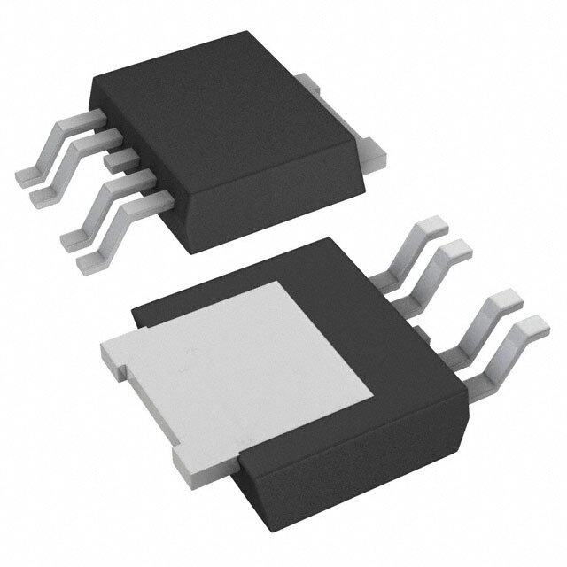
ICGOO电子元器件商城为您提供FDMC7208S由Fairchild Semiconductor设计生产,在icgoo商城现货销售,并且可以通过原厂、代理商等渠道进行代购。 FDMC7208S价格参考¥5.78-¥6.88。Fairchild SemiconductorFDMC7208S封装/规格:晶体管 - FET,MOSFET - 阵列, 2 个 N 沟道(双) Mosfet 阵列 30V 12A,16A 800mW 表面贴装 8-Power33(3x3)。您可以下载FDMC7208S参考资料、Datasheet数据手册功能说明书,资料中有FDMC7208S 详细功能的应用电路图电压和使用方法及教程。
FDMC7208S 是由 ON Semiconductor(安森美半导体)生产的一款晶体管 - FET,MOSFET - 阵列产品。它是一种双通道 N 沟道增强型 MOSFET 阵列,广泛应用于需要高效开关和低功耗的场景。以下是其主要应用场景:

 1. 电源管理
   - 负载切换:用于便携式设备(如智能手机、平板电脑等)中的负载切换,实现对不同电路模块的供电控制。
   - DC-DC 转换器:在降压或升压转换器中作为开关元件,提供高效的电压调节功能。
   - 电池保护:在电池管理系统中,用于防止过充、过放或短路。

 2. 信号切换
   - 在多路复用器或多路选择器中,用于切换不同的信号路径,适用于通信设备和数据采集系统。
   - 在音频设备中,用于切换输入/输出信号,实现多功能音频处理。

 3. 电机驱动
   - 用于小型直流电机或步进电机的驱动控制,支持正向和反向旋转以及速度调节。
   - 在消费电子产品的风扇控制中,提供高效的开关和调速功能。

 4. 固态继电器(SSR)
   - 替代传统机械继电器,用于工业控制、家电和照明系统的开关控制,具有更长的使用寿命和更高的可靠性。

 5. USB 和接口保护
   - 在 USB 接口或其他数据接口中,用于过流保护和热插拔保护,确保设备安全。

 6. 汽车电子
   - 应用于车载信息娱乐系统、车身控制模块(BCM)和传感器接口中,提供稳定的电源管理和信号切换功能。

 特性优势:
- 低导通电阻(Rds(on)):减少功率损耗,提高效率。
- 小型封装:节省 PCB 空间,适合紧凑型设计。
- 高开关速度:适用于高频应用,降低开关损耗。
- 出色的热性能:能够在高温环境下稳定工作。

综上所述,FDMC7208S 的应用场景涵盖了消费电子、通信设备、工业控制、汽车电子等多个领域,是一款高性能、多功能的 MOSFET 阵列器件。
| 参数 | 数值 |
| 产品目录 | |
| ChannelMode | Enhancement |
| 描述 | MOSFET 2N-CH 30V 12A/16A PWR33MOSFET 30V Dual N-Channel PowerTrench MOSFET |
| 产品分类 | FET - 阵列分离式半导体 |
| FET功能 | 逻辑电平门 |
| FET类型 | 2 个 N 沟道(双) |
| Id-ContinuousDrainCurrent | 12 A |
| Id-连续漏极电流 | 12 A, 16 A |
| 品牌 | Fairchild Semiconductor |
| 产品手册 | |
| 产品图片 |
|
| rohs | 符合RoHS无铅 / 符合限制有害物质指令(RoHS)规范要求 |
| 产品系列 | 晶体管,MOSFET,Fairchild Semiconductor FDMC7208SPowerTrench® |
| 数据手册 | |
| 产品型号 | FDMC7208S |
| Pd-PowerDissipation | 1.9 W |
| Pd-功率耗散 | 1.9 W |
| RdsOn-漏源导通电阻 | 9 mOhms, 6.4 mOhms |
| Vds-Drain-SourceBreakdownVoltage | 30 V |
| Vds-漏源极击穿电压 | 30 V |
| 不同Id时的Vgs(th)(最大值) | 3V @ 250µA |
| 不同Vds时的输入电容(Ciss) | 1130pF @ 15V |
| 不同Vgs时的栅极电荷(Qg) | 18nC @ 10V |
| 不同 Id、Vgs时的 RdsOn(最大值) | 9 毫欧 @ 12A,10V |
| 产品种类 | MOSFET |
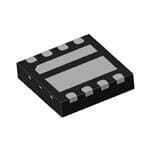
| 供应商器件封装 | Power33 |
| 其它名称 | FDMC7208SDKR |
| 功率-最大值 | 800mW |
| 包装 | Digi-Reel® |
| 单位重量 | 196 mg |
| 商标 | Fairchild Semiconductor |
| 安装类型 | 表面贴装 |
| 安装风格 | SMD/SMT |
| 封装 | Reel |
| 封装/外壳 | 8-PowerWDFN |
| 封装/箱体 | Power 33-8 |
| 工厂包装数量 | 3000 |
| 晶体管极性 | N-Channel |
| 最大工作温度 | + 150 C |
| 最小工作温度 | - 55 C |
| 标准包装 | 1 |
| 漏源极电压(Vdss) | 30V |
| 电流-连续漏极(Id)(25°C时) | 12A,16A |
| 系列 | FDMC7208 |
| 通道模式 | Enhancement |
| 配置 | Dual |


- 商务部:美国ITC正式对集成电路等产品启动337调查
- 曝三星4nm工艺存在良率问题 高通将骁龙8 Gen1或转产台积电
- 太阳诱电将投资9.5亿元在常州建新厂生产MLCC 预计2023年完工
- 英特尔发布欧洲新工厂建设计划 深化IDM 2.0 战略
- 台积电先进制程称霸业界 有大客户加持明年业绩稳了
- 达到5530亿美元!SIA预计今年全球半导体销售额将创下新高
- 英特尔拟将自动驾驶子公司Mobileye上市 估值或超500亿美元
- 三星加码芯片和SET,合并消费电子和移动部门,撤换高东真等 CEO
- 三星电子宣布重大人事变动 还合并消费电子和移动部门
- 海关总署:前11个月进口集成电路产品价值2.52万亿元 增长14.8%

PDF Datasheet 数据手册内容提取
Is Now Part of To learn more about ON Semiconductor, please visit our website at www.onsemi.com Please note: As part of the Fairchild Semiconductor integration, some of the Fairchild orderable part numbers will need to change in order to meet ON Semiconductor’s system requirements. Since the ON Semiconductor product management systems do not have the ability to manage part nomenclature that utilizes an underscore (_), the underscore (_) in the Fairchild part numbers will be changed to a dash (-). This document may contain device numbers with an underscore (_). Please check the ON Semiconductor website to verify the updated device numbers. The most current and up-to-date ordering information can be found at www.onsemi.com. Please email any questions regarding the system integration to Fairchild_questions@onsemi.com. ON Semiconductor and the ON Semiconductor logo are trademarks of Semiconductor Components Industries, LLC dba ON Semiconductor or its subsidiaries in the United States and/or other countries. ON Semiconductor owns the rights to a number of patents, trademarks, copyrights, trade secrets, and other intellectual property. A listing of ON Semiconductor’s product/patent coverage may be accessed at www.onsemi.com/site/pdf/Patent-Marking.pdf. ON Semiconductor reserves the right to make changes without further notice to any products herein. ON Semiconductor makes no warranty, representation or guarantee regarding the suitability of its products for any particular purpose, nor does ON Semiconductor assume any liability arising out of the application or use of any product or circuit, and specifically disclaims any and all liability, including without limitation special, consequential or incidental damages. Buyer is responsible for its products and applications using ON Semiconductor products, including compliance with all laws, regulations and safety requirements or standards, regardless of any support or applications information provided by ON Semiconductor. “Typical” parameters which may be provided in ON Semiconductor data sheets and/or specifications can and do vary in different applications and actual performance may vary over time. All operating parameters, including “Typicals” must be validated for each customer application by customer’s technical experts. ON Semiconductor does not convey any license under its patent rights nor the rights of others. ON Semiconductor products are not designed, intended, or authorized for use as a critical component in life support systems or any FDA Class 3 medical devices or medical devices with a same or similar classification in a foreign jurisdiction or any devices intended for implantation in the human body. Should Buyer purchase or use ON Semiconductor products for any such unintended or unauthorized application, Buyer shall indemnify and hold ON Semiconductor and its officers, employees, subsidiaries, affiliates, and distributors harmless against all claims, costs, damages, and expenses, and reasonable attorney fees arising out of, directly or indirectly, any claim of personal injury or death associated with such unintended or unauthorized use, even if such claim alleges that ON Semiconductor was negligent regarding the design or manufacture of the part. ON Semiconductor is an Equal Opportunity/Affirmative Action Employer. This literature is subject to all applicable copyright laws and is not for resale in any manner.
F D M C 7 July 2013 2 0 FDMC7208S 8 S ® D Dual N-Channel PowerTrench MOSFET u a Q1: 30 V, 12 A, 9.0 mΩ Q2: 30 V, 16 A, 6.4 mΩ l N Features General Description - C Q1: N-Channel This device includes two 30V N-Channel MOSFETs in a dual h a (cid:132) Max r = 9.0 mΩ at V = 10 V, I = 12 A Power 33 (3 mm X 3 mm MLP) package. The package is en- n DS(on) GS D hanced for exceptional thermal performance. n (cid:132) Max r = 11.0 mΩ at V = 4.5 V, I = 11 A e DS(on) GS D Applications l Q2: N-Channel P o (cid:132) Max r = 6.4 mΩ at V = 10 V, I = 16 A (cid:132) Computing w DS(on) GS D (cid:132) Communications e (cid:132) Max rDS(on) = 7.5 mΩ at VGS = 4.5 V, ID = 13.5 A rT (cid:132) Termination is Lead-free and RoHS Compliant (cid:132) General Purpose Point of Load re (cid:132) Notebook System n c h ® M Pin 1 O G1 S1 S1 S1 S F E D1 T D2 G2 S2 S2 S2 Power 33 MOSFET Maximum Ratings TA = 25 °C unless otherwise noted Symbol Parameter Q1 Q2 Units V Drain to Source Voltage 30 30 V DS V Gate to Source Voltage (Note 4) ±20 ±12 V GS Drain Current -Continuous (Package limited) T = 25 °C 22 26 C I -Continuous T = 25 °C 121a 161b A D A -Pulsed 60 80 E Single Pulse Avalanche Energy (Note 3) 21 21 mJ AS Power Dissipation for Single Operation T = 25 °C 1.91a 1.91b P A W D Power Dissipation for Single Operation T = 25 °C 0.81c 0.81d A T , T Operating and Storage Junction Temperature Range -55 to +150 °C J STG Thermal Characteristics R Thermal Resistance, Junction to Ambient 651a 651b θJA °C/W R Thermal Resistance, Junction to Ambient 1551c 1551d θJA Package Marking and Ordering Information Device Marking Device Package Reel Size Tape Width Quantity FDMC7208S FDMC7208S Power 33 13 ” 12 mm 3000 units ©2012 Fairchild Semiconductor Corporation 1 www.fairchildsemi.com FDMC7208S Rev.C3
F D Electrical Characteristics T = 25 °C unless otherwise noted M J C Symbol Parameter Test Conditions Type Min Typ Max Units 7 2 Off Characteristics 0 8 S I = 250 μA, V = 0 V Q1 30 BVDSS Drain to Source Breakdown Voltage ID = 1 mA, V G =S 0 V Q2 30 V D D GS u Δ BΔVTDJSS BCroeeaffkicdioewntn Voltage Temperature IIDD == 1205 0m μAA, ,r reefeferreenncceedd t oto 2 255 ° °CC QQ12 2271 mV/°C al N Q1 1 - I Zero Gate Voltage Drain Current V = 24 V, V = 0 V μA C DSS DS GS Q2 500 h Gate to Source Leakage Current, V = 20 V, V = 0 V Q1 100 a I GS DS nA n GSS Forward VGS = 12 V, VDS= 0 V Q2 100 n e On Characteristics l P I = 250 μA, V = 0 V Q1 1.2 1.7 3.0 o V Gate to Source Threshold Voltage D GS V w GS(th) I = 1 mA, V = 0 V Q2 1.2 1.6 3.0 D GS e ΔV Gate to Source Threshold Voltage I = 250 μA, referenced to 25 °C Q1 -5 r GS(th) D mV/°C T ΔTJ Temperature Coefficient ID = 10 mA, referenced to 25 °C Q2 -3 re V = 10 V, I = 12 A 6.7 9.0 n GS D V = 4.5 V, I = 11 A Q1 8.8 11.0 c GS D h rDS(on) Drain to Source On Resistance VVGS == 1100 VV,, IID == 1126 AA, T J = 125 °C 49..72 162.4.4 mΩ M® GS D V = 4.5 V, I = 13.5 A Q2 5.3 7.5 O GS D V = 10 V, I = 16 A , T = 125 °C 6.4 6.8 S GS D J F g Forward Transconductance VDS = 5 V, ID = 12 A Q1 53 S E FS VDS = 5 V, ID = 16 A Q2 80 T Dynamic Characteristics C Input Capacitance Q1: Q1 848 1130 pF iss V = 15 V, V = 0 V, f = 1 MHZ Q2 1685 2245 DS GS Q1 270 360 C Output Capacitance pF oss Q2: Q2 432 575 VDS = 15 V, VGS = 0 V, f = 1 MHZ Q1 36 55 C Reverse Transfer Capacitance pF rss Q2 42 65 Q1 0.1 1.1 2.5 R Gate Resistance Ω g Q2 0.1 1.0 2.5 Switching Characteristics Q1 6 12 t Turn-On Delay Time ns d(on) Q2 7 14 Q1: Q1 2 10 tr Rise Time VDD = 15 V, ID = 12 A, RGEN = 6 Ω Q2 3 10 ns Q1 16 29 t Turn-Off Delay Time Q2: ns d(off) Q2 23 36 V = 15 V, I = 16 A, R = 6 Ω DD D GEN Q1 2 10 t Fall Time ns f Q2 2 10 Q1 13 18 Qg Total Gate Charge VGS = 0 V to 10 V Q1 Q2 26 36 nC V = 15 V, DD Q1 6.7 9.4 Qg Total Gate Charge VGS = 0 V to 5 V ID = 12 A Q2 14 20 nC Q1 2.3 Qgs Gate to Source Gate Charge Q2 Q2 3.9 nC V = 15 V, DD Qgd Gate to Drain “Miller” Charge ID = 16 A QQ12 12..87 nC ©2012 Fairchild Semiconductor Corporation 2 www.fairchildsemi.com FDMC7208S Rev.C3
F D Electrical Characteristics T = 25 °C unless otherwise noted M J C Symbol Parameter Test Conditions Type Min Typ Max Units 7 2 Drain-Source Diode Characteristics 0 8 S V = 0 V, I = 2 A (Note 2) Q1 0.72 1.2 GS S V = 0 V, I = 12 A (Note 2) Q1 0.82 1.2 D VSD Source to Drain Diode Forward Voltage VGS = 0 V, IS = 2 A (Note 2) Q2 0.70 1.2 V u GS S a V = 0 V, I = 16 A (Note 2) Q2 0.82 1.2 l GS S N trr Reverse Recovery Time QI 1= 12 A, di/dt = 100 A/μs QQ12 2211 3343 ns -C F h Q2 Q1 6 12 a Qrr Reverse Recovery Charge IF = 16 A, di/dt = 300 A/μs Q2 16 28 nC nn Notes: e 1th.eR θuJsAe irs's d beotearrmd idneesdi gwni.th the device mounted on a 1 in2 pad 2 oz copper pad on a 1.5 x 1.5 in. board of FR-4 material. RθJC is guaranteed by design while RθCA is determined by l P o w b. 65 °C/W when mounted on e a . 6a5 1 ° iCn2/W pa wdh oefn 2m oozu nctoepdp oenr a 1 in2 pad of 2 oz copper rT r e n c h ® M O S F GDFDSSFSS GDFDSSFSS E T c. 155 °C/W when mounted on a d. 155 °C/W when mounted on a minimum pad of 2 oz copper minimum pad of 2 oz copper GDFDSSFSS GDFDSSFSS 2. Pulse Test: Pulse Width < 300 μs, Duty cycle < 2.0%. 3. Q1: EAS of 21 mJ is based on starting TJ = 25 oC, L = 0.3 mH, IAS = 12 A, VDD = 27 V, VGS = 10 V. 100% tested at L = 3 mH, IAS = 5.2 A. Q1: EAS of 21 mJ is based on starting TJ = 25 oC, L = 0.3 mH, IAS = 12 A, VDD = 27 V, VGS = 10 V. 100% tested at L = 3 mH, IAS = 5.4 A. 4. As an N-ch device, the negative Vgs rating is for low duty cycle pulse occurrence only. No continuous rating is implied ©2012 Fairchild Semiconductor Corporation 3 www.fairchildsemi.com FDMC7208S Rev.C3
F D Typical Characteristics (Q1 N-Channel) T = 25°C unless otherwise noted M J C 7 2 60 5 0 RENT (A) 4500 VGVSG S= V = 4G . 1S50 =V V 4V VGS = 3.5 V ZEDN-RESISTANCE 34 VGS = 3 V VGS = 3.5 PDVUULTSYE C DYUCRLEA T=I O0.N5 %= 8M0A μXs 8S Dual N UR 30 ALIE O -C DRAIN C 20 VGS = 3 V NORMO SOURC 2 VGS = 4 V hann I, D 10 PDUULTSYE C DYUCRLEA T=I O0.N5 %= 8M0A μXs RAIN T 1 VGS = 4.5 V VGS = 10 V el P 0 D 0 o 0 1 2 3 4 5 0 10 20 30 40 50 60 w VDS, DRAIN TO SO URCE VOLTAGE (V) ID, DRAIN CURR ENT (A) er T r Figure 1. On Region Characteristics Figure 2. Normalized On-Resistance e n vs Drain Current and Gate Voltage c h ® M 1.6 40 O STANCE 1.4 IVDG =S 1=2 1 A0 V ()E mΩ 30 ID = 12 A PDUULTSYE C DYUCRLEA T=I O0.N5 %= 8M0A μXs SFE NORMALIZED O SOURCE ON-RESI 11..02 rDRAIN TO ,DS(on)RCE ON-RESISTANC 1200 TJ = 125 oC T T 0.8 U N O AI S TJ = 25 oC R D 0.6 0 -75 -50 -25 0 25 50 75 100 125 150 2 3 4 5 6 7 8 9 10 TJ, JUNCTION TEM PERATURE (oC) VGS, GATE TO SOURCE VOLTAGE (V) Figure 3. Normalized On Resistance Figure 4. On-Resistance vs Gate to vs Junction Temperature Source Voltage 60 100 PULSE DURATION = 80 μs A) VGS = 0 V 50 DUTY CYCLE = 0.5% MAX NT ( 10 E T (A) 40 VDS = 5 V URR TJ = 150 oC RREN 30 TJ = 150 oC AIN C 1 U R N C TJ = 25 oC E D 0.1 TJ = 25 oC AI 20 RS R E I, DD 10 TJ = -55 oC , REVS0.01 TJ = -55 oC I 0 0.001 1.0 1.5 2.0 2.5 3.0 3.5 4.0 0.0 0.2 0.4 0.6 0.8 1.0 1.2 VGS, GATE TO SOU RCE VOLTAGE (V) VSD, BODY DIODE FOR WARD VOLTAGE (V) Figure 5. Transfer Characteristics Figure 6. Source to Drain Diode Forward Voltage vs Source Current ©2012 Fairchild Semiconductor Corporation 4 www.fairchildsemi.com FDMC7208S Rev.C3
F D Typical Characteristics (Q1 N-Channel) T = 25°C unless otherwise noted M J C 7 2 10 2000 0 8 GE (V) 8 ID = 12 A 1000 Ciss S D E TO SOURCE VOLTA 46 VDD = 10 VVDDV =D D1 5= V20 V CAPACITANCE (pF) 100 CCrossss ual N-Chann AT 2 f = 1 MHz e , GS VGS = 0 V l P VG 0 10 o 0 5 10 15 0.1 1 10 30 w Qg, GATE CH ARGE (nC) VDS, DRAIN TO SOU RCE VOLTAGE (V) er T r Figure 7. Gate Charge Characteristics Figure 8. Capacitance vs Drain e n to Source Voltage c h ® M 40 100 O S A) F T ( A) 10 E EN T ( T RR 10 EN U R E C TJ = 25 oC CUR 1 THIS AREA IS 1 ms VALANCH TJ = 125 oC TJ = 100 oC , DRAIN D 0.1 STLJIIMN =GI TMLEAEDX P B RUYAL SrTDEESD(on) 11100 s0 m mss , AS I RθJA = 155 oC/W DERIVED FROM 10 s IA TA = 25 oC TEST DATA DC 1 0.01 0.01 0.1 1 10 100 0.01 0.1 1 10 100 tAV, TIME IN AVA LANCHE (ms) VDS, DRAIN to SOU RCE VOLTAGE (V) Figure 9. Unclamped Inductive Figure 10. Forward Bias Safe Switching Capability Operating Area 110000 SINGLE PULSE ER (W) RTAθJ =A 2=5 1 o5C5 oC/W W O P T 10 N E NSI A R T K A E P , K) 1 P P( 0.5 10-3 10-2 10-1 100 101 100 1000 t, PULSE WIDTH (s ec) Figure 11. Single Pulse Maximum Power Dissipation ©2012 Fairchild Semiconductor Corporation 5 www.fairchildsemi.com FDMC7208S Rev.C3
F D Typical Characteristics (Q1 N-Channel) T = 25°C unless otherwise noted M J C 7 2 2 0 DUTY CYCLE-DESCENDING ORDER 8 1 S D = 0.5 D AL 0.2 u M A 0.1 a MALIZED THER ZMPEDANCE,Jθ 0.1 000...000521 PDM t1t2 l N-Chan ORI SINGLE PULSE NOTES: n N R = 155 oC/W DUTY FACTOR: D = t1/t2 e 0.01 (NθoJAte 1b) PEAK TJ = PDM x ZθJC x RθJc + TC l P o 0.005 w 10-3 10-2 10-1 100 101 100 1000 e t, RECTANGULAR PULSE DURATION (sec) rT r Figure 12. Junction-to-Ambient Transient Thermal Response Curve e n c h ® M O S F E T ©2012 Fairchild Semiconductor Corporation 6 www.fairchildsemi.com FDMC7208S Rev.C3
F D Typical Characteristics (Q2 N-Channel) T = 25 °C unless otherwise noted M J C 7 2 80 5 0 8 A) 60 VGVSG =S =4 . 51 0V V STANCE 4 VGS = 3 V S Du N CURRENT ( 40 VGVSG S= =3 . 54 VV VGS = 3 V ORMALIZEDURCE ON-RESI 23 PDUULTSYE C DYUCRLEA T=I OV0.NG5S %= = 8M 30A. 5μX sV al N-Cha AI NO n DR 20 O S n I, D PDUULTSYE C DYUCRLEA T=I O0.N5 %= 8M0A μXs AIN T 1 VGS = 4 V VGS = 4.5 V VGS = 10 V el P R 0 D 0 o 0.0 0.5 1.0 1.5 2.0 2.5 3.0 0 20 40 60 80 w VDS, DRAIN TO SO URCE VOLTAGE (V) ID, DRAIN CURR ENT (A) er T r Figure 14. On- Region Characteristics Figure 15. Normalized on-Resistance vs Drain e n Current and Gate Voltage c h ® M 1.5 30 O ANCE 1.4 IVDG =S 1=6 1 A0 V )mΩ 24 PDUULTSYE C DYUCRLEA T=I O0.N5 %= 8M0A μXs SF NORMALIZED TO SOURCE ON-RESIST 01111.....90123 rDRAIN TO ,DS(on)(URCE ON-RESISTANCE 11286 TIDJ == 11265 A oC ET RAIN 0.8 SO TJ = 25 oC D 0.7 0 -75 -50 -25 0 25 50 75 100 125 150 2 4 6 8 10 TJ, JUNCTION TEM PERATURE (oC) VGS, GATE TO SOURCE VOLTAGE (V) Figure 16. Normalized On-Resistance Figure 17. On-Resistance vs Gate to vs Junction Temperature Source Voltage 80 100 PULSE DURATION = 80 μs A) VGS = 0 V DUTY CYCLE = 0.5% MAX T ( 64 N 10 E T (A) VDS = 5 V URR TJ = 125 oC CURREN 48 TJ = 125 oC DRAIN C 1 TJ = 25 oC N 32 E 0.1 RAI TJ = 25 oC ERS TJ = -55 oC D V I, D 16 TJ = -55 oC I, RES0.01 0 0.001 1 2 3 4 0.0 0.2 0.4 0.6 0.8 1.0 1.2 VGS, GATE TO SOU RCE VOLTAGE (V) VSD, BODY DIODE FOR WARD VOLTAGE (V) Figure 18. Transfer Characteristics Figure 19. Source to Drain Diode Forward Voltage vs Source Current ©2012 Fairchild Semiconductor Corporation 7 www.fairchildsemi.com FDMC7208S Rev.C3
F D M Typical Characteristics (Q2 N-Channel) T = 25°C unless otherwise noted C J 7 2 0 10 3000 8 S GE (V) 8 ID = 16 A 1000 Ciss Du TO SOURCE VOLTA 46 VDD = 10 VVDD = 15V VDD = 20 V APACITANCE (pF) 100 Coss al N-Chann E C e GAT 2 f = 1 MHz Crss l P V, GS 0 10 VGS = 0 V ow 0 6 12 18 24 30 0.1 1 10 30 e Qg, GATE CH ARGE (nC) VDS, DRAIN TO SOU RCE VOLTAGE (V) rT r e Figure 20. Gate Charge Characteristics Figure 21. Capacitance vs Drain n c to Source Voltage h ® M 40 100 O S F A) E T ( A) 10 T EN T ( CURR 10 TJ = 25 oC RREN 1 ms E CU 1 THIS AREA IS ANCH TJ = 125 oC TJ = 100 oC RAIN SLIIMNGITLEED P BUYL SrDES(on) 1100 0m mss L D VA , D 0.1 TJ = MAX RATED 1 s I, AAS I RTAθJ =A 2=5 1 o5C5 oC/W DTEESRTIV DEADT FAROM D10C s 1 0.01 0.001 0.01 0.1 1 10 100 0.01 0.1 1 10 100 tAV, TIME IN AVA LANCHE (ms) VDS, DRAIN to SOU RCE VOLTAGE (V) Figure 22. Unclamped Inductive Figure 23. Forward Bias Safe Switching Capability Operating Area 110000 SINGLE PULSE ER (W) RTAθJ =A 2=5 1 o5C5 oC/W W O P T 10 N E NSI A R T K A E P , K) 1 P P( 0.5 10-3 10-2 10-1 100 101 100 1000 t, PULSE WIDTH (s ec) Figure 24. Single Pulse Maximum Power Dissipation ©2012 Fairchild Semiconductor Corporation 8 www.fairchildsemi.com FDMC7208S Rev.C3
F D Typical Characteristics (Q2 N-Channel) M T = 25 °C unless otherwise noted J C 7 2 2 0 DUTY CYCLE-DESCENDING ORDER 8 1 S D = 0.5 D AL 0.2 u M A 0.1 a D THER NCE,ZJθ 0.1 000...000521 PDM l N-C MALIZEMPEDA t1t2 han ORI SINGLE PULSE NOTES: n N R = 155 oC/W DUTY FACTOR: D = t1/t2 e 0.01 (NθoJAte 1b) PEAK TJ = PDM x ZθJC x RθJC + TC l P o 0.005 w 10-3 10-2 10-1 100 101 100 1000 e r t, RECTANGULAR PULSE DURATION (sec) T r e Figure 26. Junction-to-Ambient Transient Thermal Response Curve n c h ® M O S F E T ©2012 Fairchild Semiconductor Corporation 9 www.fairchildsemi.com FDMC7208S Rev.C3
F D Typical Characteristics M (continued) C 7 2 0 SyncFETTM Schottky body diode 8 S Characteristics D u Fairchild’s SyncFETTM process embeds a Schottky diode in Schottky barrier diodes exhibit significant leakage at high tem- a parallel with PowerTrench MOSFET. This diode exhibits similar perature and high reverse voltage. This will increase the power l N characteristics to a discrete external Schottky diode in parallel in the device. - C with a MOSFET. Figure 27 shows the reverses recovery h characteristic of the FDMC7208S. a n n 20 10-2 e T (A) TJ = 125 oC l P 15 EN10-3 o R w R U e ENT (A) 10 KAGE C10-4 TJ = 100 oC rTre CURR 5 E LEA10-5 nch 0 VERS10-6 TJ = 25 oC M® E R O -5 I, DSS10-70 5 10 15 20 25 30 SF 0 40 80 120 160 200 E TIME (ns) VDS, REVERSE VOLTAGE (V) T Figure 27. FDMC7208S SyncFETTM body Figure 28. SyncFETTM body diode reverses diode reverse recovery characteristic leakage versus drain-source voltage ©2012 Fairchild Semiconductor Corporation 10 www.fairchildsemi.com FDMC7208S Rev.C3
F D Dimensional Outline and Pad Layout M C 7 2 0 8 S D u a l N - C h a n n e l P o w e r T r e n c h ® M O S F E T ©2012 Fairchild Semiconductor Corporation 11 www.fairchildsemi.com FDMC7208S Rev.C3
F D M C 7 2 0 8 S TRADEMARKS D The following includes registered and unregistered trademarks and service marks, owned by Fairchild Semiconductor and/or its global subsidiaries, and is not u intended to be an exhaustive list of all such trademarks. a l 2Cool™ FPS™ Sync-Lock™ N AAcXc-CuPAoPw®e*r™ FF-RPFFEST™® Powtm®erTrench® ®* -C BitSiC™ Global Power ResourceSM PowerXS™ h Build it Now™ Green Bridge™ Programmable Active Droop™ TinyBoost™ a CorePLUS™ Green FPS™ QFET® TinyBuck™ n TinyCalc™ n CorePOWER™ Green FPS™ e-Series™ QS™ TinyLogic® e CROSSVOLT™ Gmax™ Quiet Series™ TINYOPTO™ l CTL™ GTO™ RapidConfigure™ P TinyPower™ Current Transfer Logic™ IntelliMAX™ ™ o DEUXPEED® ISOPLANAR™ TinyPWM™ w TinyWire™ DEcuoaSl CPAooRl™K® Manadr kBinegtt eSrm™all Speakers Sound Louder SSiagvninaglW oiuser ™world, 1mW/W/kW at a time™ TranSiC® er TriFault Detect™ T EfficentMax™ MegaBuck™ SmartMax™ TRUECURRENT®* r ESBC™ MICROCOUPLER™ SMART START™ e MicroFET™ Solutions for Your Success™ μSerDes™ n ® MicroPak™ SPM® c h FFFAaaiiCrrccThh iiQllddu® Sieet mSiecroiensd™uctor® MMMiiocllterioorDPnMraivkae2x™™™ SSSuuTppEeeArrLSFTEOHTT™®™-3 UUlHtrCa ®FRFET™ M® FACT® mWSaver™ SuperSOT™-6 UniFET™ O FAST® OptoHiT™ SuperSOT™-8 VCX™ S FastvCore™ OPTOLOGIC® SupreMOS® VisualMax™ F FETBench™ OPTOPLANAR® SyncFET™ VoltagePlus™ E XS™ T *Trademarks of System General Corporation, used under license by Fairchild Semiconductor. DISCLAIMER FAIRCHILD SEMICONDUCTOR RESERVES THE RIGHT TO MAKE CHANGES WITHOUT FURTHER NOTICE TO ANY PRODUCTS HEREIN TO IMPROVE RELIABILITY, FUNCTION, OR DESIGN. FAIRCHILD DOES NOT ASSUME ANY LIABILITY ARISING OUT OF THE APPLICATION OR USE OF ANY PRODUCT OR CIRCUIT DESCRIBED HEREIN; NEITHER DOES IT CONVEY ANY LICENSE UNDER ITS PATENT RIGHTS, NOR THE RIGHTS OF OTHERS. THESE SPECIFICATIONS DO NOT EXPAND THE TERMS OF FAIRCHILD’S WORLDWIDE TERMS AND CONDITIONS, SPECIFICALLY THE WARRANTY THEREIN, WHICH COVERS THESE PRODUCTS. LIFE SUPPORT POLICY FAIRCHILD’S PRODUCTS ARE NOT AUTHORIZED FOR USE AS CRITICAL COMPONENTS IN LIFE SUPPORT DEVICES OR SYSTEMS WITHOUT THE EXPRESS WRITTEN APPROVAL OF FAIRCHILD SEMICONDUCTOR CORPORATION. As used here in: 1. Life support devices or systems are devices or systems which, (a) are 2. A critical component in any component of a life support, device, or intended for surgical implant into the body or (b) support or sustain life, system whose failure to perform can be reasonably expected to cause and (c) whose failure to perform when properly used in accordance with the failure of the life support device or system, or to affect its safety or instructions for use provided in the labeling, can be reasonably effectiveness. expected to result in a significant injury of the user. ANTI-COUNTERFEITING POLICY Fairchild Semiconductor Corporation’s Anti-Counterfeiting Policy. Fairchild’s Anti-Counterfeiting Policy is also stated on our external website, www.Fairchildsemi.com, under Sales Support. Counterfeiting of semiconductor parts is a growing problem in the industry. All manufactures of semiconductor products are experiencing counterfeiting of their parts. Customers who inadvertently purchase counterfeit parts experience many problems such as loss of brand reputation, substandard performance, failed application, and increased cost of production and manufacturing delays. Fairchild is taking strong measures to protect ourselves and our customers from the proliferation of counterfeit parts. Fairchild strongly encourages customers to purchase Fairchild parts either directly from Fairchild or from Authorized Fairchild Distributors who are listed by country on our web page cited above. Products customers buy either from Fairchild directly or from Authorized Fairchild Distributors are genuine parts, have full traceability, meet Fairchild’s quality standards for handing and storage and provide access to Fairchild’s full range of up-to-date technical and product information. Fairchild and our Authorized Distributors will stand behind all warranties and will appropriately address and warranty issues that may arise. Fairchild will not provide any warranty coverage or other assistance for parts bought from Unauthorized Sources. Fairchild is committed to combat this global problem and encourage our customers to do their part in stopping this practice by buying direct or from authorized distributors. PRODUCT STATUS DEFINITIONS Definition of Terms Datasheet Identification Product Status Definition Datasheet contains the design specifications for product development. Specifications Advance Information Formative / In Design may change in any manner without notice. Datasheet contains preliminary data; supplementary data will be published at a later Preliminary First Production date. Fairchild Semiconductor reserves the right to make changes at any time without notice to improve design. Datasheet contains final specifications. Fairchild Semiconductor reserves the right to No Identification Needed Full Production make changes at any time without notice to improve the design. Datasheet contains specifications on a product that is discontinued by Fairchild Obsolete Not In Production Semiconductor. The datasheet is for reference information only. Rev. I64 ©2012 Fairchild Semiconductor Corporation 12 www.fairchildsemi.com FDMC7208S Rev.C3
ON Semiconductor and are trademarks of Semiconductor Components Industries, LLC dba ON Semiconductor or its subsidiaries in the United States and/or other countries. ON Semiconductor owns the rights to a number of patents, trademarks, copyrights, trade secrets, and other intellectual property. A listing of ON Semiconductor’s product/patent coverage may be accessed at www.onsemi.com/site/pdf/Patent−Marking.pdf. ON Semiconductor reserves the right to make changes without further notice to any products herein. ON Semiconductor makes no warranty, representation or guarantee regarding the suitability of its products for any particular purpose, nor does ON Semiconductor assume any liability arising out of the application or use of any product or circuit, and specifically disclaims any and all liability, including without limitation special, consequential or incidental damages. Buyer is responsible for its products and applications using ON Semiconductor products, including compliance with all laws, regulations and safety requirements or standards, regardless of any support or applications information provided by ON Semiconductor. “Typical” parameters which may be provided in ON Semiconductor data sheets and/or specifications can and do vary in different applications and actual performance may vary over time. All operating parameters, including “Typicals” must be validated for each customer application by customer’s technical experts. ON Semiconductor does not convey any license under its patent rights nor the rights of others. ON Semiconductor products are not designed, intended, or authorized for use as a critical component in life support systems or any FDA Class 3 medical devices or medical devices with a same or similar classification in a foreign jurisdiction or any devices intended for implantation in the human body. Should Buyer purchase or use ON Semiconductor products for any such unintended or unauthorized application, Buyer shall indemnify and hold ON Semiconductor and its officers, employees, subsidiaries, affiliates, and distributors harmless against all claims, costs, damages, and expenses, and reasonable attorney fees arising out of, directly or indirectly, any claim of personal injury or death associated with such unintended or unauthorized use, even if such claim alleges that ON Semiconductor was negligent regarding the design or manufacture of the part. ON Semiconductor is an Equal Opportunity/Affirmative Action Employer. This literature is subject to all applicable copyright laws and is not for resale in any manner. PUBLICATION ORDERING INFORMATION LITERATURE FULFILLMENT: N. American Technical Support: 800−282−9855 Toll Free ON Semiconductor Website: www.onsemi.com Literature Distribution Center for ON Semiconductor USA/Canada 19521 E. 32nd Pkwy, Aurora, Colorado 80011 USA Europe, Middle East and Africa Technical Support: Order Literature: http://www.onsemi.com/orderlit Phone: 303−675−2175 or 800−344−3860 Toll Free USA/Canada Phone: 421 33 790 2910 Fax: 303−675−2176 or 800−344−3867 Toll Free USA/Canada Japan Customer Focus Center For additional information, please contact your local Email: orderlit@onsemi.com Phone: 81−3−5817−1050 Sales Representative © Semiconductor Components Industries, LLC www.onsemi.com www.onsemi.com 1
Mouser Electronics Authorized Distributor Click to View Pricing, Inventory, Delivery & Lifecycle Information: O N Semiconductor: FDMC7208S