ICGOO在线商城 > 分立半导体产品 > 晶体管 - FET,MOSFET - 阵列 > NTHD4508NT1G
 Datasheet下载
- 型号: NTHD4508NT1G
- 制造商: ON Semiconductor
- 库位|库存: xxxx|xxxx
- 要求:
| 数量阶梯 | 香港交货 | 国内含税 |
| +xxxx | $xxxx | ¥xxxx |
查看当月历史价格
查看今年历史价格
NTHD4508NT1G产品简介:
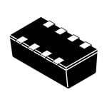
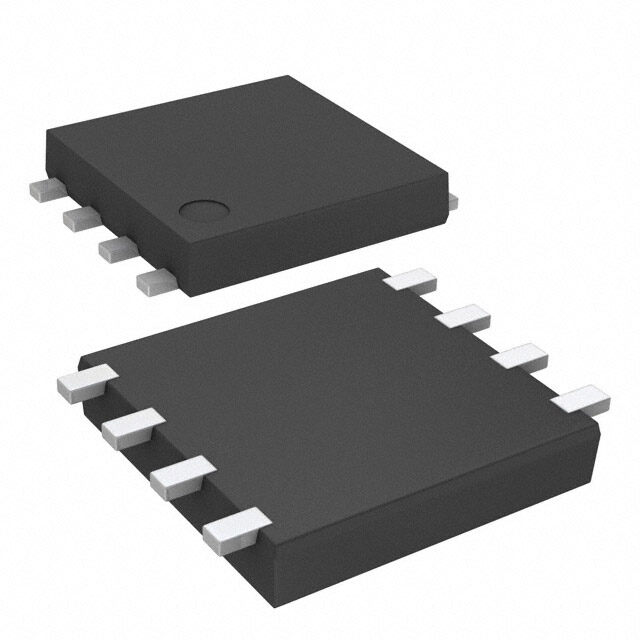
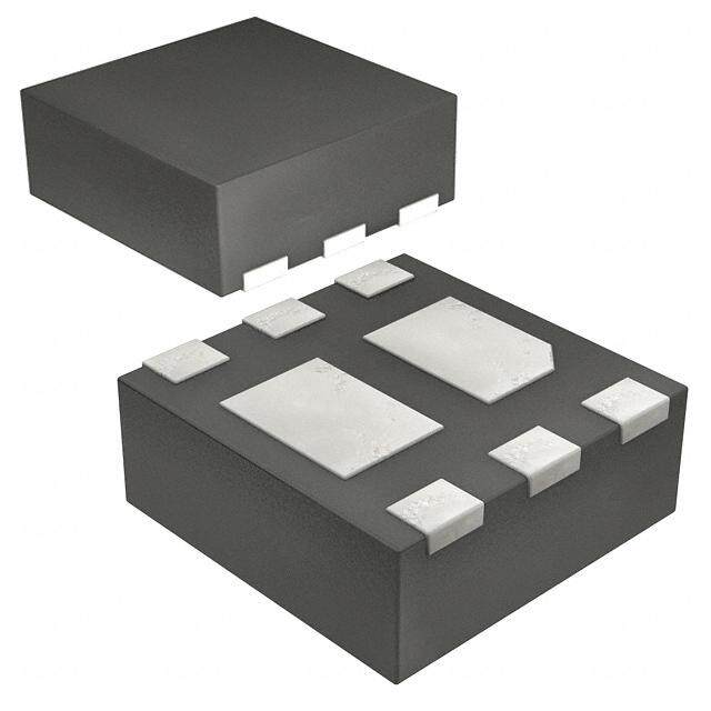
ICGOO电子元器件商城为您提供NTHD4508NT1G由ON Semiconductor设计生产,在icgoo商城现货销售,并且可以通过原厂、代理商等渠道进行代购。 NTHD4508NT1G价格参考。ON SemiconductorNTHD4508NT1G封装/规格:晶体管 - FET,MOSFET - 阵列, 2 个 N 沟道(双) Mosfet 阵列 20V 3A 1.13W 表面贴装 ChipFET™。您可以下载NTHD4508NT1G参考资料、Datasheet数据手册功能说明书,资料中有NTHD4508NT1G 详细功能的应用电路图电压和使用方法及教程。
NTHD4508NT1G 是由 ON Semiconductor(安森美半导体)生产的一款双通道 N 沟道增强型 MOSFET 阵列,属于晶体管 - FET、MOSFET - 阵列类别。该型号具有低导通电阻和快速开关特性,适用于多种电子电路设计场景。以下是其主要应用场景:

 1. 电源管理
   - 负载切换:用于控制负载的开启和关闭,例如在电池供电设备中切换不同的工作模式。
   - DC-DC 转换器:作为开关元件,用于降压或升压转换器中,实现高效的电压调节。
   - 线性稳压器:通过动态调整 MOSFET 的导通状态来优化输出电压稳定性。

 2. 电机驱动
   - 小型直流电机控制:用于驱动玩具、家用电器中的小型直流电机,提供正转、反转及调速功能。
   - H 桥电路:与其他 MOSFET 配合,构建 H 桥以实现电机的双向控制。

 3. 信号切换与保护
   - 信号路径切换:在多路复用器或多路选择器中,用于切换不同的信号路径。
   - 过流保护:通过检测电流并限制过载情况,保护下游电路免受损害。
   - ESD 和浪涌保护:利用其快速响应能力,防止静电放电和瞬态电压对敏感电路的影响。

 4. 消费类电子产品
   - 音频设备:用于耳机放大器或扬声器驱动电路,提供高效率和低失真的性能。
   - 便携式设备:如智能手机、平板电脑等,用于充电管理和电池保护电路。

 5. 工业自动化
   - 传感器接口:为各种传感器提供电源或信号隔离。
   - 继电器替代:用作固态继电器,减少机械磨损并提高可靠性。

 6. 汽车电子
   - 车灯控制:用于 LED 灯条或尾灯的亮度调节。
   - 车载信息娱乐系统:实现音频放大和电源管理功能。

NTHD4508NT1G 的双通道设计使其能够同时控制两个独立的负载或信号路径,非常适合需要紧凑布局和高效性能的应用场合。此外,其低导通电阻特性有助于降低功耗,提高整体系统的能效比。
| 参数 | 数值 |
| 产品目录 | |
| ChannelMode | Enhancement |
| 描述 | MOSFET 2N-CH 20V 3A CHIPFETMOSFET 20V 4.1A Dual N-Channel |
| 产品分类 | FET - 阵列分离式半导体 |
| FET功能 | 逻辑电平门 |
| FET类型 | 2 个 N 沟道(双) |
| Id-ContinuousDrainCurrent | 4.1 A |
| Id-连续漏极电流 | 4.1 A |
| 品牌 | ON Semiconductor |
| 产品手册 | |
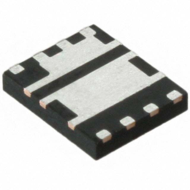
| 产品图片 |
|
| rohs | 符合RoHS无铅 / 符合限制有害物质指令(RoHS)规范要求 |
| 产品系列 | 晶体管,MOSFET,ON Semiconductor NTHD4508NT1G- |
| 数据手册 | |
| 产品型号 | NTHD4508NT1G |
| Pd-PowerDissipation | 1.13 W |
| Pd-功率耗散 | 1.13 W |
| RdsOn-Drain-SourceResistance | 80 mOhms |
| RdsOn-漏源导通电阻 | 80 mOhms |
| Vds-Drain-SourceBreakdownVoltage | 20 V |
| Vds-漏源极击穿电压 | 20 V |
| Vgs-Gate-SourceBreakdownVoltage | +/- 12 V |
| Vgs-栅源极击穿电压 | 12 V |
| 上升时间 | 15 ns |
| 下降时间 | 15 ns |
| 不同Id时的Vgs(th)(最大值) | 1.2V @ 250µA |
| 不同Vds时的输入电容(Ciss) | 180pF @ 10V |
| 不同Vgs时的栅极电荷(Qg) | 4nC @ 4.5V |
| 不同 Id、Vgs时的 RdsOn(最大值) | 75 毫欧 @ 3.1A,4.5V |
| 产品目录页面 | |
| 产品种类 | MOSFET |
| 供应商器件封装 | ChipFET™ |
| 其它名称 | NTHD4508NT1GOSTR |
| 典型关闭延迟时间 | 10 ns |
| 功率-最大值 | 1.13W |
| 功率耗散 | 1.13 W |
| 包装 | 带卷 (TR) |
| 商标 | ON Semiconductor |
| 安装类型 | 表面贴装 |
| 安装风格 | SMD/SMT |
| 导通电阻 | 80 mOhms |
| 封装 | Reel |
| 封装/外壳 | 8-SMD,扁平引线 |
| 封装/箱体 | 1206-8 ChipFET |
| 工厂包装数量 | 3000 |
| 晶体管极性 | N-Channel |
| 最大工作温度 | + 150 C |
| 最小工作温度 | - 55 C |
| 标准包装 | 3,000 |
| 正向跨导-最小值 | 6 S |
| 汲极/源极击穿电压 | 20 V |
| 漏极连续电流 | 4.1 A |
| 漏源极电压(Vdss) | 20V |
| 电流-连续漏极(Id)(25°C时) | 3A |
| 系列 | NTHD4508N |
| 通道模式 | Enhancement |
| 配置 | Dual Dual Drain |
| 闸/源击穿电压 | +/- 12 V |


- 商务部:美国ITC正式对集成电路等产品启动337调查
- 曝三星4nm工艺存在良率问题 高通将骁龙8 Gen1或转产台积电
- 太阳诱电将投资9.5亿元在常州建新厂生产MLCC 预计2023年完工
- 英特尔发布欧洲新工厂建设计划 深化IDM 2.0 战略
- 台积电先进制程称霸业界 有大客户加持明年业绩稳了
- 达到5530亿美元!SIA预计今年全球半导体销售额将创下新高
- 英特尔拟将自动驾驶子公司Mobileye上市 估值或超500亿美元
- 三星加码芯片和SET,合并消费电子和移动部门,撤换高东真等 CEO
- 三星电子宣布重大人事变动 还合并消费电子和移动部门
- 海关总署:前11个月进口集成电路产品价值2.52万亿元 增长14.8%


PDF Datasheet 数据手册内容提取
NTHD4508N MOSFET – Power, Dual, N-Channel, ChipFET 20 V, 4.1 A Features • http://onsemi.com Low R and Fast Switching Speed DS(on) • Leadless ChipFET Package has 40% Smaller Footprint than TSOP−6 • Excellent Thermal Capabilities Where Heat Transfer is Required V(BR)DSS RDS(on) TYP ID MAX • Pb−Free Package is Available 60 m(cid:2) @ 4.5 V 20 V 4.1 A Applications 80 m(cid:2) @ 2.5 V • DC−DC Buck/Boost Converters • Battery and Low Side Switching in Portable Equipment Such as MP3 D1, D2 Players, Cell Phones, DSCs and PDAs • Level Shifting MAXIMUM RATINGS (TJ = 25°C unless otherwise noted) G1, G2 Parameter Symbol Value Unit Drain−to−Source Voltage VDSS 20 V S1, S2 Gate−to−Source Voltage VGS ±12 V N−Channel MOSFET Continuous Drain Steady TJ = 25 °C ID 3.0 A Current State TJ = 85 °C 2.2 ChipFET CASE 1206A t (cid:2) 5 s TJ = 25 °C 4.1 STYLE 2 Power Dissipation Steady TJ = 25 °C PD 1.13 W State TJ = 85 °C 0.59 PIN MARKING t (cid:2) 5 s TJ = 25 °C 2.1 CONNECTIONS DIAGRAM Pulsed Drain Current tp = 10 μs IDM 12 A Operating Junction and Storage Temperature TTSJT,G −15550 to °C D1 8 1 S1 1 8 Lead Temperature for Soldering Purposes TL 260 °C D1 7 2 G1 2 C8 7 (1/8” from case for 10 s) D2 6 3 S2 3 M 6 THERMAL RESISTANCE RATINGS Parameter Symbol Max Unit D2 5 4 G2 4 5 Junction−to−Ambient – Steady State RθJA 110 °C/W (Note 1) C8= Specific Device Code M = Month Code Maximum ratings are those values beyond which device damage can occur. Maximum ratings applied to the device are individual stress limit values (not normal operating conditions) and are not valid simultaneously. If these limits are exceeded, device functional operation is not implied, damage may occur and ORDERING INFORMATION reliability may be affected. 1. Surface Mounted on FR4 Board using 1 in sq pad size (Cu area = 1.27 in sq Device Package Shipping† [1 oz] including traces). NTHD4508NT1 ChipFET 3000/Tape & Reel ChipFET NTHD4508NT1G 3000/Tape & Reel (Pb−Free) †For information on tape and reel specifications, including part orientation and tape sizes, please refer to our Tape and Reel Packaging Specification Brochure, BRD8011/D. © Semiconductor Components Industries, LLC, 2004 1 Publication Order Number: May, 2019 − Rev. 3 NTHD4508N/D
NTHD4508N ELECTRICAL CHARACTERISTICS (TJ = 25°C unless otherwise noted) Parameter Symbol Test Conditions Min Typ Max Units OFF CHARACTERISTICS Drain−to−Source Breakdown Voltage V(BR)DSS VGS = 0 V 20 V Zero Gate Voltage Drain Current IDSS VGS = 0 V, VDS = 16 V 1.0 (cid:3)A VGS = 0 V, VDS = 16 V, TJ = 125°C 10 Gate−to−Source Leakage Current IGSS VDS = 0 V, VGS = (cid:3)12 V (cid:3)100 nA ON CHARACTERISTICS (Note 2) Gate Threshold Voltage VGS(TH) VGS = VDS, ID = 250 (cid:3)A 0.6 1.2 V Drain−to−Source On−Resistance RDS(on) VGS = 4.5, ID = 3.1 A 60 75 m(cid:2) VGS = 2.5, ID = 2.3 A 80 115 Forward Transconductance gFS VDS = 10 V, ID = 3.1 A 6.0 S CHARGES AND CAPACITANCES Input Capacitance CISS 180 pF Output Capacitance COSS VGS = V0D VS, =f =1 01 .V0 MHz, 80 Reverse Transfer Capacitance CRSS 25 Total Gate Charge QG(TOT) 2.6 4.0 nC Threshold Gate Charge QG(TH) VGS = 4.5 V, VDS = 10 V, 0.5 Gate−to−Source Charge QGS ID = 3.1 A 0.6 Gate−to−Drain Charge QGD 0.7 SWITCHING CHARACTERISTICS (Note 3) Turn−On Delay Time td(ON) 5.0 10 ns Rise Time tr VGS = 4.5 V, VDS = 16 V, 15 30 Turn−Off Delay Time td(OFF) ID = 3.1 A, RG = 2.5 (cid:2) 10 20 Fall Time tf 3.0 6.0 DRAIN−SOURCE DIODE CHARACTERISTICS Forward Diode Voltage VSD VGS = 0 V, IS = 3.1 A 0.75 1.15 V Reverse Recovery Time tRR 12.5 ns Charge Time ta 9.0 VGS = 0 V, IS = 1.5 A, Discharge Time tb dIS/dt = 100 A/(cid:3)s 3.5 Reverse Recovery Charge QRR 6.0 nC 2. Pulse Test: Pulse Width (cid:2) 300 (cid:3)s, Duty Cycle (cid:2) 2%. 3. Switching characteristics are independent of operating junction temperatures. http://onsemi.com 2
NTHD4508N TYPICAL PERFORMANCE CURVES (TJ = 25°C unless otherwise noted) 8 8 VGS = 5 V to 3 V TJ = 25°C VDS ≥ 10 V S) VGS = 2.4 V S) P 2.2 V 2 V P M 6 M 6 A A T ( T ( N N E E RR 4 1.8 V RR 4 U U C C N N AI AI DR 2 1.6 V DR 2 TC = −55°C D, D, I 1.4 V I 25°C 100°C 0 0 0 1 2 3 4 5 6 7 8 9 10 0 0.5 1 1.5 2 2.5 3 VDS, DRAIN−TO−SOURCE VOLTAGE (VOLTS) VGS, GATE−TO−SOURCE VOLTAGE (VOLTS) Figure 1. On−Region Characteristics Figure 2. Transfer Characteristics (cid:2)) (cid:2)) E (0.15 E ( 0.1 NC ID = 3.1 A NC TJ = 25°C STA TJ = 25°C STA ESI ESI VGS = 2.5 V E R0.10 E R C C R R U U 0.07 O O N−TO−S0.05 N−TO−S VGS = 4.5 V AI AI R R D D R DS(on), 00 1 2 3 4 5 6 R DS(on), 0.04 1 3 5 7 VGS, GATE−TO−SOURCE VOLTAGE (VOLTS) ID, DRAIN CURRENT (AMPS) Figure 3. On−Resistance vs. Gate−to−Source Figure 4. On−Resistance vs. Drain Current and Voltage Gate Voltage 1.7 100 ID = 3.1 A VGS = 0 V ED) VGS = 4.5 V RCZE 1.5 DRAIN−TO−SOU S(on),SISTANCE (NORMALI 110...319 I, LEAKAGE (nA)DSS 10 TJ = 100°C DE RR 0.7 1 −50 −25 0 25 50 75 100 125 150 2 4 6 8 10 12 14 16 18 20 TJ, JUNCTION TEMPERATURE (°C) VDS, DRAIN−TO−SOURCE VOLTAGE (VOLTS) Figure 5. On−Resistance Variation with Figure 6. Drain−to−Source Leakage Current Temperature vs. Voltage http://onsemi.com 3
NTHD4508N TYPICAL PERFORMANCE CURVES (TJ = 25°C unless otherwise noted) 400 CISS VDS = 0 V VGS = 0 V TJ = 25°C OLTS)5 QG 10 OLTS) V V TANCE (pF) 320000 CRSS E VOLTAGE (43 7.5E VOLTAGE ( PACI URC2 QGS QGD 5.0URC A O O C S S C, 100 O− 2.5O− COSS −T1 −T E ID = 3.1 A N 0 GAT0 TJ = 25°C 0 DRAI 10 5 VGS0 VDS 5 10 15 20 V GS, 0 0.5 QG, TO1TAL GA1T.E5 CHARG2E (nC) 2.5 3 V DS, GATE−TO−SOURCE OR DRAIN−TO−SOURCE VOLTAGE (VOLTS) Figure 8. Gate−to−Source and Figure 7. Capacitance Variation Drain−to−Source Voltage vs. Total Charge 100 7 VIDD =D 2=. 31 6A V PS) 6 VTJG =S =2 50° CV VGS = 4.5 V AM T ( 5 s) EN ME (n 10 td(off) URR 4 t, TI td(ontr) CE C 3 R tf U 2 O S , S 1 I 1 0 1 10 100 0.3 0.45 0.6 0.75 0.9 1.05 1.2 RG, GATE RESISTANCE (OHMS) VSD, SOURCE−TO−DRAIN VOLTAGE (VOLTS) Figure 9. Resistive Switching Time Variation Figure 10. Diode Forward Voltage vs. Current vs. Gate Resistance http://onsemi.com 4
NTHD4508N SOLDERING FOOTPRINTS* 2.032 2.032 0.08 0.08 0.457 0.018 0.635 0.635 1.032 0.025 0.025 0.043 0.178 0.007 0.457 0.018 0.711 0.254 0.028 0.010 0.66 0.66 (cid:4) (cid:5) mm 0.026 0.026 SCALE 20:1 inches Figure 11. Basic Figure 12. Style 2 *For additional information on our Pb−Free strategy and soldering details, please download the ON Semiconductor Soldering and Mounting Techniques Reference Manual, SOLDERRM/D. BASIC PAD PATTERNS The basic pad layout with dimensions is shown in footprint. The drain copper area is 0.0019 sq. in. (or 1.22 sq. Figure 11. This is sufficient for low power dissipation mm). This will assist the power dissipation path away from MOSFET applications, but power semiconductor the device (through the copper lead−frame) and into the performance requires a greater copper pad area, particularly board and exterior chassis (if applicable) for the single for the drain leads. device. The addition of a further copper area and/or the The minimum recommended pad pattern shown in Figure addition of vias to other board layers will enhance the 12 improves the thermal area of the drain connections (pins performance still further. 5, 6, 7, 8) while remaining within the confines of the basic http://onsemi.com 5
NTHD4508N PACKAGE DIMENSIONS ChipFET CASE 1206A−03 ISSUE E NOTES: 1. DIMENSIONING AND TOLERANCING PER ANSI Y14.5M, 1982. 2. CONTROLLING DIMENSION: MILLIMETER. A M 3. MOLD GATE BURRS SHALL NOT EXCEED 0.13 MM PER SIDE. 4. LEADFRAME TO MOLDED BODY OFFSET IN K 8 7 6 5 HORIZONTAL AND VERTICAL SHALL NOT EXCEED 5 6 7 8 0.08 MM. 5. DIMENSIONS A AND B EXCLUSIVE OF MOLD GATE S B BURRS. 4 3 2 1 6. NO MOLD FLASH ALLOWED ON THE TOP AND 1 2 3 4 BOTTOM LEAD SURFACE. 7. 1206A-01 AND 1206A-02 OBSOLETE. NEW STANDARD IS 1206A-03. L D J MILLIMETERS INCHES G DIM MIN MAX MIN MAX STYLE 2: A 2.95 3.10 0.116 0.122 PIN 1.SOURCE 1 B 1.55 1.70 0.061 0.067 2.GATE 1 C 1.00 1.10 0.039 0.043 3.SOURCE 2 D 0.25 0.35 0.010 0.014 4.GATE 2 G 0.65 BSC 0.025 BSC C 56..DDRRAAIINN 22 KJ 00..1208 00..2402 00..000141 00..001078 7.DRAIN 1 L 0.55 BSC 0.022 BSC 0.05 (0.002) 8.DRAIN 1 M 5 ° NOM 5 ° NOM S 1.80 2.00 0.072 0.080 ChipFET is a trademark of Vishay Siliconix. ON Semiconductor and are registered trademarks of Semiconductor Components Industries, LLC (SCILLC). SCILLC reserves the right to make changes without further notice to any products herein. SCILLC makes no warranty, representation or guarantee regarding the suitability of its products for any particular purpose, nor does SCILLC assume any liability arising out of the application or use of any product or circuit, and specifically disclaims any and all liability, including without limitation special, consequential or incidental damages. “Typical” parameters which may be provided in SCILLC data sheets and/or specifications can and do vary in different applications and actual performance may vary over time. All operating parameters, including “Typicals” must be validated for each customer application by customer’s technical experts. SCILLC does not convey any license under its patent rights nor the rights of others. SCILLC products are not designed, intended, or authorized for use as components in systems intended for surgical implant into the body, or other applications intended to support or sustain life, or for any other application in which the failure of the SCILLC product could create a situation where personal injury or death may occur. Should Buyer purchase or use SCILLC products for any such unintended or unauthorized application, Buyer shall indemnify and hold SCILLC and its officers, employees, subsidiaries, affiliates, and distributors harmless against all claims, costs, damages, and expenses, and reasonable attorney fees arising out of, directly or indirectly, any claim of personal injury or death associated with such unintended or unauthorized use, even if such claim alleges that SCILLC was negligent regarding the design or manufacture of the part. SCILLC is an Equal Opportunity/Affirmative Action Employer. This literature is subject to all applicable copyright laws and is not for resale in any manner. PUBLICATION ORDERING INFORMATION LITERATURE FULFILLMENT: N. American Technical Support: 800−282−9855 Toll Free ON Semiconductor Website: http://onsemi.com Literature Distribution Center for ON Semiconductor USA/Canada P.O. Box 61312, Phoenix, Arizona 85082−1312 USA Order Literature: http://www.onsemi.com/litorder Phone: 480−829−7710 or 800−344−3860 Toll Free USA/Canada Japan: ON Semiconductor, Japan Customer Focus Center Fax: 480−829−7709 or 800−344−3867 Toll Free USA/Canada 2−9−1 Kamimeguro, Meguro−ku, Tokyo, Japan 153−0051 For additional information, please contact your Email: orderlit@onsemi.com Phone: 81−3−5773−3850 local Sales Representative. http://onsemi.com NTHD4508N/D 6
Mouser Electronics Authorized Distributor Click to View Pricing, Inventory, Delivery & Lifecycle Information: O N Semiconductor: NTHD4508NT1G