ICGOO在线商城 > 分立半导体产品 > 晶体管 - FET,MOSFET - 射频 > BLF6G21-10G,112
 Datasheet下载
- 型号: BLF6G21-10G,112
- 制造商: NXP Semiconductors
- 库位|库存: xxxx|xxxx
- 要求:
| 数量阶梯 | 香港交货 | 国内含税 |
| +xxxx | $xxxx | ¥xxxx |
查看当月历史价格
查看今年历史价格
BLF6G21-10G,112产品简介:
ICGOO电子元器件商城为您提供BLF6G21-10G,112由NXP Semiconductors设计生产,在icgoo商城现货销售,并且可以通过原厂、代理商等渠道进行代购。 BLF6G21-10G,112价格参考。NXP SemiconductorsBLF6G21-10G,112封装/规格:晶体管 - FET,MOSFET - 射频, RF Mosfet LDMOS 28V 100mA 2.11GHz ~ 2.17GHz 18.5dB 700mW 2-CSMD。您可以下载BLF6G21-10G,112参考资料、Datasheet数据手册功能说明书,资料中有BLF6G21-10G,112 详细功能的应用电路图电压和使用方法及教程。
BLF6G21-10G,112是Ampleon USA Inc.生产的一款高性能射频MOSFET晶体管,主要应用于高功率射频放大场合。该器件工作频率可达3.8 GHz,具备10W的输出功率能力,适用于L波段至S波段的无线通信系统。其典型应用场景包括工业、科学和医疗(ISM)频段设备、陆地移动无线电(如公共安全通信系统)、广播传输设备以及军用和民用雷达系统。

此外,BLF6G21-10G,112因其高效率、良好的热稳定性和出色的功率增益性能,也广泛用于基站基础设施和高可靠性通信平台。该器件采用先进的封装技术,具备优良的散热性能,适合在严苛环境条件下长期稳定运行。由于其坚固的设计和宽频率响应范围,该MOSFET在需要高线性度和可靠性的射频功率放大电路中表现优异,特别适用于连续波(CW)和脉冲操作模式。

综上所述,BLF6G21-10G,112是一款适用于多种高要求射频应用的功率晶体管,广泛服务于通信、雷达和广播等领域。
| 参数 | 数值 |
| 产品目录 | |
| 描述 | TRANSISTOR PWR LDMOS SOT538A |
| 产品分类 | RF FET |
| 品牌 | NXP Semiconductors |
| 数据手册 | |
| 产品图片 |
|
| 产品型号 | BLF6G21-10G,112 |
| PCN封装 | |
| rohs | 无铅 / 符合限制有害物质指令(RoHS)规范要求 |
| 产品系列 | - |
| 产品目录页面 | |
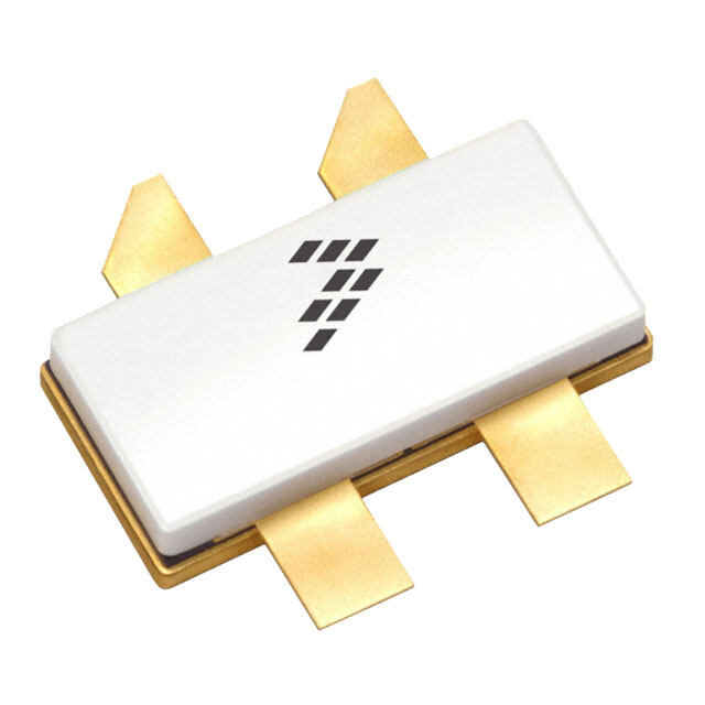
| 供应商器件封装 | 2-CDIP |
| 其它名称 | 568-5104-5 |
| 功率-输出 | 700mW |
| 包装 | 托盘 |
| 噪声系数 | - |
| 增益 | 18.5dB |
| 封装/外壳 | SOT-538A |
| 晶体管类型 | LDMOS |
| 标准包装 | 20 |
| 电压-测试 | 28V |
| 电压-额定 | 65V |
| 电流-测试 | 100mA |
| 频率 | 2.11GHz ~ 2.17GHz |
| 额定电流 | 3.1A |


- 商务部:美国ITC正式对集成电路等产品启动337调查
- 曝三星4nm工艺存在良率问题 高通将骁龙8 Gen1或转产台积电
- 太阳诱电将投资9.5亿元在常州建新厂生产MLCC 预计2023年完工
- 英特尔发布欧洲新工厂建设计划 深化IDM 2.0 战略
- 台积电先进制程称霸业界 有大客户加持明年业绩稳了
- 达到5530亿美元!SIA预计今年全球半导体销售额将创下新高
- 英特尔拟将自动驾驶子公司Mobileye上市 估值或超500亿美元
- 三星加码芯片和SET,合并消费电子和移动部门,撤换高东真等 CEO
- 三星电子宣布重大人事变动 还合并消费电子和移动部门
- 海关总署:前11个月进口集成电路产品价值2.52万亿元 增长14.8%


PDF Datasheet 数据手册内容提取
BLF6G21-10G Power LDMOS transistor Rev. 4 — 1 September 2015 Product data sheet 1. Product profile 1.1 General description 10 W LDMOS power transistor for base station applications at frequencies from HFto2200MHz Table 1. Typical performance I =100mA; T =25C in a common source class-AB production test circuit. Dq case Mode of operation f V P G ACPR DS L(AV) p D (MHz) (V) (W) (dB) (%) (dBc) 2-carrier W-CDMA 2110 to 2170 28 0.7 18.5 15 50[1] 1-carrier W-CDMA 2110 to 2170 28 2 19.3 31 39[1] [1] Test signal: 3GPP; test model 1; 64 DPCH; PAR = 7.5 dB at 0.01 % probability on CCDF per carrier; carrierspacing 5 MHz. CAUTION This device is sensitive to ElectroStatic Discharge (ESD). Therefore care should be taken during transport and handling. 1.2 Features and benefits Typical 2-carrier W-CDMA performance at frequencies of 2110MHz and 2170MHz, asupply voltage of 28 V and an I of 100 mA: Dq Average output power=0.7W Gain=18.5dB Efficiency=15% ACPR=50dBc Typical 1-carrier W-CDMA performance at frequencies of 2110MHz and 2170MHz, asupply voltage of 28 V and an I of 100 mA: Dq Average output power=2W Gain=19.3dB Efficiency=31% ACPR=39dBc Easy power control Integrated ESD protection Excellent ruggedness High efficiency
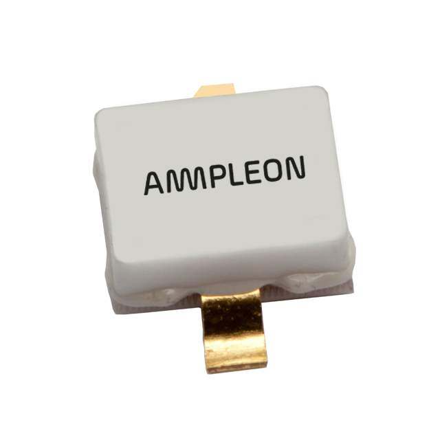
BLF6G21-10G Power LDMOS transistor Excellent thermal stability No internal matching for broadband operation Compliant to Directive 2002/95/EC, regarding Restriction of Hazardous Substances (RoHS) 1.3 Applications RF power amplifiers for GSM, PHS, EDGE, CDMA and W-CDMA base stations and multi carrier applications in the HF to 2200 MHz frequency range Broadcast drivers 2. Pinning information Table 2. Pinning Pin Description Simplified outline Graphic symbol 1 drain 1 1 2 gate 3 source [1] 3 2 3 sym112 2 [1] Connected to flange. 3. Ordering information Table 3. Ordering information Type number Package Name Description Version BLF6G21-10G - ceramic surface-mounted package; 2 leads SOT538A 4. Limiting values Table 4. Limiting values In accordance with the Absolute Maximum Rating System (IEC 60134). Symbol Parameter Conditions Min Max Unit V drain-source voltage - 65 V DS V gate-source voltage 0.5 +13 V GS T storage temperature 65 +150 C stg T junction temperature - 225 C j BLF6G21-10G#4 All information provided in this document is subject to legal disclaimers. © Ampleon The Netherlands B.V. 2015. All rights reserved. Product data sheet Rev. 4 — 1 September 2015 2 of 12
BLF6G21-10G Power LDMOS transistor 5. Thermal characteristics Table 5. Thermal characteristics Symbol Parameter Conditions Typ Unit R thermal resistance from junction to case T = 80 C; P =11W [1] 3.2 K/W th(j-case) case L(AV) [1] Thermal resistance is determined under specified RF operating conditions 6. Characteristics Table 6. Characterist ics T = 25 C unless otherwise specified j Symbol Parameter Conditions Min Typ Max Unit V drain-source breakdown voltage V =0V; I =0.5mA 65 - - V (BR)DSS GS D V gate-source threshold voltage V =10 V; I =18mA 1.4 1.9 2.4 V GS(th) DS D I drain leakage current V =0V; V =28V - - 1.5 A DSS GS DS I drain cut-off current V =V +3.75 V; V =10V - 3.1 - A DSX GS GS(th) DS I gate leakage current V =11V; V =0V - - 150 nA GSS GS DS g forward transconductance V =10V; I =0.9A - 0.5 - S fs DS D R drain-source on-state resistance V =V +3.75 V; I =0.625A - 0.4 - DS(on) GS GS(th) D C feedback capacitance V =0V; V =28V; f=1MHz - 0.5 - pF rs GS DS 7. Application information Table 7. Application information Mode of operation: 2-carrier W-CDMA; PAR 7.5 dB at 0.01 % probability on CCDF; 3GPP testmodel1; 1-64 PDPCH; f = 2112.5 MHz; f = 2117.5 MHz; f = 2162.5 MHz; f =2167.5MHz; 1 2 3 4 RFperformance at V = 28 V; I = 100 mA; T = 25 C; unlessotherwisespecified; in a DS Dq case class-AB production test circuit. Symbol Parameter Conditions Min Typ Max Unit G power gain P = 0.7 W - 18.5 - dB p L(AV) drain efficiency P = 0.7 W - 15 - % D L(AV) ACPR adjacent channel power ratio P = 0.7 W - 50 - dBc L(AV) Table 8. Application information Mode of operation: 1-carrier W-CDMA; PAR 7.5 dB at 0.01 % probability on CCDF; 3GPP testmodel1; 1-64 PDPCH; f = 2112.5 MHz; f = 2167.5 MHz; RFperformance at V =28V; 1 2 DS I =100mA; T = 25 C; unless otherwise specified; in a class-AB production test circuit. Dq case Symbol Parameter Conditions Min Typ Max Unit G power gain P = 2 W 17.3 19.3 - dB p L(AV) drain efficiency P = 2 W 29 31 - % D L(AV) ACPR adjacent channel power ratio P = 2 W - 39 36 dBc L(AV) 7.1 Ruggedness in class-AB operation The BLF6G21-10G is capable of withstanding a load mismatch corresponding to VSWR=10:1 through all phases under the following conditions: V =28V; DS f=2140MHz at P =10W. L BLF6G21-10G#4 All information provided in this document is subject to legal disclaimers. © Ampleon The Netherlands B.V. 2015. All rights reserved. Product data sheet Rev. 4 — 1 September 2015 3 of 12
BLF6G21-10G Power LDMOS transistor 7.2 CW 001aal120 50 RLin (dB) 40 (1) 30 20 (2) (3) 10 0 0 4 8 12 16 PL (W) V = 28 V; I = 100 mA. DS Dq (1) f = 2.11 GHz (2) f = 2.14 GHz (3) f = 2.17 GHz Fig 1. CW input return loss as a function of load power; typicalvalues 001aal121 001aal122 19.5 80 η D Gp (%) (dB) 60 (1) 18.5 (2) (3) 40 17.5 (1) (2) 20 (3) 16.5 0 0 4 8 12 16 0 4 8 12 16 PL (W) PL (W) V = 28 V; I = 100 mA. V = 28 V; I = 100 mA. DS Dq DS Dq (1) f = 2.11 GHz (1) f = 2.11 GHz (2) f = 2.14 GHz (2) f = 2.14 GHz (3) f = 2.17 GHz (3) f = 2.17 GHz Fig 2. CW power gain as a function of load power; Fig 3. CW drain efficiency as a function of typical values loadpower; typical values BLF6G21-10G#4 All information provided in this document is subject to legal disclaimers. © Ampleon The Netherlands B.V. 2015. All rights reserved. Product data sheet Rev. 4 — 1 September 2015 4 of 12
BLF6G21-10G Power LDMOS transistor 7.3 1-carrier W-CDMA 001aal123 50 RLin (dB) 40 (1) 30 20 (2) (3) 10 0 0 1 2 3 4 PL (W) V = 28 V; I = 100 mA. DS Dq (1) f = 2.11 GHz (2) f = 2.14 GHz (3) f = 2.17 GHz Fig 4. 1-carrier W-CDMA input return loss as a function of load power; typicalvalues 001aal124 001aal125 20.0 50 Gp ηD (dB) (%) 19.6 40 19.2 30 (1) (2) (3) (1) 18.8 (2) 20 (3) 18.4 10 18.0 0 0 1 2 3 4 0 1 2 3 4 PL (W) PL (W) V = 28 V; I = 100 mA. V = 28 V; I = 100 mA. DS Dq DS Dq (1) f = 2.11 GHz (1) f = 2.11 GHz (2) f = 2.14 GHz (2) f = 2.14 GHz (3) f = 2.17 GHz (3) f = 2.17 GHz Fig 5. 1-carrier W-CDMA power gain as a function of Fig 6. 1-carrier W-CDMA drain efficiency as a load power; typical values function of loadpower; typical values BLF6G21-10G#4 All information provided in this document is subject to legal disclaimers. © Ampleon The Netherlands B.V. 2015. All rights reserved. Product data sheet Rev. 4 — 1 September 2015 5 of 12
BLF6G21-10G Power LDMOS transistor −30 001aal126 −52 001aal127 ACPR ACPR (dBc) (dBc) −40 −56 (3) (2) (1) −50 −60 (3) (2) (1) −60 −64 0 1 2 3 4 0 1 2 3 4 PL (W) PL (W) V = 28 V; I = 100 mA; carrier spacing 5MHz. V = 28 V; I = 100 mA; carrier spacing 10MHz. DS Dq DS Dq (1) f = 2.11 GHz (1) f = 2.11 GHz (2) f = 2.14 GHz (2) f = 2.14 GHz (3) f = 2.17 GHz (3) f = 2.17 GHz Fig 7. 1-carrier W-CDMA adjacent channel power Fig 8. 1-carrier W-CDMA adjacent channel power ratio as a function of load power; ratio as a function of load power; typicalvalues typicalvalues 7.4 2-carrier W-CDMA 001aal128 40 RLin (dB) (1) 30 20 (2) (3) 10 0 0 0.6 1.2 1.8 PL (W) V = 28 V; I = 100 mA. DS Dq (1) f = 2.11 GHz (2) f = 2.14 GHz (3) f = 2.17 GHz Fig 9. 2-carrier W-CDMA input return loss as a function of load power; typicalvalues BLF6G21-10G#4 All information provided in this document is subject to legal disclaimers. © Ampleon The Netherlands B.V. 2015. All rights reserved. Product data sheet Rev. 4 — 1 September 2015 6 of 12
BLF6G21-10G Power LDMOS transistor 001aal129 001aal130 20.0 30 Gp (dB) η D 19.6 (%) 20 19.2 (1) (1) 18.8 (2) (2) (3) 10 (3) 18.4 18.0 0 0 0.6 1.2 1.8 0 0.6 1.2 1.8 PL (W) PL (W) V = 28 V; I = 100 mA. V = 28 V; I = 100 mA. DS Dq DS Dq (1) f = 2.11 GHz (1) f = 2.11 GHz (2) f = 2.14 GHz (2) f = 2.14 GHz (3) f = 2.17 GHz (3) f = 2.17 GHz Fig 10. 2-carrier W-CDMA power gain as a function of Fig 11. 2-carrier W-CDMA drain efficiency as a load power; typical values function of loadpower; typical values −30 001aal131 −40 001aal132 ACPR ACPR (dBc) (dBc) −45 −40 (3) (3) −50 (2) (2) (1) (1) −50 −55 −60 −60 0 0.6 1.2 1.8 0 0.6 1.2 1.8 PL (W) PL (W) V = 28 V; I = 100 mA; carrier spacing 5MHz. V = 28 V; I = 100 mA; carrier spacing 10MHz. DS Dq DS Dq (1) f = 2.11 GHz (1) f = 2.11 GHz (2) f = 2.14 GHz (2) f = 2.14 GHz (3) f = 2.17 GHz (3) f = 2.17 GHz Fig 12. 2-carrier W-CDMA adjacent channel power Fig 13. 2-carrier W-CDMA adjacent channel power ratio as a function of load power; ratio as a function of load power; typicalvalues typicalvalues BLF6G21-10G#4 All information provided in this document is subject to legal disclaimers. © Ampleon The Netherlands B.V. 2015. All rights reserved. Product data sheet Rev. 4 — 1 September 2015 7 of 12
BLF6G21-10G Power LDMOS transistor 8. Package outline Ceramic surface-mounted package; 2 leads SOT538A D A 3 z2 (4×) z4 (4×) D1 D2 B c 1 Lp L A z1 (4×) H E2 E1 E z3 (4×) 2 b w1 B α Q 0 2.5 5 mm scale Dimensions (mm are the original dimensions) Unit A b c D D1 D2 E E1 E2 H L Lp Q w1 z1 z2 z3 z4 θ max 2.34 1.35 0.23 5.16 4.65 5.16 4.14 3.63 4.14 7.49 2.03 1.02 0.1 0.58 0.25 0.97 0.51 7° mm nom 0.25 min 2.13 1.19 0.18 5.00 4.50 5.00 3.99 3.48 3.99 7.24 1.27 0.51 0.0 0.43 0.18 0.81 0.00 0° sot538a_po Outline References European Issue date version IEC JEDEC JEITA projection 13-02-07 SOT538A 15-04-05 Fig 14. Package outline SOT538A BLF6G21-10G#4 All information provided in this document is subject to legal disclaimers. © Ampleon The Netherlands B.V. 2015. All rights reserved. Product data sheet Rev. 4 — 1 September 2015 8 of 12
BLF6G21-10G Power LDMOS transistor 9. Abbreviations Table 9. Abbreviations Acronym Description 3GPP Third Generation Partnership Project CCDF Complementary Cumulative Distribution Function CDMA Code Division Multiple Access CW Continuous Wave DPCH Dedicated Physical CHannel EDGE Enhanced Data rates for GSM Evolution GSM Global System for Mobile communications HF High Frequency LDMOS Laterally Diffused Metal Oxide Semiconductor PAR Peak-to-Average power Ratio PDPCH transmission Power of the Dedicated Physical CHannel PHS Personal Handy-phone System RF Radio Frequency VSWR Voltage Standing Wave Ratio W-CDMA Wideband Code Division Multiple Access 10. Revision history Table 10. Revision history Document ID Release date Data sheet status Change notice Supersedes BLF6G21-10G#4 20150901 Product data sheet - BLF6G21-10G v.3 Modifications: • The format of this document has been redesigned to comply with the new identity guidelines of Ampleon. • Legal texts have been adapted to the new company name where appropriate. BLF6G21-10G v.3 20130411 Product data sheet - BLF6G21-10G v.2 BLF6G21-10G v.2 20091211 Product data sheet - BLF6G21-10G v.1 BLF6G21-10G v.1 20090511 Objective data sheet - - BLF6G21-10G#4 All information provided in this document is subject to legal disclaimers. © Ampleon The Netherlands B.V. 2015. All rights reserved. Product data sheet Rev. 4 — 1 September 2015 9 of 12
BLF6G21-10G Power LDMOS transistor 11. Legal information 11.1 Data sheet status Document status[1][2] Product status[3] Definition Objective [short] data sheet Development This document contains data from the objective specification for product development. Preliminary [short] data sheet Qualification This document contains data from the preliminary specification. Product [short] data sheet Production This document contains the product specification. [1] Please consult the most recently issued document before initiating or completing a design. [2] The term ‘short data sheet’ is explained in section “Definitions”. [3] The product status of device(s) described in this document may have changed since this document was published and may differ in case of multiple devices. The latest product status information is available on the Internet at URLhttp://www.ampleon.com. 11.2 Definitions Ampleon product can reasonably be expected to result in personal injury, death or severe property or environmental damage. Ampleon and its suppliers accept no liability for inclusion and/or use of Ampleon products in Draft — The document is a draft version only. The content is still under such equipment or applications and therefore such inclusion and/or use is at internal review and subject to formal approval, which may result in the customer’s own risk. modifications or additions. Ampleon does not give any representations or warranties as to the accuracy or completeness of information included herein Applications — Applications that are described herein for any of these and shall have no liability for the consequences of use of such information. products are for illustrative purposes only. Ampleon makes no representation or warranty that such applications will be suitable for the specified use without Short data sheet — A short data sheet is an extract from a full data sheet further testing or modification. with the same product type number(s) and title. A short data sheet is intended for quick reference only and should not be relied upon to contain detailed and Customers are responsible for the design and operation of their applications full information. For detailed and full information see the relevant full data and products using Ampleon products, and Ampleon accepts no liability for sheet, which is available on request via the local Ampleon sales office. In any assistance with applications or customer product design. It is customer’s case of any inconsistency or conflict with the short data sheet, the full data sole responsibility to determine whether the Ampleon product is suitable and sheet shall prevail. fit for the customer’s applications and products planned, as well as for the planned application and use of customer’s third party customer(s). Customers Product specification — The information and data provided in a Product should provide appropriate design and operating safeguards to minimize the data sheet shall define the specification of the product as agreed between risks associated with their applications and products. Ampleon and its customer, unless Ampleon and customer have explicitly Ampleon does not accept any liability related to any default, damage, costs or agreed otherwise in writing. In no event however, shall an agreement be valid problem which is based on any weakness or default in the customer’s in which the Ampleon product is deemed to offer functions and qualities applications or products, or the application or use by customer’s third party beyond those described in the Product data sheet. customer(s). Customer is responsible for doing all necessary testing for the customer’s applications and products using Ampleon products in order to 11.3 Disclaimers avoid a default of the applications and the products or of the application or use by customer’s third party customer(s). Ampleon does not accept any liability in this respect. Limited warranty and liability — Information in this document is believed to be accurate and reliable. However, Ampleon does not give any Limiting values — Stress above one or more limiting values (as defined in representations or warranties, expressed or implied, as to the accuracy or the Absolute Maximum Ratings System of IEC60134) will cause permanent completeness of such information and shall have no liability for the damage to the device. Limiting values are stress ratings only and (proper) consequences of use of such information. Ampleon takes no responsibility for operation of the device at these or any other conditions above those given in the content in this document if provided by an information source outside of the Recommended operating conditions section (if present) or the Ampleon. Characteristics sections of this document is not warranted. Constant or repeated exposure to limiting values will permanently and irreversibly affect In no event shall Ampleon be liable for any indirect, incidental, punitive, the quality and reliability of the device. special or consequential damages (including - without limitation - lost profits, lost savings, business interruption, costs related to the removal or Terms and conditions of commercial sale — Ampleon products are sold replacement of any products or rework charges) whether or not such subject to the general terms and conditions of commercial sale, as published damages are based on tort (including negligence), warranty, breach of at http://www.ampleon.com/terms, unless otherwise agreed in a valid written contract or any other legal theory. individual agreement. In case an individual agreement is concluded only the Notwithstanding any damages that customer might incur for any reason terms and conditions of the respective agreement shall apply. Ampleon whatsoever, Ampleon’ aggregate and cumulative liability towards customer hereby expressly objects to applying the customer’s general terms and for the products described herein shall be limited in accordance with the conditions with regard to the purchase of Ampleon products by customer. Terms and conditions of commercial sale of Ampleon. No offer to sell or license — Nothing in this document may be interpreted or Right to make changes — Ampleon reserves the right to make changes to construed as an offer to sell products that is open for acceptance or the grant, information published in this document, including without limitation conveyance or implication of any license under any copyrights, patents or specifications and product descriptions, at any time and without notice. This other industrial or intellectual property rights. document supersedes and replaces all information supplied prior to the Export control — This document as well as the item(s) described herein publication hereof. may be subject to export control regulations. Export might require a prior Suitability for use — Ampleon products are not designed, authorized or authorization from competent authorities. warranted to be suitable for use in life support, life-critical or safety-critical systems or equipment, nor in applications where failure or malfunction of an BLF6G21-10G#4 All information provided in this document is subject to legal disclaimers. © Ampleon The Netherlands B.V. 2015. All rights reserved. Product data sheet Rev. 4 — 1 September 2015 10 of 12
BLF6G21-10G Power LDMOS transistor Non-automotive qualified products — Unless this data sheet expressly 11.4 Trademarks states that this specific Ampleon product is automotive qualified, the product is not suitable for automotive use. It is neither qualified nor tested in Notice: All referenced brands, product names, service names and trademarks accordance with automotive testing or application requirements. Ampleon are the property of their respective owners. accepts no liability for inclusion and/or use of non-automotive qualified Any reference or use of any ‘NXP’ trademark in this document or in or on the products in automotive equipment or applications. surface of Ampleon products does not result in any claim, liability or In the event that customer uses the product for design-in and use in entitlement vis-à-vis the owner of this trademark. Ampleon is no longer part of automotive applications to automotive specifications and standards, customer the NXP group of companies and any reference to or use of the ‘NXP’ (a) shall use the product without Ampleon’ warranty of the product for such trademarks will be replaced by reference to or use of Ampleon’s own Any automotive applications, use and specifications, and (b) whenever customer reference or use of any ‘NXP’ trademark in this document or in or on the uses the product for automotive applications beyond Ampleon’ specifications surface of Ampleon products does not result in any claim, liability or such use shall be solely at customer’s own risk, and (c) customer fully entitlement vis-à-vis the owner of this trademark. Ampleon is no longer part of indemnifies Ampleon for any liability, damages or failed product claims the NXP group of companies and any reference to or use of the ‘NXP’ resulting from customer design and use of the product for automotive trademarks will be replaced by reference to or use of Ampleon’s own applications beyond Ampleon’ standard warranty and Ampleon’ product trademarks. specifications. Translations — A non-English (translated) version of a document is for reference only. The English version shall prevail in case of any discrepancy between the translated and English versions. 12. Contact information For more information, please visit: For sales office addresses, please visit: http://www.ampleon.com http://www.ampleon.com/sales BLF6G21-10G#4 All information provided in this document is subject to legal disclaimers. © Ampleon The Netherlands B.V. 2015. All rights reserved. Product data sheet Rev. 4 — 1 September 2015 11 of 12
BLF6G21-10G Power LDMOS transistor 13. Contents 1 Product profile. . . . . . . . . . . . . . . . . . . . . . . . . . 1 1.1 General description . . . . . . . . . . . . . . . . . . . . . 1 1.2 Features and benefits. . . . . . . . . . . . . . . . . . . . 1 1.3 Applications . . . . . . . . . . . . . . . . . . . . . . . . . . . 2 2 Pinning information. . . . . . . . . . . . . . . . . . . . . . 2 3 Ordering information. . . . . . . . . . . . . . . . . . . . . 2 4 Limiting values. . . . . . . . . . . . . . . . . . . . . . . . . . 2 5 Thermal characteristics . . . . . . . . . . . . . . . . . . 3 6 Characteristics. . . . . . . . . . . . . . . . . . . . . . . . . . 3 7 Application information. . . . . . . . . . . . . . . . . . . 3 7.1 Ruggedness in class-AB operation . . . . . . . . . 3 7.2 CW . . . . . . . . . . . . . . . . . . . . . . . . . . . . . . . . . . 4 7.3 1-carrier W-CDMA . . . . . . . . . . . . . . . . . . . . . . 5 7.4 2-carrier W-CDMA . . . . . . . . . . . . . . . . . . . . . . 6 8 Package outline. . . . . . . . . . . . . . . . . . . . . . . . . 8 9 Abbreviations. . . . . . . . . . . . . . . . . . . . . . . . . . . 9 10 Revision history. . . . . . . . . . . . . . . . . . . . . . . . . 9 11 Legal information. . . . . . . . . . . . . . . . . . . . . . . 10 11.1 Data sheet status . . . . . . . . . . . . . . . . . . . . . . 10 11.2 Definitions. . . . . . . . . . . . . . . . . . . . . . . . . . . . 10 11.3 Disclaimers. . . . . . . . . . . . . . . . . . . . . . . . . . . 10 11.4 Trademarks. . . . . . . . . . . . . . . . . . . . . . . . . . . 11 12 Contact information. . . . . . . . . . . . . . . . . . . . . 11 13 Contents. . . . . . . . . . . . . . . . . . . . . . . . . . . . . . 12 Please be aware that important notices concerning this document and the product(s) described herein, have been included in section ‘Legal information’. © Ampleon The Netherlands B.V. 2015. All rights reserved. For more information, please visit: http://www.ampleon.com For sales office addresses, please visit: http://www.ampleon.com/sales Date of release: 1 September 2015 Document identifier: BLF6G21-10G#4