ICGOO在线商城 > 分立半导体产品 > 晶体管 - FET,MOSFET - 射频 > CGH55015F2
 Datasheet下载
- 型号: CGH55015F2
- 制造商: Cree
- 库位|库存: xxxx|xxxx
- 要求:
| 数量阶梯 | 香港交货 | 国内含税 |
| +xxxx | $xxxx | ¥xxxx |
查看当月历史价格
查看今年历史价格
CGH55015F2产品简介:
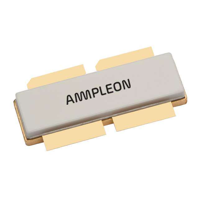
ICGOO电子元器件商城为您提供CGH55015F2由Cree设计生产,在icgoo商城现货销售,并且可以通过原厂、代理商等渠道进行代购。 CGH55015F2价格参考¥642.07-¥642.16。CreeCGH55015F2封装/规格:晶体管 - FET,MOSFET - 射频, 射频 Mosfet HEMT 28V 200mA 5.65GHz 12dB 12.5W 440166。您可以下载CGH55015F2参考资料、Datasheet数据手册功能说明书,资料中有CGH55015F2 详细功能的应用电路图电压和使用方法及教程。
型号为CGH55015F2的射频MOSFET晶体管,由Wolfspeed(原Cree)生产,主要应用于高频、高功率的射频系统中。该器件基于氮化镓(GaN)技术,具备高效能和高可靠性。

其典型应用场景包括:

1. 无线通信基础设施:如4G/5G基站、宏蜂窝和微蜂窝基站中的射频功率放大器模块,用于提高信号传输效率与覆盖范围。
2. 广播系统:用于FM广播、电视广播等发射设备中的高功率射频放大电路。
3. 工业与医疗射频设备:如射频加热、激光器驱动、医学成像设备中的功率控制单元。
4. 雷达系统:适用于军用或民用雷达中的发射机部分,提供高线性度与输出功率。
5. 测试与测量仪器:在射频信号发生器、功率放大器等测试设备中作为核心功率器件使用。

CGH55015F2因其高效率、宽带宽及良好的热性能,适合要求严苛的射频应用环境。
| 参数 | 数值 |
| 产品目录 | |
| 描述 | FET RF HEMT 5.65GHZ 84V 440166 |
| 产品分类 | RF FET |
| 品牌 | Cree Inc |
| 数据手册 | |
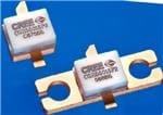
| 产品图片 |
|
| 产品型号 | CGH55015F2 |
| rohs | 无铅 / 符合限制有害物质指令(RoHS)规范要求 |
| 产品系列 | - |
| 供应商器件封装 | 440166 |
| 功率-输出 | 12.5W |
| 包装 | 管件 |
| 噪声系数 | - |
| 增益 | 12dB |
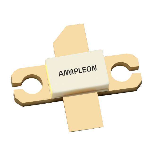
| 封装/外壳 | 440166 |
| 晶体管类型 | HEMT |
| 标准包装 | 58 |
| 电压-测试 | 28V |
| 电压-额定 | 84V |
| 电流-测试 | 200mA |
| 频率 | 5.65GHz |
| 额定电流 | - |


- 商务部:美国ITC正式对集成电路等产品启动337调查
- 曝三星4nm工艺存在良率问题 高通将骁龙8 Gen1或转产台积电
- 太阳诱电将投资9.5亿元在常州建新厂生产MLCC 预计2023年完工
- 英特尔发布欧洲新工厂建设计划 深化IDM 2.0 战略
- 台积电先进制程称霸业界 有大客户加持明年业绩稳了
- 达到5530亿美元!SIA预计今年全球半导体销售额将创下新高
- 英特尔拟将自动驾驶子公司Mobileye上市 估值或超500亿美元
- 三星加码芯片和SET,合并消费电子和移动部门,撤换高东真等 CEO
- 三星电子宣布重大人事变动 还合并消费电子和移动部门
- 海关总署:前11个月进口集成电路产品价值2.52万亿元 增长14.8%


PDF Datasheet 数据手册内容提取
CGH55015F2 / CGH55015P2 10 W, C-band, Unmatched, GaN HEMT Cree’s CGH55015F2/CGH55015P2 is a gallium nitride (GaN) high electron mobility transistor (HEMT) designed specifically for high efficiency, high gain and wide bandwidth capabilities, which makes the CGH55015F2/CGH55015P2 ideal for C-band pulsed or CW saturated amplifiers. The transistor is available in both screw- down, flange and solder-down, pill packages. Based on appropriate external match adjustment, the CGH55015F2/CGH55015P2 is suitable for applications up to 6 GHz. PPNa:c CkGagHe5 T5y0p1e5:P 424 0&1 C9G6H &5 54041051F626 FEATURES APPLICATIONS • 4.5 to 6.0 GHz Operation • 2-Way Private Radio • 12 dB Small Signal Gain at 5.65 GHz • Broadband Amplifiers • 13 W typical P • Cellular Infrastructure SAT • 60 % Efficiency at P • Test Instrumentation SAT • 28 V Operation • Class A, AB Amplifiers for Drivers and Gain Blocks 5 1 0 2 y a M – 0 .4 v e R Subject to change without notice. 1 www.cree.com/wireless
Absolute Maximum Ratings (not simultaneous) at 25˚C Case Temperature Parameter Symbol Rating Units Conditions Drain-Source Voltage V 84 Volts 25˚C DSS Gate-to-Source Voltage V -10, +2 Volts 25˚C GS Storage Temperature T -65, +150 ˚C STG Operating Junction Temperature T 225 ˚C J Maximum Forward Gate Current I 4.0 mA 25˚C GMAX Maximum Drain Current1 I 1.5 A 25˚C DMAX Soldering Temperature2 T 245 ˚C S Screw Torque τ 60 in-oz Thermal Resistance, Junction to Case3 R 8.0 ˚C/W 85˚C θJC Case Operating Temperature3,4 T -40, +150 ˚C 30 seconds C Note: 1 Current limit for long term, reliable operation. 2 Refer to the Application Note on soldering at www.cree.com/RF/Document-Library 3 Measured for the CGH55015 at P = 14W. DISS 4 See also, the Power Dissipation De-rating Curve on Page 5. Electrical Characteristics (T = 25˚C) C Characteristics Symbol Min. Typ. Max. Units Conditions DC Characteristics1 Gate Threshold Voltage V -3.8 -3.0 -2.3 V V = 10 V, I = 3.6 mA GS(th) DC DS D Gate Quiescent Voltage V – -2.7 – V V = 28 V, I = 200 mA GS(Q) DC DS D Saturated Drain Current I 2.9 3.5 – A V = 6.0 V, V = 2.0 V DS DS GS Drain-Source Breakdown Voltage V 120 – – V V = -8 V, I = 3.6 mA BR DC GS D RF Characteristics2 (T = 25˚C, F = 5.65 GHz unless otherwise noted) C 0 Small Signal Gain G 10 12 – dB V = 28 V, I = 200 mA SS DD DQ Power Output3 P 10 12.5 – W V = 28 V, I = 200 mA SAT DD DQ Drain Efficiency4 η 50 60 – % V = 28 V, I = 200 mA, P = 10 W DD DQ OUT No damage at all phase angles, Output Mismatch Stress VSWR – – 10 : 1 Y V = 28 V, I = 200 mA, DD DQ P = 10 W CW OUT Dynamic Characteristics Input Capacitance C – 4.5 – pF V = 28 V, V = -8 V, f = 1 MHz GS DS gs Output Capacitance C – 1.3 – pF V = 28 V, V = -8 V, f = 1 MHz DS DS gs Feedback Capacitance C – 0.2 – pF V = 28 V, V = -8 V, f = 1 MHz GD DS gs Notes: 1 Measured on wafer prior to packaging. 2 Measured in CGH55015-AMP 3 P is defined as I = 0.36 mA. SAT G 4 Drain Efficiency = P / P OUT DC Cree, Inc. 4600 Silicon Drive Copyright © 2008-2015 Cree, Inc. All rights reserved. The information in this document is subject to change without notice. Cree and the Cree logo are Durham, North Carolina, USA 27703 registered trademarks of Cree, Inc. USA Tel: +1.919.313.5300 Fax: +1.919.869.2733 2 CGH55015F2_P2 Rev 4.0 www.cree.com/wireless
Typical Performance Small Signal S-Parameters vs Frequency of CGH55015F2 and CGH55015P2 in the CGH55015-AMP Gainand VInp u=t 2R8e tVru, nILo =s s2v0s0F mreAquencyof CGH5D5D015F Vdd=DQ28V,Idq=115mA 14 2 13 1 12 0 11 -1 10 -2 9 -3 B)B) 8 -4 B)B) dd dd (( 7 -5 (( 11 11 22 11 SS 6 -6 SS 5 -7 S21 S11 4 -8 3 -9 2 -10 1 -11 0 -12 5.2 5.3 5.4 5.5 5.6 5.7 5.8 5.9 6.0 6.1 Frequency(GHz) Drain Efficiency, Power and Gain vs Frequency of the CGH55015F2 and CGH55015P2 in the CGH55015-AMP CGH55015-GaNHEMTC-BandPerformance V = 28 V, I = 200 mA DrainEfficiencDyD,Power,anDQdGainvsFrequency 70 B)B)60 dd (( nn aiai GG50 m),m), BB dd at(at(40 ss PP %),%), ((30 Gain(dB) yy cc nn Psat(dBm) ee cici EffiEffi20 DrainEfficiency(%) nn aiai DrDr10 0 5.3 5.4 5.5 5.6 5.7 5.8 5.9 6 Frequency(GHz) Cree, Inc. 4600 Silicon Drive Copyright © 2008-2015 Cree, Inc. All rights reserved. The information in this document is subject to change without notice. Cree and the Cree logo are Durham, North Carolina, USA 27703 registered trademarks of Cree, Inc. USA Tel: +1.919.313.5300 Fax: +1.919.869.2733 3 CGH55015F2_P2 Rev 4.0 www.cree.com/wireless
Typical Performance Simulated Maximum Available Gain and K Factor of the CGH55015F2/CGH55015P2 V = 28 V, I = 200 mA DD DQ ) B r d o G ( act A F M K Typical Noise Performance Simulated Minimum Noise Figure and Noise Resistance vs Frequency of the CGH55015F2/CGH55015P2 V = 28 V, I = 200 mA DD DQ ) B ) d s ( m e h ur O g ( Fi ce e n s a oi st N si m e R mu e s ni oi Mi N Electrostatic Discharge (ESD) Classifications Parameter Symbol Class Test Methodology Human Body Model HBM 1A > 250 V JEDEC JESD22 A114-D Charge Device Model CDM 1 < 200 V JEDEC JESD22 C101-C Cree, Inc. 4600 Silicon Drive Copyright © 2008-2015 Cree, Inc. All rights reserved. The information in this document is subject to change without notice. Cree and the Cree logo are Durham, North Carolina, USA 27703 registered trademarks of Cree, Inc. USA Tel: +1.919.313.5300 Fax: +1.919.869.2733 4 CGH55015F2_P2 Rev 4.0 www.cree.com/wireless
Source and Load Impedances D Z Source Z Load G S Frequency (MHz) Z Source Z Load 5500 8.7 – j30.2 21.6 – j4.7 5650 10.2 – j26.9 24.2 - j5.5 5800 12.3 – j24.3 26.5 - j7.5 Note 1. V = 28V, I = 200 mA in the 440166 package. DD DQ Note 2. Impedances are extracted from the CGH55015-AMP demonstration amplifier and are not source and load pull data derived from the transistor. CGH55015F2 and CGH55015P2 Power Dissipation De-rating Curve CGH40010FCWPowerDissipationDe-ratingCurve 16 14 12 W)W) (( nn oo 10 atiati pp sisi DisDis 8 erer Note1 ww oo 6 PP 4 2 0 0 25 50 75 100 125 150 175 200 225 250 MaximumCaseTemperature(°C) Note 1. Area exceeds Maximum Case Operating Temperature (See Page 2). Cree, Inc. 4600 Silicon Drive Copyright © 2008-2015 Cree, Inc. All rights reserved. The information in this document is subject to change without notice. Cree and the Cree logo are Durham, North Carolina, USA 27703 registered trademarks of Cree, Inc. USA Tel: +1.919.313.5300 Fax: +1.919.869.2733 5 CGH55015F2_P2 Rev 4.0 www.cree.com/wireless
CGH55015-AMP Demonstration Amplifier Circuit Bill of Materials Designator Description Qty C1 CAP, 1.2pF, +/-0.1 pF, 0603, ATC 600S 1 C2 CAP, 0.3pF, +/-0.05 pF, 0402, ATC 600L 1 C9 CAP, 0.5pF,+/-0.05pF, 0603, ATC 600S 1 C4,C11 CAP, 18pF, +/-5%, 0603, ATC 600S 2 C5,C12 CAP, 39pF +/-5%, 0603, ATC 600S 2 C6,C13 CAP, CER, 180pF, 50V, +/-5%, C0G, 0603 2 C7,C14 CAP, CER, 0.1UF, 50V, +/-10%, X7R, 0805 2 C8 CAP, 10UF, 16V, SMT, TANTALUM 1 C15 CAP, 1.0UF ±10%, 100V, 1210, X7R 1 C16 CAP, 33UF, 100V, ELECT, FK, SMD 1 R1 RES, 1/16W, 0603, 1%, 562 OHMS 1 R2 RES, 1/16W, 0603, 1%, 22 OHMS 1 J1 HEADER RT> PLZ .1 CEN LK 5 POS 1 J3,J4 CONN, SMA, FLANGE 2 - PCB, RO4350B, Er = 3.48, h = 20 mil 1 - CGH55015 1 CGH55015-AMP Demonstration Amplifier Circuit Cree, Inc. 4600 Silicon Drive Copyright © 2008-2015 Cree, Inc. All rights reserved. The information in this document is subject to change without notice. Cree and the Cree logo are Durham, North Carolina, USA 27703 registered trademarks of Cree, Inc. USA Tel: +1.919.313.5300 Fax: +1.919.869.2733 6 CGH55015F2_P2 Rev 4.0 www.cree.com/wireless
CGH55015-AMP Demonstration Amplifier Circuit Schematic CGH55015-AMP Demonstration Amplifier Circuit Outline Cree, Inc. 4600 Silicon Drive Copyright © 2008-2015 Cree, Inc. All rights reserved. The information in this document is subject to change without notice. Cree and the Cree logo are Durham, North Carolina, USA 27703 registered trademarks of Cree, Inc. USA Tel: +1.919.313.5300 Fax: +1.919.869.2733 7 CGH55015F2_P2 Rev 4.0 www.cree.com/wireless
Typical Package S-Parameters for CGH55015F2 / CGH55015P2 (Small Signal, V = 28 V, I = 200 mA, angle in degrees) DS DQ Frequency Mag S11 Ang S11 Mag S21 Ang S21 Mag S12 Ang S12 Mag S22 Ang S22 500 MHz 0.911 -130.86 18.44 105.32 0.022 19.38 0.302 -113.00 600 MHz 0.906 -139.86 15.82 99.40 0.023 14.28 0.299 -120.56 700 MHz 0.902 -146.89 13.81 94.44 0.023 10.15 0.298 -126.20 800 MHz 0.900 -152.58 12.23 90.14 0.023 6.68 0.299 -130.51 900 MHz 0.898 -157.33 10.97 86.29 0.023 3.69 0.302 -133.91 1.0 GHz 0.897 -161.38 9.93 82.79 0.023 1.03 0.305 -136.65 1.1 GHz 0.896 -164.92 9.06 79.53 0.023 -1.36 0.309 -138.93 1.2 GHz 0.895 -168.07 8.33 76.47 0.023 -3.55 0.314 -140.86 1.3 GHz 0.895 -170.92 7.71 73.56 0.023 -5.58 0.320 -142.55 1.4 GHz 0.895 -173.52 7.17 70.77 0.023 -7.47 0.326 -144.06 1.5 GHz 0.894 -175.93 6.70 68.08 0.023 -9.25 0.332 -145.44 1.6 GHz 0.894 -178.19 6.29 65.47 0.023 -10.93 0.338 -146.73 1.7 GHz 0.894 179.68 5.92 62.93 0.023 -12.52 0.345 -147.96 1.8 GHz 0.894 177.66 5.60 60.44 0.023 -14.04 0.351 -149.13 1.9 GHz 0.894 175.72 5.31 58.01 0.022 -15.49 0.358 -150.28 2.0 GHz 0.894 173.85 5.04 55.62 0.022 -16.88 0.365 -151.42 2.1 GHz 0.895 172.04 4.80 53.26 0.022 -18.21 0.372 -152.54 2.2 GHz 0.895 170.28 4.59 50.93 0.022 -19.48 0.379 -153.66 2.3 GHz 0.895 168.57 4.39 48.64 0.022 -20.69 0.386 -154.78 2.4 GHz 0.895 166.88 4.21 46.37 0.021 -21.85 0.393 -155.92 2.5 GHz 0.895 165.22 4.04 44.11 0.021 -22.96 0.400 -157.06 2.6 GHz 0.895 163.58 3.88 41.88 0.021 -24.02 0.407 -158.21 2.7 GHz 0.895 161.97 3.74 39.67 0.021 -25.02 0.413 -159.37 2.8 GHz 0.896 160.36 3.61 37.47 0.020 -25.97 0.420 -160.55 2.9 GHz 0.896 158.76 3.49 35.28 0.020 -26.87 0.426 -161.75 3.0 GHz 0.896 157.17 3.37 33.11 0.020 -27.72 0.433 -162.96 3.2 GHz 0.896 153.99 3.17 28.79 0.019 -29.24 0.445 -165.43 3.4 GHz 0.896 150.81 2.99 24.49 0.019 -30.53 0.456 -167.97 3.6 GHz 0.897 147.59 2.83 20.21 0.018 -31.57 0.467 -170.58 3.8 GHz 0.897 144.34 2.69 15.94 0.018 -32.35 0.477 -173.26 4.0 GHz 0.897 141.03 2.56 11.67 0.017 -32.86 0.487 -176.01 4.2 GHz 0.897 137.66 2.45 7.39 0.017 -33.08 0.496 -178.84 4.4 GHz 0.897 134.20 2.35 3.09 0.017 -33.02 0.504 178.25 4.6 GHz 0.897 130.65 2.26 -1.24 0.016 -32.67 0.511 175.25 4.8 GHz 0.897 127.01 2.18 -5.61 0.016 -32.06 0.517 172.16 5.0 GHz 0.896 123.25 2.11 -10.03 0.016 -31.23 0.523 168.97 5.2 GHz 0.896 119.37 2.04 -14.50 0.016 -30.22 0.528 165.68 5.4 GHz 0.896 115.36 1.98 -19.04 0.016 -29.11 0.532 162.26 5.6 GHz 0.896 111.21 1.92 -23.65 0.016 -27.99 0.536 158.72 5.8 GHz 0.895 106.92 1.87 -28.34 0.017 -26.98 0.539 155.04 6.0 GHz 0.895 102.47 1.83 -33.12 0.017 -26.15 0.541 151.21 To download the s-parameters in s2p format, go to the CGH55015F2/P2 Product Page, click on the documentation tab. Cree, Inc. 4600 Silicon Drive Copyright © 2008-2015 Cree, Inc. All rights reserved. The information in this document is subject to change without notice. Cree and the Cree logo are Durham, North Carolina, USA 27703 registered trademarks of Cree, Inc. USA Tel: +1.919.313.5300 Fax: +1.919.869.2733 8 CGH55015F2_P2 Rev 4.0 www.cree.com/wireless
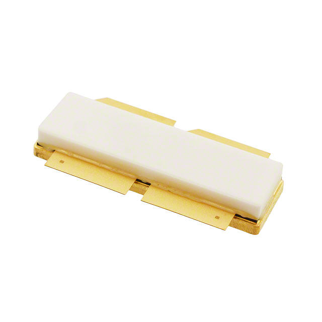
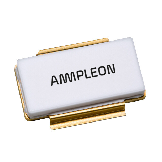
Product Dimensions CGH55015F2 (Package Type — 440166) Product Dimensions CGH55015P2 (Package Type — 440196) Cree, Inc. 4600 Silicon Drive Copyright © 2008-2015 Cree, Inc. All rights reserved. The information in this document is subject to change without notice. Cree and the Cree logo are Durham, North Carolina, USA 27703 registered trademarks of Cree, Inc. USA Tel: +1.919.313.5300 Fax: +1.919.869.2733 9 CGH55015F2_P2 Rev 4.0 www.cree.com/wireless
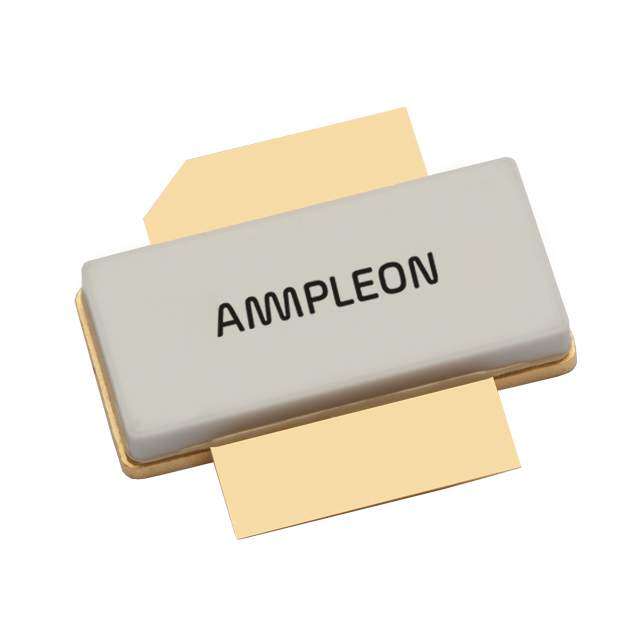
Product Ordering Information Order Number Description Unit of Measure Image CGH55015F2 GaN HEMT Each 2.709 in CGH55015P2 GaN HEMT Each 4.584 in CGH55015-TB Test board without GaN HEMT Each CGH55015-AMP Test board with GaN HEMT installed Each Cree, Inc. 4600 Silicon Drive Copyright © 2008-2015 Cree, Inc. All rights reserved. The information in this document is subject to change without notice. Cree and the Cree logo are Durham, North Carolina, USA 27703 registered trademarks of Cree, Inc. USA Tel: +1.919.313.5300 Fax: +1.919.869.2733 10 CGH55015F2_P2 Rev 4.0 www.cree.com/wireless
Disclaimer Specifications are subject to change without notice. Cree, Inc. believes the information contained within this data sheet to be accurate and reliable. However, no responsibility is assumed by Cree for any infringement of patents or other rights of third parties which may result from its use. No license is granted by implication or otherwise under any patent or patent rights of Cree. Cree makes no warranty, representation or guarantee regarding the suitability of its products for any particular purpose. “Typical” parameters are the average values expected by Cree in large quantities and are provided for information purposes only. These values can and do vary in different applications and actual performance can vary over time. All operating parameters should be validated by customer’s technical experts for each application. Cree products are not designed, intended or authorized for use as components in applications intended for surgical implant into the body or to support or sustain life, in applications in which the failure of the Cree product could result in personal injury or death or in applications for planning, construction, maintenance or direct operation of a nuclear facility. For more information, please contact: Cree, Inc. 4600 Silicon Drive Durham, North Carolina, USA 27703 www.cree.com/RF Sarah Miller Marketing Cree, RF Components 1.919.407.5302 Ryan Baker Marketing & Sales Cree, Wireless Devices 1.919.287.7816 Tom Dekker Sales Director Cree, Wireless Devices 1.919.313.5639 Cree, Inc. 4600 Silicon Drive Copyright © 2008-2015 Cree, Inc. All rights reserved. The information in this document is subject to change without notice. Cree and the Cree logo are Durham, North Carolina, USA 27703 registered trademarks of Cree, Inc. USA Tel: +1.919.313.5300 Fax: +1.919.869.2733 11 CGH55015F2_P2 Rev 4.0 www.cree.com/wireless
Mouser Electronics Authorized Distributor Click to View Pricing, Inventory, Delivery & Lifecycle Information: C ree, Inc.: CGH55015F2