ICGOO在线商城 > 分立半导体产品 > 晶体管 - FET,MOSFET - 单 > AON7406

 Datasheet下载
- 型号: AON7406
- 制造商: ALPHA&OMEGA
- 库位|库存: xxxx|xxxx
- 要求:
| 数量阶梯 | 香港交货 | 国内含税 |
| +xxxx | $xxxx | ¥xxxx |
查看当月历史价格
查看今年历史价格
AON7406产品简介:
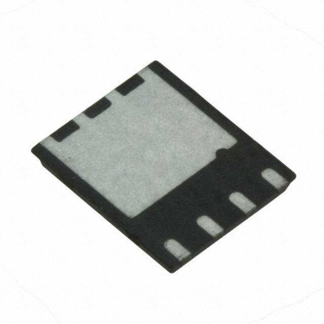
ICGOO电子元器件商城为您提供AON7406由ALPHA&OMEGA设计生产,在icgoo商城现货销售,并且可以通过原厂、代理商等渠道进行代购。 AON7406价格参考。ALPHA&OMEGAAON7406封装/规格:晶体管 - FET,MOSFET - 单, 表面贴装 N 沟道 30V 9A(Ta),25A(Tc) 3.1W(Ta),15.5W(Tc) 8-DFN(3x3)。您可以下载AON7406参考资料、Datasheet数据手册功能说明书,资料中有AON7406 详细功能的应用电路图电压和使用方法及教程。
AON7406是Alpha & Omega Semiconductor Inc.生产的一款N沟道MOSFET,属于单MOSFET晶体管产品系列。该器件具有低导通电阻(RDS(on))、高效率和优异的开关性能,广泛应用于对能效和空间要求较高的电子设备中。

其典型应用场景包括:便携式电子产品(如智能手机、平板电脑)中的电源管理与负载开关,用于电池供电系统的高效能量控制;在DC-DC转换器中作为同步整流或开关元件,提升转换效率;适用于电机驱动电路,如微型马达或风扇控制;还可用于热插拔电路、LED驱动及各类电源开关模块。

AON7406采用小型封装(如DFN3x3或SO-8),适合高密度PCB布局,有助于缩小整体设计体积。其良好的热性能和可靠性也使其适用于工业控制、消费类电器和通信设备等环境。总体而言,AON7406是一款高性能、低成本的功率MOSFET,特别适合中低功率开关应用场合。
| 参数 | 数值 |
| 产品目录 | |
| 描述 | MOSFET N-CH 30V 9A 8-DFN |
| 产品分类 | FET - 单 |
| FET功能 | 逻辑电平门 |
| FET类型 | MOSFET N 通道,金属氧化物 |
| 品牌 | Alpha & Omega Semiconductor Inc |
| 数据手册 | |
| 产品图片 |
|
| 产品型号 | AON7406 |
| PCN组件/产地 | |
| rohs | 无铅 / 符合限制有害物质指令(RoHS)规范要求 |
| 产品系列 | - |
| 不同Id时的Vgs(th)(最大值) | 2.4V @ 250µA |
| 不同Vds时的输入电容(Ciss) | 888pF @ 15V |
| 不同Vgs时的栅极电荷(Qg) | 18nC @ 10V |
| 不同 Id、Vgs时的 RdsOn(最大值) | 17 毫欧 @ 9A,10V |
| 供应商器件封装 | 8-DFN(3x3) |
| 其它名称 | 785-1137-1 |
| 其它图纸 |
|
| 功率-最大值 | 3.1W |
| 包装 | 剪切带 (CT) |
| 安装类型 | 表面贴装 |
| 封装/外壳 | 8-PowerVDFN |
| 标准包装 | 1 |
| 漏源极电压(Vdss) | 30V |
| 电流-连续漏极(Id)(25°C时) | 9A (Ta), 25A (Tc) |


PDF Datasheet 数据手册内容提取
AON7406 30V N-Channel MOSFET General Description Product Summary • The AON7406 uses advanced trench technology and VDS 30V design to provide excellent RDS(ON) with low gate charge. ID (at VGS=10V) 25A This device is suitable for use in SMPS and general R (at V =10V) < 17mW DS(ON) GS purpose applications. R (at V =4.5V) < 23mW DS(ON) GS Typical ESD protection HBM Class 2 • RoHS and Halogen-Free Compliant 100% UIS Tested 100% R Tested g DFN 3x3A D Top View Bottom View Top View S D S D S D G G D Pin 1 S Pin 1 Absolute Maximum Ratings T =25°C unless otherwise noted A Parameter Symbol Maximum Units DDrraaiinn--SSoouurrccee VVoollttaaggee VV 3300 VV DDSS Gate-Source Voltage V ±20 V GS Continuous Drain TC=25°C I 25 Current T =100°C D 15 A C Pulsed Drain Current C I 50 DM Continuous Drain TA=25°C I 9 A Current T =70°C DSM 7 A Avalanche Current C I , I 19 A AS AR Avalanche energy L=0.1mH C E , E 18 mJ AS AR T =25°C 15.5 C P W Power Dissipation B T =100°C D 6 C T =25°C 3.1 A P W Power Dissipation A T =70°C DSM 2 A Junction and Storage Temperature Range T, T -55 to 150 °C J STG Thermal Characteristics Parameter Symbol Typ Max Units Maximum Junction-to-Ambient A t ≤ 10s 30 40 °C/W Maximum Junction-to-Ambient A D Steady-State RqJA 60 75 °C/W Maximum Junction-to-Case Steady-State RqJC 6.6 8 °C/W Rev.6.0: July 2013 www.aosmd.com Page 1 of 6
AON7406 Electrical Characteristics (T =25°C unless otherwise noted) J Symbol Parameter Conditions Min Typ Max Units STATIC PARAMETERS BV Drain-Source Breakdown Voltage I =250m A, V =0V 30 V DSS D GS V =30V, V =0V 1 I Zero Gate Voltage Drain Current DS GS m A DSS T=55°C 5 J I Gate-Body leakage current V =0V, V = ±16V 10 m A GSS DS GS V Gate Threshold Voltage V =V I =250m A 1.2 1.8 2.4 V GS(th) DS GS D I On state drain current V =10V, V =5V 50 A D(ON) GS DS V =10V, I =9A 14 17 GS D mW R Static Drain-Source On-Resistance T=125°C 20 24 DS(ON) J V =4.5V, I =8A 18 23 mW GS D g Forward Transconductance V =5V, I =9A 40 S FS DS D V Diode Forward Voltage I =1A,V =0V 0.75 1 V SD S GS I Maximum Body-Diode Continuous Current 15 A S DYNAMIC PARAMETERS C Input Capacitance 600 740 888 pF iss C Output Capacitance V =0V, V =15V, f=1MHz 77 110 145 pF oss GS DS C Reverse Transfer Capacitance 50 82 115 pF rss R Gate resistance V =0V, V =0V, f=1MHz 0.5 1.1 1.7 W g GS DS SWITCHING PARAMETERS Q (10V) Total Gate Charge 12 15 18 nC g Q (4.5V) Total Gate Charge 6 7.5 9 nC g V =10V, V =15V, I =9A GS DS D Q Gate Source Charge 2.5 nC gs Q Gate Drain Charge 3 nC gd t Turn-On DelayTime 5 ns D(on) tt TTuurrnn--OOnn RRiissee TTiimmee VV ==1100VV,, VV ==1155VV,, RR ==11..6677WW ,, 33..55 nnss r GS DS L t Turn-Off DelayTime R =3W 19 ns D(off) GEN t Turn-Off Fall Time 3.5 ns f trr Body Diode Reverse Recovery Time IF=9A, dI/dt=500A/m s 6 8 10 ns Qrr Body Diode Reverse Recovery Charge IF=9A, dI/dt=500A/m s 14 18 22 nC A. The value of RqJAis measured with the device mounted on 1in2FR-4 board with 2oz. Copper, in a still air environment with TA=25°C. The Power dissipation PDSMis based on R qJA t ≤10s value and the maximum allowed junction temperature of 150°C. The value in any given application depends on the user's specific board design. B. The power dissipation P is based on T =150°C, using junction-to-case thermal resistance, and is more useful in setting the upper D J(MAX) dissipation limit for cases where additional heatsinking is used. C. Repetitive rating, pulse width limited by junction temperature T =150°C. Ratings are based on low frequency and duty cycles to keep J(MAX) initial T =25°C. J D. The RqJAis the sum of the thermal impedence from junction to case RqJCand case to ambient. E. The static characteristics in Figures 1 to 6 are obtained using <300m s pulses, duty cycle 0.5% max. F. These curves are based on the junction-to-case thermal impedence which is measured with the device mounted to a large heatsink, assuming a maximum junction temperature of T =150°C. The SOA curve provides a single pulse rating. J(MAX) G. The maximum current rating is package limited. H. These tests are performed with the device mounted on 1 in2FR-4 board with 2oz. Copper, in a still air environment with T =25°C. A THIS PRODUCT HAS BEEN DESIGNED AND QUALIFIED FOR THE CONSUMER MARKET. APPLICATIONS OR USES AS CRITICAL COMPONENTS IN LIFE SUPPORT DEVICES OR SYSTEMS ARE NOT AUTHORIZED. AOS DOES NOT ASSUME ANY LIABILITY ARISING OUT OF SUCH APPLICATIONS OR USES OF ITS PRODUCTS. AOS RESERVES THE RIGHT TO IMPROVE PRODUCT DESIGN, FUNCTIONS AND RELIABILITY WITHOUT NOTICE. Rev.6.0: July 2013 www.aosmd.com Page 2 of 6
AON7406 TYPICAL ELECTRICAL AND THERMAL CHARACTERISTICS 30 30 10V V =5V 25 4V 25 DS 5V 20 20 3V A) 15 A) 15 I(D I(D 10 10 125°C 5 VGS=2.5V 5 25°C 0 0 0 1 2 3 4 5 1 1.5 2 2.5 3 3.5 4 Fig 1: On-RegioVnD CSh(Vaoraltcst)eristics (Note E) Figure 2: TransfeVrG CS(hVaorlatsc)teristics (Note E) 30 1.8 25 ce n 1.6 V =10V a GS WWWWm) 20 VGS=4.5V Resist 1.4 ID=9A 17 (N) 15 On- 5 RDS(O 10 VGS=10V alized 1.2 VGS=4.5V 120 m I =8A 5 Nor 1 D 0 0.8 0 5 10 15 20 0 25 50 75 100 125 150 175 ID(A) Temperature (°C) 0 Figure 3: On-Resistance vs. Drain Current and Gate Voltage (Note E) Figure 4: On-Resistance vs. Junction1 8Temperature ((NNoottee EE)) 40 1.0E+02 I =9A D 1.0E+01 35 40 1.0E+00 30 WWWWm) 125°C A) 1.0E-01 125°C ( 25 ( ON) IS 1.0E-02 RDS( 20 25°C 1.0E-03 15 25°C 1.0E-04 10 1.0E-05 2 4 6 8 10 0.0 0.2 0.4 0.6 0.8 1.0 1.2 V (Volts) V (Volts) GS SD Figure 5: On-Resistance vs. Gate-Source Voltage Figure 6: Body-Diode Characteristics (Note E) (Note E) Rev.6.0: July 2013 www.aosmd.com Page 3 of 6
AON7406 TYPICAL ELECTRICAL AND THERMAL CHARACTERISTICS 10 1200 V =15V DS I =9A D 1000 8 C iss F) 800 p V(Volts)GS 46 pacitance ( 600 Ca 400 Coss 2 200 C 0 0 rss 0 3 6 9 12 15 0 5 10 15 20 25 30 Q (nC) V (Volts) g DS Figure 7: Gate-Charge Characteristics Figure 8: Capacitance Characteristics 100.0 200 10m s 10.0 RlimDSit(eOdN) 10m s 160 TJ(Max)=150°C 100m s TC=25°C s) W) 120 17 Amp 1.0 DC 1ms er ( 5 (D 10ms ow 80 2 I P 10 T =150°C 0.1 J(Max) TC=25°C 40 0.0 0 0.01 0.1 1 10 100 0.0001 0.001 0.01 0.1 1 10 V (Volts) 0 DS Pulse Width (s) 18 Figure 9: Maximum Forward Biased Safe Figure 10: Single Pulse Power Rating Junction-to- Operating Area (Note F) Case (Note F) 10 D=T /T In descending order on nt TJ,PK=TC+PDM.ZqJC.RqJC D=0.5, 0.3, 0.1, 0.05, 0.02, 0.01, single pulse e nsince RqJC=8°C/W 40 Trasta 1 d si ee zR malimal Norher 0.1 PD CT J Zqqqq T on T Single Pulse 0.01 0.00001 0.0001 0.001 0.01 0.1 1 10 100 Pulse Width (s) Figure 11: Normalized Maximum Transient Thermal Impedance (Note F) Rev.6.0: July 2013 www.aosmd.com Page 4 of 6
AON7406 TYPICAL ELECTRICAL AND THERMAL CHARACTERISTICS 100 20 T =25°C nt A Curre TA=100°C W)16 valanche 10 TA=150°C sipation (12 A s eak TA=125°C er Di 8 P w (A) R Po 4 A I 1 0 1 10 100 1000 0 25 50 75 100 125 150 Figure 12: SiTnigmlee Pinu lasvea Alavnaclahnec, htAem( mmcm sa)pability (Note Figure 13: PoTwCAeSrE D(°°°°e-Cra)ting (Note F) C) 30 10000 25 TA=25°C 1000 A) g I(D 20 W) 17 atin 15 er ( 100 5 nt r ow 2 e P 10 urr 10 C 10 5 0 1 0 25 50 75 100 125 150 0.00001 0.001 0.1 10 0 1000 T (°°°°C) Pulse Width (s) 18 CASE FFiigguurree 1144:: CCuurrrreenntt DDee--rraattiinngg ((NNoottee FF)) FFiigguurree 1155:: SSiinnggllee PPuullssee PPoowweerr RRaattiinngg JJuunnccttiioonn--ttoo-- Ambient (Note H) 10 D=T /T In descending order on nt TJ,PK=TA+PDM.ZqJA.RqJA D=0.5, 0.3, 0.1, 0.05, 0.02, 0.01, single pulse e nsince 1 RqJA=75°C/W 40 Trasta d si ee malizmal R 0.1 Norher P AT 0.01 D J Single Pulse Zqqqq T on T 0.001 0.00001 0.0001 0.001 0.01 0.1 1 10 100 1000 Pulse Width (s) Figure 16: Normalized Maximum Transient Thermal Impedance (Note H) Rev.6.0: July 2013 www.aosmd.com Page 5 of 6
AON7406 Gate Charge Test Circuit & Waveform Vgs Qg + 10V + VDC Qgs Qgd - Vds VDC - DUT Vgs Ig Charge Resistive Switching Test Circuit & Waveforms RL Vds Vds 90% + Vgs DUT Vdd VDC Rg - 10% Vgs Vgs td(on) tr td(off) tf ton toff Unclamped Inductive Switching (UIS) Test Circuit & Waveforms L 2 Vds EA R = 1/2 LIAR BVDSS Id Vds ++ Vgs Vgs VDC Vdd IAR Rg - Id DUT Vgs Vgs Diode Recovery Test Circuit & Waveforms Vds + Q r r = - Idt DUT Vgs Vds - L Isd I trr Isd F dI/dt + I Vgs VDC Vdd RM Vdd - Vds Ig Rev.6.0: July 2013 www.aosmd.com Page 6 of 6