ICGOO在线商城 > 分立半导体产品 > 晶体管 - FET,MOSFET - 单 > NTTFS5116PLTAG
 Datasheet下载
- 型号: NTTFS5116PLTAG
- 制造商: ON Semiconductor
- 库位|库存: xxxx|xxxx
- 要求:
| 数量阶梯 | 香港交货 | 国内含税 |
| +xxxx | $xxxx | ¥xxxx |
查看当月历史价格
查看今年历史价格
NTTFS5116PLTAG产品简介:
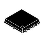
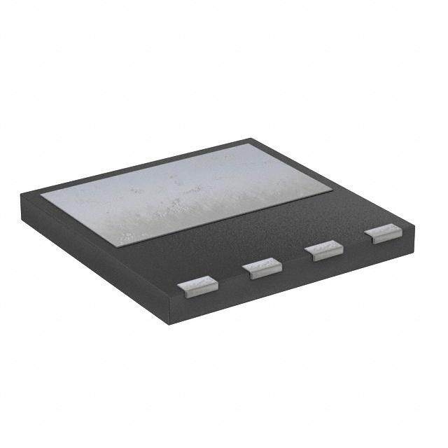
ICGOO电子元器件商城为您提供NTTFS5116PLTAG由ON Semiconductor设计生产,在icgoo商城现货销售,并且可以通过原厂、代理商等渠道进行代购。 NTTFS5116PLTAG价格参考。ON SemiconductorNTTFS5116PLTAG封装/规格:晶体管 - FET,MOSFET - 单, P-Channel 60V 5.7A (Ta) 3.2W (Ta), 40W (Tc) Surface Mount 8-WDFN (3.3x3.3)。您可以下载NTTFS5116PLTAG参考资料、Datasheet数据手册功能说明书,资料中有NTTFS5116PLTAG 详细功能的应用电路图电压和使用方法及教程。
NTTFS5116PLTAG是安森美(ON Semiconductor)推出的一款N沟道功率MOSFET,适用于中低电压开关应用。该器件采用先进的TrenchFET技术,具有低导通电阻(RDS(on))、高效率和优异的热性能,适合在紧凑空间内实现高效功率转换。

其典型应用场景包括:

1. 电源管理:广泛用于DC-DC转换器、同步整流、电压调节模块(VRM)等,提升电源转换效率,降低能耗。
2. 电机驱动:适用于小型直流电机、步进电机的驱动电路,常见于家电、工业控制和电动工具中。
3. 负载开关:用于电池供电设备中的电源通断控制,如笔记本电脑、移动设备和便携式仪器,有效减少待机功耗。
4. 热插拔与电源保护电路:因其快速响应和低损耗特性,可用于防止过流和浪涌电流,保障系统安全。
5. 汽车电子:应用于车载电源系统、车身控制模块(如车窗、座椅驱动)等,满足AEC-Q101车规认证要求,具备良好的可靠性和温度适应性(工作温度可达175°C)。

该MOSFET采用PQFN 5x6封装,体积小、散热好,适合对空间和效率要求较高的设计。综合来看,NTTFS5116PLTAG是一款高性能、高可靠性的功率开关器件,适用于消费电子、工业控制及汽车电子等多种领域。
| 参数 | 数值 |
| 产品目录 | |
| 描述 | MOSFET P-CH 60V 5.7A 8-WDFNMOSFET PFET U8FL 60V |
| 产品分类 | FET - 单分离式半导体 |
| FET功能 | 逻辑电平门 |
| FET类型 | MOSFET P 通道,金属氧化物 |
| Id-ContinuousDrainCurrent | - 20 A |
| Id-连续漏极电流 | - 20 A |
| 品牌 | ON Semiconductor |
| 产品手册 | |
| 产品图片 |
|
| rohs | 符合RoHS无铅 / 符合限制有害物质指令(RoHS)规范要求 |
| 产品系列 | 晶体管,MOSFET,ON Semiconductor NTTFS5116PLTAG- |
| 数据手册 | |
| 产品型号 | NTTFS5116PLTAG |
| Pd-PowerDissipation | 1.6 W, 3.2 W, 20 W, 40 W |
| Pd-功率耗散 | 40 W |
| Qg-GateCharge | 25 nC |
| Qg-栅极电荷 | 25 nC |
| RdsOn-Drain-SourceResistance | 72 mOhms |
| RdsOn-漏源导通电阻 | 72 mOhms |
| Vds-Drain-SourceBreakdownVoltage | - 60 V |
| Vds-漏源极击穿电压 | - 60 V |
| Vgsth-Gate-SourceThresholdVoltage | - 1 V to - 3 V |
| Vgsth-栅源极阈值电压 | - 1 V to - 3 V |
| 不同Id时的Vgs(th)(最大值) | 3V @ 250µA |
| 不同Vds时的输入电容(Ciss) | 1258pF @ 30V |
| 不同Vgs时的栅极电荷(Qg) | 25nC @ 10V |
| 不同 Id、Vgs时的 RdsOn(最大值) | 52 毫欧 @ 6A,10V |
| 产品种类 | MOSFET |
| 供应商器件封装 | 8-WDFN(3.3x3.3) |
| 其它名称 | NTTFS5116PLTAG-ND |
| 功率-最大值 | 3.2W |
| 功率耗散 | 1.6 W, 3.2 W, 20 W, 40 W |
| 包装 | 带卷 (TR) |
| 商标 | ON Semiconductor |
| 安装类型 | 表面贴装 |
| 安装风格 | SMD/SMT |
| 导通电阻 | 72 mOhms |
| 封装 | Reel |
| 封装/外壳 | 8-WDFN 裸露焊盘 |
| 封装/箱体 | WDFN-8 |
| 工厂包装数量 | 1500 |
| 晶体管极性 | P-Channel |
| 最大工作温度 | + 175 C |
| 最小工作温度 | - 55 C |
| 栅极电荷Qg | 25 nC |
| 标准包装 | 1,500 |
| 正向跨导-最小值 | 11 S |
| 汲极/源极击穿电压 | - 60 V |
| 漏极连续电流 | - 20 A |
| 漏源极电压(Vdss) | 60V |
| 电流-连续漏极(Id)(25°C时) | 5.7A (Ta) |
| 系列 | NTTFS5116PL |
| 配置 | Single |


PDF Datasheet 数据手册内容提取
NTTFS5116PL Power MOSFET (cid:2) −60 V, −20 A, 52 m Features • Low R DS(on) • Fast Switching • http://onsemi.com These Devices are Pb−Free and are RoHS Compliant Applications V(BR)DSS RDS(on) MAX ID MAX • Load Switches • 52 m(cid:4) @ −10 V DC Motor Control −60 V −20 A • DC−DC Conversion 72 m(cid:4) @ −4.5 V MAXIMUM RATINGS (TJ = 25°C unless otherwise stated) P−Channel MOSFET Parameter Symbol Value Unit D (5−8) Drain−to−Source Voltage VDSS −60 V Gate−to−Source Voltage VGS ±20 V Continuous Drain TA = 25°C ID −5.7 A Current R(cid:2)JA (Note 1) TA = 100°C −4.0 G (4) Power Dissipation R(cid:2)JA TA = 25°C PD 3.2 W (Note 1) Steady TA = 100°C 1.6 S (1,2,3) Continuous Drain State TC = 25°C ID −20 A Current R(cid:2)JC (Note 1) TC = 100°C −14 MARKING DIAGRAM Power Dissipation TC = 25°C PD 40 W 1 R(cid:2)JC (Note 1) TC = 100°C 20 1 S D WDFN8 S 5116 D Pulsed Drain Current tp = 10 (cid:3)s IDM −76 A ((cid:3)8FL) S AYWW(cid:2) D Operating Junction and Storage Temperature TJ, −55 to °C CASE 511AB G (cid:2) D Tstg +175 Source Current (Body Diode) IS −20 A 5116 = Specific Device Code Single Pulse Drain−to−Source Ava- L = 0.1 mH EAS 45 mJ A = Assembly Location lanche Energy IAS 30 A Y = Year WW = Work Week Lead Temperature for Soldering Purposes TL 260 °C (cid:2) = Pb−Free Package (1/8” from case for 10 s) (Note: Microdot may be in either location) Stresses exceeding Maximum Ratings may damage the device. Maximum Ratings are stress ratings only. Functional operation above the Recommended Operating Conditions is not implied. Extended exposure to stresses above the Recommended Operating Conditions may affect device reliability. ORDERING INFORMATION Device Package Shipping† THERMAL RESISTANCE MAXIMUM RATINGS NTTFS5116PLTAG WDFN8 1500/Tape & Reel Parameter Symbol Value Unit (Pb−Free) Junction−to−Case – Steady R(cid:2)JC 3.8 °C/W NTTFS5116PLTWG WDFN8 5000/Tape & Reel State (Note 1) (Pb−Free) Junction−to−Ambient – Steady R(cid:2)JA 47 †For information on tape and reel specifications, State (Note 1) including part orientation and tape sizes, please 1. Surface−mounted on FR4 board using 1 in sq pad size (Cu area = 1.127 in sq refer to our Tape and Reel Packaging Specification [2 oz] including traces. Brochure, BRD8011/D. © Semiconductor Components Industries, LLC, 2011 1 Publication Order Number: November, 2011 − Rev. 1 NTTFS5116PL/D
NTTFS5116PL ELECTRICAL CHARACTERISTICS (TJ = 25°C unless otherwise specified) Parameter Symbol Test Condition Min Typ Max Unit OFF CHARACTERISTICS Drain−to−Source Breakdown Voltage V(BR)DSS VGS = 0 V, ID = −250 (cid:3)A −60 V Drain−to−Source Breakdown Voltage V(BR)DSS/TJ 69.7 mV/°C Temperature Coefficient Zero Gate Voltage Drain Current IDSS VGS = 0 V, TJ = 25°C −1.0 (cid:3)A VDS = −60 V TJ = 125°C −100 Gate−to−Source Leakage Current IGSS VDS = 0 V, VGS = ±20 V ±100 nA ON CHARACTERISTICS (Note 2) Gate Threshold Voltage VGS(TH) VGS = VDS, ID = −250 (cid:3)A −1 −3 V Negative Threshold Temperature VGS(TH)/TJ −6.2 mV/°C Coefficient Drain−to−Source On Resistance RDS(on) VGS = −10 V ID = −6 A 37 52 m(cid:4) VGS = −4.5 V ID = −4.4 A 51 72 Forward Transconductance gFS VDS = −15 V, ID = −6 A 11 S CHARGES, CAPACITANCES AND GATE RESISTANCE Input Capacitance Ciss 1258 pF Output Capacitance Coss VGS = 0 V, f = 1.0 MHz, VDS = −30 V 127 Reverse Transfer Capacitance Crss 84 Total Gate Charge QG(TOT) VGS = −10 V, VDS = −48 V, ID = −5 A 25 nC VGS = −4.5 V, VDS = −48 V, ID = −5 A 14 Threshold Gate Charge QG(TH) 1 nC Gate−to−Source Charge QGS 4 VGS = −4.5 V, VDS = −48 V, ID = −5 A Gate−to−Drain Charge QGD 7 Plateau Voltage VGP 3.1 V Gate Resistance RG 5.3 (cid:4) SWITCHING CHARACTERISTICS (Note 3) Turn−On Delay Time td(on) 15 ns Rise Time tr VGS = −4.5 V, VDS = −48 V, 58 Turn−Off Delay Time td(off) ID = −5 A, RG = 6 (cid:4) 30 Fall Time tf 37 DRAIN−SOURCE DIODE CHARACTERISTICS Forward Diode Voltage VSD VGS = 0 V, TJ = 25°C −0.79 −1.2 V IS = −5 A TJ = 125°C −0.64 Reverse Recovery Time tRR 20 ns Charge Time ta VGS = 0 V, dIS/dt = −100 A/(cid:3)s, 15 Discharge Time tb IS = −5 A 5 Reverse Recovery Charge QRR 19 nC 2. Pulse Test: pulse width (cid:2) 300 (cid:3)s, duty cycle (cid:2) 2%. 3. Switching characteristics are independent of operating junction temperatures. http://onsemi.com 2
NTTFS5116PL TYPICAL CHARACTERISTICS 40 40 VDS ≥ 10 V VGS = 10 V VGS = 4.5 V T (A) 30 T (A) 30 N N E E R R R VGS = 4 V R U 20 U 20 C C N N AI AI , DRD 10 VGS = 3.5 V , DRD 10 TJ = 25°C I I VGS = 3 V TJ = 125°C TJ = −55°C 0 0 0 1 2 3 4 5 2 3 4 5 6 VDS, DRAIN−TO−SOURCE VOLTAGE (V) VGS, GATE−TO−SOURCE VOLTAGE (V) Figure 1. On−Region Characteristics Figure 2. Transfer Characteristics (cid:4)) (cid:4)) E ( 0.075 E ( 0.080 C C AN ID = −6 A AN TJ = 25°C ST TJ = 25°C ST 0.070 SI 0.065 SI E E R R E E C C 0.060 UR 0.055 UR VGS = 4.5 V O O S S − − 0.050 O O T T − − N 0.045 N RAI RAI 0.040 VGS = 10 V D D , n) , n) S(o0.035 S(o0.030 D 2 4 6 8 10D 5 10 15 20 25 30 35 40 R R VGS, GATE−TO−SOURCE VOLTAGE (V) ID, DRAIN CURRENT (A) Figure 3. On−Resistance vs. Gate−to−Source Figure 4. On−Resistance vs. Drain Current and Voltage Gate Voltage 2.0 10,000 S- ID = −4.4 A VGS = 0 V RE 1.8 VGS = 4.5 V E D) RCZE1.6 A) OUALI E (n TJ = 150°C SM1.4 G DRAIN−TO−ANCE (NOR11..02 , LEAKADSS1,000 TJ = 125°C , n)ST I S(oI0.8 D R 0.6 100 −50 −25 0 25 50 75 100 125 150 175 10 20 30 40 50 60 TJ, JUNCTION TEMPERATURE (°C) −VDS, DRAIN−TO−SOURCE VOLTAGE (V) Figure 5. On−Resistance Variation with Figure 6. Drain−to−Source Leakage Current Temperature vs. Voltage http://onsemi.com 3
NTTFS5116PL TYPICAL CHARACTERISTICS 1800 10 1600 VGS = 0 V GE QT pF)1400 Ciss TJ = 25°C VOLTA 8 E (1200 CE C R 6 N1000 U TA OV) CI 800 −S( APA 600 −TO 4 Qgs Qgd C E C, 400 GAT 2 VDS = −48 V 2000 Crss Coss V, GS 0 ITDJ == −255 °AC 0 10 20 30 40 50 60 0 5 10 15 20 25 VDS, DRAIN−TO−SOURCE VOLTAGE (V) Qg, TOTAL GATE CHARGE (nC) Figure 7. Capacitance Variation Figure 8. Gate−to−Source and Drain−to−Source Voltage vs. Total Charge 1000 40 VDD = −48 V VGS = 0 V ID = −5 A A) TJ = 25°C VGS = −4.5 V T ( 30 N 100 E s) tf RR E (n tr CU 20 M E t, TI 10 td(on) td(off) OURC S 10 , S −I 1 0 1 10 100 0.5 0.6 0.7 0.8 0.9 1.0 1.1 RG, GATE RESISTANCE ((cid:4)) −VSD, SOURCE−TO−DRAIN VOLTAGE (V) Figure 9. Resistive Switching Time Variation Figure 10. Diode Forward Voltage vs. Current vs. Gate Resistance 100 45 T (A) VSTCiGn Sg= l =e2 5−P°1uC0ls Ve 10 ms1 ms 10100 (cid:3) (cid:3)ss AIN−TO−ERGY (mJ) N 10 RN 30 E dc DE RR E E U SH N C PULANC AI E L −I, DRD 1 RThDeSr(mona) lL Limimitit , SINGLSRCE AVA 15 AU Package Limit EO S 0.1 0 0.1 1 10 100 25 50 75 100 125 150 175 −VDS, DRAIN−TO−SOURCE VOLTAGE (V) TJ, STARTING JUNCTION TEMPERATURE (°C) Figure 11. Maximum Rated Forward Biased Figure 12. Maximum Avalanche Energy vs. Safe Operating Area Starting Junction Temperature http://onsemi.com 4
NTTFS5116PL TYPICAL CHARACTERISTICS 100 D = 0.5 10 D = 0.2 D = 0.1 D = 0.05 (t)A 1 D = 0.02 (cid:2)J D = 0.01 R 0.1 Single Pulse 0.01 0.000001 0.00001 0.0001 0.001 0.01 0.1 1 10 100 1000 PULSE TIME (sec) Figure 13. Thermal Response http://onsemi.com 5
NTTFS5116PL PACKAGE DIMENSIONS WDFN8 3.3x3.3, 0.65P CASE 511AB ISSUE C 2X 0.20 C NOTES: 1. DIMENSIONING AND TOLERANCING PER ASME Y14.5M, 1994. 2. CONTROLLING DIMENSION: MILLIMETERS. D A 3. DIMENSION D1 AND E1 DO NOT INCLUDE MOLD FLASH B PROTRUSIONS OR GATE BURRS. D1 2X 0.20 C MILLIMETERS INCHES 8 7 6 5 DIM MIN NOM MAX MIN NOM MAX A 0.70 0.75 0.80 0.028 0.030 0.031 4X A1 0.00 (cid:3)(cid:3)(cid:3) 0.05 0.000 (cid:3)(cid:3)(cid:3) 0.002 E1 E (cid:4) b 0.23 0.30 0.40 0.009 0.012 0.016 c 0.15 0.20 0.25 0.006 0.008 0.010 D 3.30 BSC 0.130 BSC 1 2 3 4 c A1 DD12 12..9985 32..0115 32..1254 00..011768 00..102803 00..102848 TOP VIEW E 3.30 BSC 0.130 BSC E1 2.95 3.05 3.15 0.116 0.120 0.124 0.10 C E2 1.47 1.60 1.73 0.058 0.063 0.068 E3 0.23 0.30 0.40 0.009 0.012 0.016 A C e 0.65 BSC 0.026 BSC 0.10 C 6eX SPELAATNINEG GK 00..3604 (cid:3)0.(cid:3)41(cid:3) (cid:3)0.(cid:3)51(cid:3) 00..001225 0(cid:3).0(cid:3)16(cid:3) 0(cid:3).0(cid:3)20(cid:3) L 0.30 0.43 0.56 0.012 0.017 0.022 SIDE VIEW DETAIL A DETAIL A L1 0.06 0.13 0.20 0.002 0.005 0.008 M 1.40 1.50 1.60 0.055 0.059 0.063 (cid:4) 0° (cid:3)(cid:3)(cid:3) 12° 0° (cid:3)(cid:3)(cid:3) 12° 8X 0.10(cid:2)(cid:2)C(cid:2)A (cid:4)(cid:5)B SOLDERING FOOTPRINT* 0.05 C 8X 4XL e/2 0.42 0.65 4X 14 PITCH 0.66 PACKAGE K OUTLINE E2 E3 M 8 5 L1 3.60 G D2 BOTTOM VIEW 0.75 0.57 2.30 0.47 2.37 3.46 DIMENSION: MILLIMETERS *For additional information on our Pb(cid:3)Free strategy and soldering details, please download the ON Semiconductor Soldering and Mounting Techniques Reference Manual, SOLDERRM/D. ON Semiconductor and are registered trademarks of Semiconductor Components Industries, LLC (SCILLC). SCILLC reserves the right to make changes without further notice to any products herein. SCILLC makes no warranty, representation or guarantee regarding the suitability of its products for any particular purpose, nor does SCILLC assume any liability arising out of the application or use of any product or circuit, and specifically disclaims any and all liability, including without limitation special, consequential or incidental damages. “Typical” parameters which may be provided in SCILLC data sheets and/or specifications can and do vary in different applications and actual performance may vary over time. All operating parameters, including “Typicals” must be validated for each customer application by customer’s technical experts. SCILLC does not convey any license under its patent rights nor the rights of others. SCILLC products are not designed, intended, or authorized for use as components in systems intended for surgical implant into the body, or other applications intended to support or sustain life, or for any other application in which the failure of the SCILLC product could create a situation where personal injury or death may occur. Should Buyer purchase or use SCILLC products for any such unintended or unauthorized application, Buyer shall indemnify and hold SCILLC and its officers, employees, subsidiaries, affiliates, and distributors harmless against all claims, costs, damages, and expenses, and reasonable attorney fees arising out of, directly or indirectly, any claim of personal injury or death associated with such unintended or unauthorized use, even if such claim alleges that SCILLC was negligent regarding the design or manufacture of the part. SCILLC is an Equal Opportunity/Affirmative Action Employer. This literature is subject to all applicable copyright laws and is not for resale in any manner. PUBLICATION ORDERING INFORMATION LITERATURE FULFILLMENT: N. American Technical Support: 800−282−9855 Toll Free ON Semiconductor Website: www.onsemi.com Literature Distribution Center for ON Semiconductor USA/Canada P.O. Box 5163, Denver, Colorado 80217 USA Europe, Middle East and Africa Technical Support: Order Literature: http://www.onsemi.com/orderlit Phone: 303−675−2175 or 800−344−3860 Toll Free USA/Canada Phone: 421 33 790 2910 Fax: 303−675−2176 or 800−344−3867 Toll Free USA/Canada Japan Customer Focus Center For additional information, please contact your local Email: orderlit@onsemi.com Phone: 81−3−5817−1050 Sales Representative http://onsemi.com NTTFS5116PL/D 6
Mouser Electronics Authorized Distributor Click to View Pricing, Inventory, Delivery & Lifecycle Information: O N Semiconductor: NTTFS5116PLTAG NTTFS5116PLTWG