ICGOO在线商城 > 分立半导体产品 > 晶体管 - FET,MOSFET - 单 > FDD8444

 Datasheet下载
- 型号: FDD8444
- 制造商: Fairchild Semiconductor
- 库位|库存: xxxx|xxxx
- 要求:
| 数量阶梯 | 香港交货 | 国内含税 |
| +xxxx | $xxxx | ¥xxxx |
查看当月历史价格
查看今年历史价格
FDD8444产品简介:
ICGOO电子元器件商城为您提供FDD8444由Fairchild Semiconductor设计生产,在icgoo商城现货销售,并且可以通过原厂、代理商等渠道进行代购。 FDD8444价格参考。Fairchild SemiconductorFDD8444封装/规格:晶体管 - FET,MOSFET - 单, 表面贴装 N 沟道 40V 145A(Tc) 153W(Tc) TO-252AA。您可以下载FDD8444参考资料、Datasheet数据手册功能说明书,资料中有FDD8444 详细功能的应用电路图电压和使用方法及教程。
FDD8444 是由 ON Semiconductor(安森美半导体)生产的一款 N 沟道增强型 MOSFET,属于晶体管 - FET、MOSFET - 单类别。该型号具有低导通电阻(Rds(on))、高开关速度和良好的热性能,适用于多种电力电子应用场景。以下是其主要应用场景:

1. 直流电机驱动
   FDD8444 的低导通电阻特性使其非常适合用于小型直流电机的驱动电路中,能够高效地控制电机的启停、转向和速度调节。

2. 开关电源 (SMPS)
   在开关电源设计中,FDD8444 可作为功率开关使用,适用于降压(Buck)、升压(Boost)或反激式(Flyback)转换器,提供高效的电压转换。

3. 负载开关
   由于其低导通电阻和快速开关能力,FDD8444 能够在负载开关应用中实现低损耗的电流传输,同时支持快速开启和关闭功能。

4. 电池管理
   在便携式设备(如智能手机、平板电脑等)的电池管理系统中,FDD8444 可用于电池充放电路径的控制,确保电流流向的安全性和效率。

5. LED 驱动
   该 MOSFET 可用于 LED 照明驱动电路中,通过 PWM(脉宽调制)控制 LED 的亮度,同时保持较低的功耗。

6. 汽车电子
   FDD8444 可应用于汽车电子中的简单负载控制,例如车窗升降器、座椅调节器或其他低功率车载设备。

7. 信号切换
   在需要高频信号切换的应用中,FDD8444 的低栅极电荷和快速开关特性使其成为理想选择,适用于音频信号切换或数据通信线路的控制。

总结来说,FDD8444 凭借其优异的电气特性和可靠性,广泛应用于消费电子、工业控制、汽车电子和通信设备等领域,特别是在需要高效功率转换和低损耗的场景中表现出色。
| 参数 | 数值 |
| 产品目录 | |
| ChannelMode | Enhancement |
| 描述 | MOSFET N-CH 40V 145A DPAKMOSFET LOW VOLTAGE |
| 产品分类 | FET - 单分离式半导体 |
| FET功能 | 标准 |
| FET类型 | MOSFET N 通道,金属氧化物 |
| Id-ContinuousDrainCurrent | 145 A |
| Id-连续漏极电流 | 145 A |
| 品牌 | Fairchild Semiconductor |
| 产品手册 | |
| 产品图片 |
|
| rohs | RoHS 合规性豁免无铅 / 符合限制有害物质指令(RoHS)规范要求 |
| 产品系列 | 晶体管,MOSFET,Fairchild Semiconductor FDD8444PowerTrench® |
| 数据手册 | |
| 产品型号 | FDD8444 |
| PCN封装 | |
| Pd-PowerDissipation | 153 W |
| Pd-功率耗散 | 153 W |
| RdsOn-Drain-SourceResistance | 5.2 mOhms |
| RdsOn-漏源导通电阻 | 5.2 mOhms |
| Vds-Drain-SourceBreakdownVoltage | 40 V |
| Vds-漏源极击穿电压 | 40 V |
| Vgs-Gate-SourceBreakdownVoltage | +/- 20 V |
| Vgs-栅源极击穿电压 | 20 V |
| 上升时间 | 78 ns |
| 下降时间 | 15 ns |
| 不同Id时的Vgs(th)(最大值) | 4V @ 250µA |
| 不同Vds时的输入电容(Ciss) | 6195pF @ 25V |
| 不同Vgs时的栅极电荷(Qg) | 116nC @ 10V |
| 不同 Id、Vgs时的 RdsOn(最大值) | 5.2 毫欧 @ 50A,10V |
| 产品目录页面 | |
| 产品种类 | MOSFET |
| 供应商器件封装 | D-Pak |
| 其它名称 | FDD8444CT |
| 典型关闭延迟时间 | 48 ns |
| 功率-最大值 | 153W |
| 包装 | 剪切带 (CT) |
| 单位重量 | 260.370 mg |
| 商标 | Fairchild Semiconductor |
| 安装类型 | 表面贴装 |
| 安装风格 | SMD/SMT |
| 封装 | Reel |
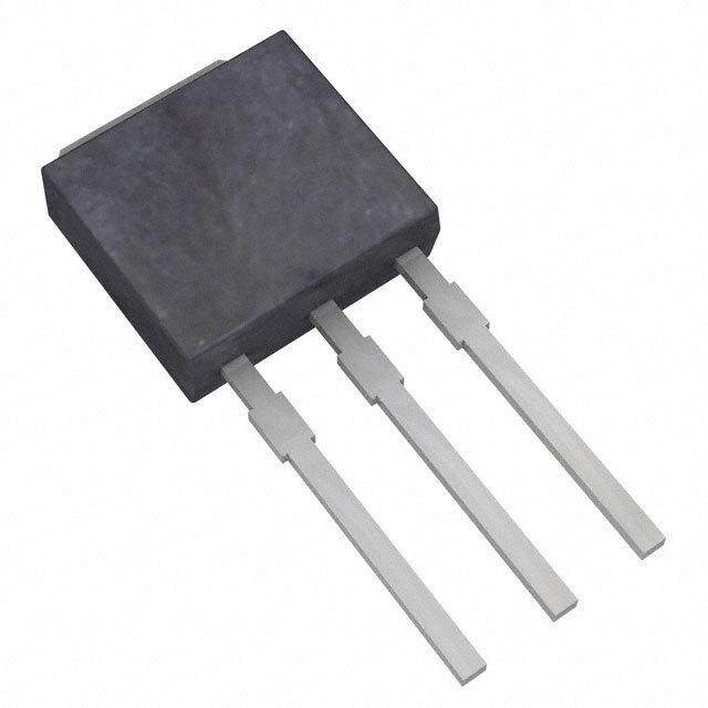
| 封装/外壳 | TO-252-3,DPak(2 引线+接片),SC-63 |
| 封装/箱体 | DPAK-2 |
| 工厂包装数量 | 2500 |
| 晶体管极性 | N-Channel |
| 最大工作温度 | + 175 C |
| 最小工作温度 | - 55 C |
| 标准包装 | 1 |
| 漏源极电压(Vdss) | 40V |
| 电流-连续漏极(Id)(25°C时) | 145A (Tc) |
| 系列 | FDD8444 |
| 通道模式 | Enhancement |
| 配置 | Single |


PDF Datasheet 数据手册内容提取
Is Now Part of To learn more about ON Semiconductor, please visit our website at www.onsemi.com Please note: As part of the Fairchild Semiconductor integration, some of the Fairchild orderable part numbers will need to change in order to meet ON Semiconductor’s system requirements. Since the ON Semiconductor product management systems do not have the ability to manage part nomenclature that utilizes an underscore (_), the underscore (_) in the Fairchild part numbers will be changed to a dash (-). This document may contain device numbers with an underscore (_). Please check the ON Semiconductor website to verify the updated device numbers. The most current and up-to-date ordering information can be found at www.onsemi.com. Please email any questions regarding the system integration to Fairchild_questions@onsemi.com. ON Semiconductor and the ON Semiconductor logo are trademarks of Semiconductor Components Industries, LLC dba ON Semiconductor or its subsidiaries in the United States and/or other countries. ON Semiconductor owns the rights to a number of patents, trademarks, copyrights, trade secrets, and other intellectual property. A listing of ON Semiconductor’s product/patent coverage may be accessed at www.onsemi.com/site/pdf/Patent-Marking.pdf. ON Semiconductor reserves the right to make changes without further notice to any products herein. ON Semiconductor makes no warranty, representation or guarantee regarding the suitability of its products for any particular purpose, nor does ON Semiconductor assume any liability arising out of the application or use of any product or circuit, and specifically disclaims any and all liability, including without limitation special, consequential or incidental damages. Buyer is responsible for its products and applications using ON Semiconductor products, including compliance with all laws, regulations and safety requirements or standards, regardless of any support or applications information provided by ON Semiconductor. “Typical” parameters which may be provided in ON Semiconductor data sheets and/or specifications can and do vary in different applications and actual performance may vary over time. All operating parameters, including “Typicals” must be validated for each customer application by customer’s technical experts. ON Semiconductor does not convey any license under its patent rights nor the rights of others. ON Semiconductor products are not designed, intended, or authorized for use as a critical component in life support systems or any FDA Class 3 medical devices or medical devices with a same or similar classification in a foreign jurisdiction or any devices intended for implantation in the human body. Should Buyer purchase or use ON Semiconductor products for any such unintended or unauthorized application, Buyer shall indemnify and hold ON Semiconductor and its officers, employees, subsidiaries, affiliates, and distributors harmless against all claims, costs, damages, and expenses, and reasonable attorney fees arising out of, directly or indirectly, any claim of personal injury or death associated with such unintended or unauthorized use, even if such claim alleges that ON Semiconductor was negligent regarding the design or manufacture of the part. ON Semiconductor is an Equal Opportunity/Affirmative Action Employer. This literature is subject to all applicable copyright laws and is not for resale in any manner.
F D D 8 4 March 2015 4 4 FDD8444 N - C ® h N-Channel PowerTrench MOSFET a n n 40V, 50A, 5.2mΩ e l P Features Applications o w (cid:132) Typ rDS(on) = 4mΩ at VGS = 10V, ID = 50A (cid:132) Automotive Engine Control er T (cid:132) Typ Qg(10) = 89nC at VGS = 10V (cid:132) Powertrain Management r e (cid:132) Low Miller Charge (cid:132) Solenoid and Motor Drivers n c h (cid:132) Low Qrr Body Diode (cid:132) Electronic Transmission ® (cid:132) UIS Capability (Single Pulse/ Repetitive Pulse) (cid:132) Distributed Power Architecture and VRMs M O (cid:132) Qualified to AEC Q101 (cid:132) Primary Switch for 12V Systems S F (cid:132) RoHS Compliant E T LEA D FREEIMPL EM E N T A NOIT ©2006 Fairchild Semiconductor Corporation 1 www.fairchildsemi.com FDD8444 Rev. 1.(cid:21)
F MOSFET Maximum Ratings TC = 25°C unless otherwise noted D D Symbol Parameter Ratings Units 8 4 V Drain to Source Voltage 40 V 4 DSS 4 V Gate to Source Voltage ±20 V GS N Drain Current Continuous (V = 10V) (Note 1) 145 - GS C ID Continuous (VGS = 10V, with RθJA = 52oC/W) 20 A h a Pulsed Figure 4 n E Single Pulse Avalanche Energy (Note 2) 535 mJ n AS e Power Dissipation 153 W l PD Derate above 25oC 1.02 W/oC Po T , T Operating and Storage Temperature -55 to +175 oC w J STG e Thermal Characteristics r T r e R Thermal Resistance, Junction to Case 0.98 oC/W n θJC c R Thermal Resistance, Junction to Ambient TO-252, 1in2 copper pad area 52 oC/W h θJA ® M Package Marking and Ordering Information O S Device Marking Device Package Reel Size Tape Width Quantity F E FDD8444 FDD8444 TO-252AA 13” 16mm 2500 units T Electrical Characteristics T = 25°C unless otherwise noted J Symbol Parameter Test Conditions Min Typ Max Units Off Characteristics B Drain to Source Breakdown Voltage I = 250μA, V = 0V 40 - - V VDSS D GS V = 32V - - 1 I Zero Gate Voltage Drain Current DS μA DSS V = 0V T = 150oC - - 250 GS J I Gate to Source Leakage Current V = ±20V - - ±100 nA GSS GS On Characteristics V Gate to Source Threshold Voltage V = V , I = 250μA 2 2.5 4 V GS(th) GS DS D I = 50A, V = 10V - 4 5.2 D GS rDS(on) Drain to Source On Resistance ID = 50A, VGS= 10V, - 7.2 9.4 mΩ T = 175oC J Dynamic Characteristics C Input Capacitance - 6195 - pF iss V = 25V, V = 0V, C Output Capacitance DS GS - 585 - pF oss f = 1MHz C Reverse Transfer Capacitance - 332 - pF rss R Gate Resistance f = 1MHz - 1.9 - Ω G Q Total Gate Charge at 10V V = 0 to 10V - 89 116 nC g(TOT) GS Q Total Gate Charge at 5V V = 0 to 5V 43 56 nC g(5) GS V = 20V Q Threshold Gate Charge V = 0 to 2V DD - 11 14.3 nC g(TH) GS I = 50A Q Gate to Source Gate Charge D - 23 - nC gs Ig = 1.0mA Q Gate Charge Threshold to Plateau - 11 - nC gs2 Q Gate to Drain “Miller“ Charge - 20 - nC gd FDD8444 Rev. 1.(cid:21) 2 www.fairchildsemi.com
F Electrical Characteristics T = 25oC unless otherwise noted D J D 8 Symbol Parameter Test Conditions Min Typ Max Units 4 4 Switching Characteristics 4 N - t Turn-On Time - - 135 ns C on h t Turn-On Delay Time - 12 - ns d(on) a t Turn-On Rise Time VDD = 20V, ID = 50A - 78 - ns n r V = 10V, R = 2Ω n td(off) Turn-Off Delay Time GS GS - 48 - ns e l tf Turn-Off Fall Time - 15 - ns P t Turn-Off Time - - 95 ns o off w e Drain-Source Diode Characteristics r T r VSD Source to Drain Diode Voltage IISD == 5205AA -- 00..98 11.2.05 V en SD c t Reverse Recovery Time - 39 51 ns h rr I = 50A, dI /dt = 100A/μs ® Qrr Reverse Recovery Charge F F - 45 59 nC M O Notes: S 1: Package current limitation is 50A. 2: Starting TJ = 25oC, L = 0.67mH, IAS = 40A FE T This product has been designed to meet the extreme test conditions and environment demanded by the automotive industry. For a copy of the requirements, see AEC Q101 at: http://www.aecouncil.com/ All Fairchild Semiconductor products are manufactured, assembled and tested under ISO9000 and QS9000 quality systems certification. FDD8444 Rev. 1.(cid:21) 3 www.fairchildsemi.com
F D Typical Characteristics D 8 4 4 4 1.2 160 MULIPLIER01..80 NT (A)112400 BCYU RPRAECNKTA LGIEMITED VGS = 10V N-Chan N E100 n DISSIPATIO00..46 RAIN CURR 6800 el Pow WER 0.2 I, DD 2400 erT O r P e 0.0 0 n 0 25 50 75 100 125 150 175 25 50 75 100 125 150 175 c h TC, CASE TEMPERATURE(oC) TC, CASE TEM PERATURE(oC) ® M Figure 1. Normalized Power Dissipation vs Case Figure 2. Maximum Continuous Drain Current vs O Temperature Case Temperature S F 2 E DUTY CYCLE - DESCENDING ORDER T 1 L A M C D THERNCE, ZJθ D = 0000....21050050 PDM ALIZEPEDA0.1 00..0021 t1t2 MM NOTES: ORI DUTY FACTOR: D = t1/t2 N PEAK TJ = PDM x ZθJC x RθJC + TC SINGLE PULSE 0.01 10-5 10-4 10-3 10-2 10-1 100 101 t, RECTANGULAR PULSE DURATION(s) Figure 3. Normalized Maximum Transient Thermal Impedance 2000 VGS = 10V TRANSCONDUCTANCE TC = 25oC 1000 MAY LIMIT CURRENT FOR TEMPERATURES T (A) IN THIS REGION CABU ORRVEEN 2T5 oACS D FEORLALTOEW PSE:AK EN I = I25 175 - TC R 150 R U C K 100 A E P , M D I SINGLE PULSE 10 10-5 10-4 10-3 10-2 10-1 100 101 t, RECTANGULAR PULSE DURATION(s) Figure 4. Peak Current Capability FDD8444 Rev. 1.(cid:21) 4 www.fairchildsemi.com
F Typical Characteristics D D 8 4 1000 500 4 If R = 0 4 T (A)100 10us NT (A)100 tItfAA RVV ==≠ ((0LL)/R(IA)lSn)[/((I1A.S3**RR)A/(T1E.3D*R BAVTDESDS -B VVDDDS)S - VDD) +1] N-C REN 100us URRE ha RN CU 10 CHE C STARTING TJ = 25oC nne , DRAID 1 CBUY RPRAECNKTA GLIEMITED 1ms LANAVA 10 STARTING TJ = 150oC l Pow I 0.11ALOIRPMEEITARE AMDTA IBOYYN B rIEDN S T(oHnIS) STTJCIN ==G M2L5EAo1 XCP0 URLASTEED 10DmCs 100 I, AS 01.01 0.1 1 10 100 1000 erTren VDS, DRAIN TO SOURCE VOLTAGE (V) tAV, TIME IN AVALANCHE (ms) c h NOTE: Refer to Fairchild Application Notes AN7514 and AN7515 ® Figure 5. Forward Bias Safe Operating Area Figure 6. Unclamped Inductive Switching M Capability O S F E 100 100 T PULSE DURATION = 80μs VGS = 10V PULSE DURATION = 80μs DUTY CYCLE = 0.5% MAX DUTY CYCLE = 0.5% MAX IN CURRENT (A)I, DRAD 24680000 VDD = 5V TJT =J =25 1o7C5oC TJ = -55oC I, DRAIN CURRENT (A)D24680000 VGS = 5V VVGSG S= =4 .45VV 0 0 2.0 2.5 3.0 3.5 4.0 4.5 5.0 0.0 0.3 0.6 0.9 1.2 1.5 VGS, GATE TO SOURCE VOLTAGE (V) VDS, DRAIN TO SOURCE VOLTAGE (V) Figure 7. Transfer Characteristics Figure 8. Saturation Characteristics 14 E1.8 ID = 50A DPUULTSYE C DYUCRLEA T=I O0.N5 %= 8M0AμXs NC PULSE DURATION = 80μs RCE )Ω12 SISTA1.6 DUTY CYCLE = 0.5% MAX N TO SOUmTANCE (108 TJ = 175oC MALIZEDCE ON-RE11..24 r, DRAIDS(on)ON-RESIS 46 TJ = 25oC NORAIN TO SOUR01..80 VIDG S= =5 01A0V 2 DR0.6 4 5 6 7 8 9 10 -80 -40 0 40 80 120 160 200 VGS, GATE TO SOURCE VOLTAGE (V) TJ, JUNCTION TEMPERATURE(oC) Figure 9. Drain to Source On-Resistance Figure 10. Normalized Drain to Source On Variation vs Gate to Source Voltage Resistance vs Junction Temperature FDD8444 Rev. 1.(cid:21) 5 www.fairchildsemi.com
F Typical Characteristics D D 8 4 4 1.2 1.15 4 1.1 VGS = VDS CE ID = 250μA N E ID = 250μA URE 1.10 -C TE AG1.0 SOAG h ZED GAD VOLT00..89 AIN TO N VOLT1.05 anne ALINORMTHRESHOL00..67 ALIZED DRREAKDOW01..9050 l Powe 0.5 RMB rT O r 0.4 N 0.90 e -80 -40 0 40 80 120 160 200 -80 -40 0 40 80 120 160 200 n TJ, JUNCTION TEMPERATURE(oC) TJ, JUNCTION TEMPERATURE (oC) ch ® Figure 11. Normalized Gate Threshold Voltage vs Figure 12. Normalized Drain to Source M Junction Temperature Breakdown Voltage vs Junction Temperature O S F E 10000 E(V)10 ID = 50A T G A pF) Ciss OLT 8 VDD = 15V CITANCE (PA1000 Coss O SOURCE V 46 VDD = 20V VDD = 25V A T C Crss TE A 2 f = 1MHz G VGS = 0V , GS 100 V 0 0.1 1 10 40 0 20 40 60 80 100 VDS, DRAIN TO SOURCE VOLTAGE (V) Qg, GATE CHARGE(nC) Figure 13. Capacitance vs Drain to Source Figure 14. Gate Charge vs Gate to Source Voltage Voltage FDD8444 Rev. 1.(cid:21) 6 www.fairchildsemi.com
None
ON Semiconductor and are trademarks of Semiconductor Components Industries, LLC dba ON Semiconductor or its subsidiaries in the United States and/or other countries. ON Semiconductor owns the rights to a number of patents, trademarks, copyrights, trade secrets, and other intellectual property. A listing of ON Semiconductor’s product/patent coverage may be accessed at www.onsemi.com/site/pdf/Patent−Marking.pdf. ON Semiconductor reserves the right to make changes without further notice to any products herein. ON Semiconductor makes no warranty, representation or guarantee regarding the suitability of its products for any particular purpose, nor does ON Semiconductor assume any liability arising out of the application or use of any product or circuit, and specifically disclaims any and all liability, including without limitation special, consequential or incidental damages. Buyer is responsible for its products and applications using ON Semiconductor products, including compliance with all laws, regulations and safety requirements or standards, regardless of any support or applications information provided by ON Semiconductor. “Typical” parameters which may be provided in ON Semiconductor data sheets and/or specifications can and do vary in different applications and actual performance may vary over time. All operating parameters, including “Typicals” must be validated for each customer application by customer’s technical experts. ON Semiconductor does not convey any license under its patent rights nor the rights of others. ON Semiconductor products are not designed, intended, or authorized for use as a critical component in life support systems or any FDA Class 3 medical devices or medical devices with a same or similar classification in a foreign jurisdiction or any devices intended for implantation in the human body. Should Buyer purchase or use ON Semiconductor products for any such unintended or unauthorized application, Buyer shall indemnify and hold ON Semiconductor and its officers, employees, subsidiaries, affiliates, and distributors harmless against all claims, costs, damages, and expenses, and reasonable attorney fees arising out of, directly or indirectly, any claim of personal injury or death associated with such unintended or unauthorized use, even if such claim alleges that ON Semiconductor was negligent regarding the design or manufacture of the part. ON Semiconductor is an Equal Opportunity/Affirmative Action Employer. This literature is subject to all applicable copyright laws and is not for resale in any manner. PUBLICATION ORDERING INFORMATION LITERATURE FULFILLMENT: N. American Technical Support: 800−282−9855 Toll Free ON Semiconductor Website: www.onsemi.com Literature Distribution Center for ON Semiconductor USA/Canada 19521 E. 32nd Pkwy, Aurora, Colorado 80011 USA Europe, Middle East and Africa Technical Support: Order Literature: http://www.onsemi.com/orderlit Phone: 303−675−2175 or 800−344−3860 Toll Free USA/Canada Phone: 421 33 790 2910 Fax: 303−675−2176 or 800−344−3867 Toll Free USA/Canada Japan Customer Focus Center For additional information, please contact your local Email: orderlit@onsemi.com Phone: 81−3−5817−1050 Sales Representative © Semiconductor Components Industries, LLC www.onsemi.com www.onsemi.com 1
Mouser Electronics Authorized Distributor Click to View Pricing, Inventory, Delivery & Lifecycle Information: O N Semiconductor: FDD8444