ICGOO在线商城 > 分立半导体产品 > 晶体管 - FET,MOSFET - 单 > FDMC86106LZ

 Datasheet下载
- 型号: FDMC86106LZ
- 制造商: Fairchild Semiconductor
- 库位|库存: xxxx|xxxx
- 要求:
| 数量阶梯 | 香港交货 | 国内含税 |
| +xxxx | $xxxx | ¥xxxx |
查看当月历史价格
查看今年历史价格
FDMC86106LZ产品简介:
ICGOO电子元器件商城为您提供FDMC86106LZ由Fairchild Semiconductor设计生产,在icgoo商城现货销售,并且可以通过原厂、代理商等渠道进行代购。 FDMC86106LZ价格参考。Fairchild SemiconductorFDMC86106LZ封装/规格:晶体管 - FET,MOSFET - 单, 表面贴装 N 沟道 100V 3.3A(Ta),7.5A(Tc) 2.3W(Ta),19W(Tc) 8-MLP(3.3x3.3)。您可以下载FDMC86106LZ参考资料、Datasheet数据手册功能说明书,资料中有FDMC86106LZ 详细功能的应用电路图电压和使用方法及教程。
FDMC86106LZ 是由 ON Semiconductor(安森美半导体)生产的一款 N 沟道增强型 MOSFET,属于晶体管 - FET、MOSFET - 单类别的产品。该型号的主要应用场景包括:

1. 电源管理:
   FDMC86106LZ 适用于各种开关电源(SMPS)设计,例如 DC-DC 转换器、降压/升压转换器等。其低导通电阻(Rds(on))特性能够减少功率损耗,提高效率,特别适合需要高效能的电源管理系统。

2. 电机驱动:
   该 MOSFET 可用于小型直流电机或步进电机的驱动电路中,提供高效的开关控制。其快速开关能力和较低的功耗使其成为电机驱动应用的理想选择。

3. 负载切换:
   在消费电子、工业设备和汽车电子中,FDMC86106LZ 可用作负载切换开关,实现对不同负载的有效控制,例如 LED 照明、传感器模块或其他外围设备。

4. 电池保护与管理:
   它可用于锂电池或其它可充电电池组的保护电路中,作为充放电路径的开关元件,确保电池的安全运行并防止过流、短路等问题。

5. 通信设备:
   在网络路由器、交换机和其他通信设备中,这款 MOSFET 可用于信号调节、电源分配以及热插拔保护等功能。

6. 汽车电子:
   由于其高可靠性和良好的电气性能,FDMC86106LZ 也适用于汽车电子中的多种应用,如车身控制模块(BCM)、电动车窗、座椅调节系统等。

总之,FDMC86106LZ 凭借其优异的电气特性和紧凑封装形式,在众多需要高效、低功耗开关操作的应用领域中表现出色。
| 参数 | 数值 |
| 产品目录 | |
| 描述 | MOSFET N-CH 100V 3.3A POWER33MOSFET 100V N-Channel PowerTrench MOSFET |
| 产品分类 | FET - 单分离式半导体 |
| FET功能 | 逻辑电平门 |
| FET类型 | MOSFET N 通道,金属氧化物 |
| Id-ContinuousDrainCurrent | 7.5 A |
| Id-连续漏极电流 | 7.5 A |
| 品牌 | Fairchild Semiconductor |
| 产品手册 | |
| 产品图片 |
|
| rohs | 符合RoHS无铅 / 符合限制有害物质指令(RoHS)规范要求 |
| 产品系列 | 晶体管,MOSFET,Fairchild Semiconductor FDMC86106LZPowerTrench® |
| 数据手册 | |
| 产品型号 | FDMC86106LZ |
| PCN设计/规格 | |
| Pd-PowerDissipation | 19 W |
| Pd-功率耗散 | 19 W |
| Qg-GateCharge | 2 nC, 4 nC |
| Qg-栅极电荷 | 2 nC, 4 nC |
| RdsOn-Drain-SourceResistance | 103 mOhms |
| RdsOn-漏源导通电阻 | 103 mOhms |
| Vds-Drain-SourceBreakdownVoltage | 100 V |
| Vds-漏源极击穿电压 | 100 V |
| 不同Id时的Vgs(th)(最大值) | 2.2V @ 250µA |
| 不同Vds时的输入电容(Ciss) | 310pF @ 50V |
| 不同Vgs时的栅极电荷(Qg) | 6nC @ 10V |
| 不同 Id、Vgs时的 RdsOn(最大值) | 103 毫欧 @ 3.3A,10V |
| 产品种类 | MOSFET |
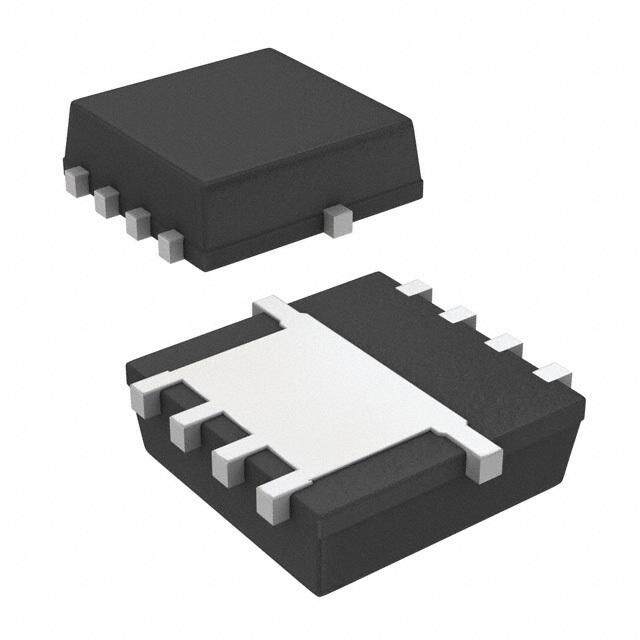
| 供应商器件封装 | 8-MLP(3.3X3.3),Power33 |
| 其它名称 | FDMC86106LZCT |
| 功率-最大值 | 2.3W |
| 包装 | 剪切带 (CT) |
| 商标 | Fairchild Semiconductor |
| 安装类型 | 表面贴装 |
| 安装风格 | SMD/SMT |
| 封装 | Reel |
| 封装/外壳 | 8-PowerWDFN |
| 封装/箱体 | MLP-8 3.3x3.3 |
| 工厂包装数量 | 3000 |
| 晶体管极性 | N-Channel |
| 最大工作温度 | + 150 C |
| 标准包装 | 1 |
| 正向跨导-最小值 | 11 S |
| 漏源极电压(Vdss) | 100V |
| 电流-连续漏极(Id)(25°C时) | 3.3A (Ta), 7.5A (Tc) |
| 系列 | FDMC86106LZ |


- 商务部:美国ITC正式对集成电路等产品启动337调查
- 曝三星4nm工艺存在良率问题 高通将骁龙8 Gen1或转产台积电
- 太阳诱电将投资9.5亿元在常州建新厂生产MLCC 预计2023年完工
- 英特尔发布欧洲新工厂建设计划 深化IDM 2.0 战略
- 台积电先进制程称霸业界 有大客户加持明年业绩稳了
- 达到5530亿美元!SIA预计今年全球半导体销售额将创下新高
- 英特尔拟将自动驾驶子公司Mobileye上市 估值或超500亿美元
- 三星加码芯片和SET,合并消费电子和移动部门,撤换高东真等 CEO
- 三星电子宣布重大人事变动 还合并消费电子和移动部门
- 海关总署:前11个月进口集成电路产品价值2.52万亿元 增长14.8%


PDF Datasheet 数据手册内容提取
F D M C 8 November 2013 6 1 FDMC86106LZ 0 6 L N-Channel Shielded Gate PowerTrench® MOSFET Z N 100 V, 7.5 A, 103 mΩ - C Features General Description h a n (cid:132) Shielded Gate MOSFET Technology This N-Channel logic Level MOSFETs are produced using n Fairchild Semiconductor‘s advanced PowerTrench® process e (cid:132) Max r = 103 mΩ at V = 10 V, I = 3.3 A DS(on) GS D that incorporates Shielded Gate technology. This process has l S (cid:132) Max rDS(on) = 153 mΩ at VGS = 4.5 V, ID = 2.7 A been optimized for the on-state resistance and yet maintain h superior switching performance. G-S zener has been added to i (cid:132) HBM ESD protection level > 3 KV typical (Note 4) e enhance ESD voltage level. l d (cid:132) 100% UIL Tested e d (cid:132) RoHS Compliant Application G a (cid:132) DC - DC Conversion t e P o w e r Top Bottom T r e 8 7 6 5 D D D D n S D c h ® S D M O S D S F E G D T 1 2 3 4 G S S S MLP 3.3x3.3 MOSFET Maximum Ratings TA = 25 °C unless otherwise noted Symbol Parameter Ratings Units V Drain to Source Voltage 100 V DS V Gate to Source Voltage ±20 V GS Drain Current -Continuous (Package limited) T = 25 °C 7.5 C -Continuous (Silicon limited) T = 25 °C 9.6 I C A D -Continuous T = 25 °C (Note 1a) 3.3 A -Pulsed 15 E Single Pulse Avalanche Energy (Note 3) 12 mJ AS Power Dissipation T = 25 °C 19 P C W D Power Dissipation T = 25 °C (Note 1a) 2.3 A T , T Operating and Storage Junction Temperature Range -55 to +150 °C J STG Thermal Characteristics R Thermal Resistance, Junction to Case 6.5 θJC °C/W R Thermal Resistance, Junction to Ambient (Note 1a) 53 θJA Package Marking and Ordering Information Device Marking Device Package Reel Size Tape Width Quantity FDMC86106Z FDMC86106LZ Power 33 13 ’’ 12 mm 3000 units ©2011 Fairchild Semiconductor Corporation 1 www.fairchildsemi.com FDMC86106LZ Rev.C2
F D Electrical Characteristics T = 25 °C unless otherwise noted M J C Symbol Parameter Test Conditions Min Typ Max Units 8 6 Off Characteristics 1 0 6 BVDSS Drain to Source Breakdown Voltage ID = 250 μA, VGS = 0 V 100 V L ΔBV Breakdown Voltage Temperature Z DSS I = 250 μA, referenced to 25 °C 73 mV/°C ΔT Coefficient D N J - I Zero Gate Voltage Drain Current V = 80 V, V = 0 V 1 μA C DSS DS GS h IGSS Gate to Source Leakage Current VGS = ±20 V, VDS = 0 V ±10 μA a n On Characteristics n e l V Gate to Source Threshold Voltage V = V , I = 250 μA 1.0 1.8 2.2 V GS(th) GS DS D S ΔV Gate to Source Threshold Voltage h ΔTGS(th) Temperature Coefficient ID = 250 μA, referenced to 25 °C -6 mV/°C ie J l V = 10 V, I = 3.3 A 79 103 d GS D e r Static Drain to Source On Resistance V = 4.5 V, I = 2.7 A 105 153 mΩ d DS(on) GS D V = 10 V, I = 3.3 A, T = 125 °C 136 178 G GS D J a gFS Forward Transconductance VDS = 5 V, ID = 3.3 A 11 S t e Dynamic Characteristics P o C Input Capacitance 232 310 pF w iss Coss Output Capacitance Vf =D S1 =M 5H0z V, VGS = 0 V, 45 60 pF erT Crss Reverse Transfer Capacitance 2.4 5 pF r e Rg Gate Resistance 0.7 Ω n c h Switching Characteristics ® td(on) Turn-On Delay Time 4.5 10 ns M tr Rise Time VDD = 50 V, ID = 3.3 A, 1.3 10 ns O td(off) Turn-Off Delay Time VGS = 10 V, RGEN = 6 Ω 10 20 ns SF t Fall Time 1.4 10 ns E f T Q Total Gate Charge V = 0 V to 10 V 4 6 nC g(TOT) GS V = 50 V, Q Total Gate Charge V = 0 V to 4.5 V DD 2 3 nC g(TOT) GS I = 3.3 A Q Total Gate Charge D 0.8 nC gs Q Gate to Drain “Miller” Charge 0.7 nC gd Drain-Source Diode Characteristics V = 0 V, I = 3.3 A (Note 2) 0.85 1.3 V Source to Drain Diode Forward Voltage GS S V SD V = 0 V, I = 2 A (Note 2) 0.82 1.2 GS S t Reverse Recovery Time 33 54 ns rr I = 3.3 A, di/dt = 100 A/μs Q Reverse Recovery Charge F 23 38 nC rr NOTES: 1. RθJA is determined with the device mounted on a 1 in2 pad 2 oz copper pad on a 1.5 x 1.5 in. board of FR-4 material. RθJC is guaranteed by design while RθCA is determined by the user's board design. a.53 °C/W when mounted on a b.125 °C/W when mounted on 1 in2 pad of 2 oz copper a minimum pad of 2 oz copper GDDSS FSFS GDDSS FSFS 2. Pulse Test: Pulse Width < 300 μs, Duty cycle < 2.0%. 3. Starting TJ = 25 °C; N-ch: L = 1.0 mH, IAS = 5.0 A, VDD = 90 V, VGS = 10 V. 4. The diode connected between gate and source serves only as protection against ESD. No gate overvoltage rating is implied. ©2011 Fairchild Semiconductor Corporation 2 www.fairchildsemi.com FDMC86106LZ Rev.C2
F D Typical Characteristics M T = 25 °C unless otherwise noted J C 8 6 15 5 1 VGS = 10 V VGS = 4.5 V CE VGS = 3 V 06 NT (A) 12 VGS = 4 V SISTAN 4 VGS = 3.5 V VGS = 4 V LZ N N CURRE 9 VGS = 3.5 V MALIZEDCE ON-RE 3 VGS = 4.5 V -Chan I, DRAID 36 PDUULTSYE C DYUCRLEA T=I O0.N5 %= 8M0A μXs VGS = 3 V NORTO SOUR 12 nel S RAIN PDUULTSYE C DYUCRLEA T=I O0.N5 %= 8M0A μXs VGS = 10 V hie 00 1 2 3 4 5 D 00 3 6 9 12 15 ld e V , DRAIN TO SOURCE VOLTAGE (V) ID, DRAIN CURR ENT (A) d DS G a Figure 1. On Region Characteristics Figure 2. Normalized On-Resistance t e vs Drain Current and Gate Voltage P o w 2.2 500 e NORMALIZED O SOURCE ON-RESISTANCE 111112......024680 VIDG =S 3=. 31 0A V rDRAIN TO ,DS(on)()mCE ON-RESISTANCE Ω234000000 ID = 3.3 A PDUUTLTJSY =E C1 DY25UC RLoCEA T=I O0.N5 %= 8M0A μXs rTrenchMOSF® RAIN T 0.8 SOUR100 TJ = 25 oC ET D 0.6 0 -75 -50 -25 0 25 50 75 100 125 150 2 4 6 8 10 TJ, JUNCTION TEM PERATURE (oC) VGS, GATE TO SOURCE VOLTAGE (V) Figure 3. Normalized On Resistance Figure 4. On-Resistance vs Gate to vs Junction Temperature Source Voltage 15 20 PULSE DURATION = 80 μs A) 10 VGS = 0 V DUTY CYCLE = 0.5% MAX T ( 12 N E RRENT (A) 9 VDS = 5 V AIN CURR 1 TJ = 150 oC CU DR 0.1 I, DRAIN D 36 TJ = 150 oC TJ = 25 oC , REVERSE S 0.01 TJ = T-5J 5= o2C5 oC TJ = -55 oC I 0 0.001 1 2 3 4 5 6 0.0 0.2 0.4 0.6 0.8 1.0 1.2 VGS, GATE TO SOU RCE VOLTAGE (V) VSD, BODY DIODE FOR WARD VOLTAGE (V) Figure 5. Transfer Characteristics Figure 6. Source to Drain Diode Forward Voltage vs Source Current ©2011 Fairchild Semiconductor Corporation 3 www.fairchildsemi.com FDMC86106LZ Rev.C2
F D M Typical Characteristics TJ = 25 °C unless otherwise noted C 8 6 1 10 1000 0 GE (V) 8 ID = 3.3 A VDD = 25 V 6LZ SOURCE VOLTA 46 VDD = 75 VVDD = 50 V CITANCE (pF) 100 CCoissss N-Chann O PA 10 e E T CA l S T 2 A h V, GGS 0 1 fV =G S1 =M 0H Vz Crss ield 0 1 2 3 4 5 0.1 1 10 100 e d Qg, GATE CH ARGE (nC) VDS, DRAIN TO SOU RCE VOLTAGE (V) G a Figure 7. Gate Charge Characteristics Figure 8. Capacitance vs Drain te to Source Voltage P o w e 10 10-1 r 9 T , AVALANCHE CURRENT (A)S 2345678 TJ = 12T5J o=C 25T oJC = 100 oC GATE LEAKAGE CURRENT (A)11111110000000-------8765432 VGS = 0 V TJ = 125 oC TJ = 25 oC renchMOSFET® IA , g 1 I10-9 0.001 0.01 0.1 1 10 0 4 8 12 16 20 24 28 32 36 tAV, TIME IN AVA LANCHE (ms) VGS, GATE TO S OURCE VOLTAGE (V) Figure 9. Unclamped Inductive Figure 10. Gate Leakage Current vs Gate to Switching Capability Source Voltage 10 20 10 NT (A) 8 T (A) 100 us , IDRAIN CURRED 246 Limited by package VGS =V G4S.5 = V 10 V I, DRAIN CURREND 0.11 TLSTRIHJIθMN JI=SAIG T M =LAE AER1DX 2E PB 5ARU Yo ALCI SrST/DW EESD(on) 111110 0 0sm 0 sm smss RθJC = 6.5 oC/W 0.01 TA = 25 oC DC 0 0.005 25 50 75 100 125 150 0.1 1 10 100 400 TC, CASE TEMPERATURE (oC) VDS, DRAIN to SOU RCE VOLTAGE (V) Figure 11. Maximum Continuous Drain Figure 12. Forward Bias Safe Current vs Case Temperature Operating Area ©2011 Fairchild Semiconductor Corporation 4 www.fairchildsemi.com FDMC86106LZ Rev.C2
F D Typical Characteristics T = 25 °C unless otherwise noted M J C 8 500 6 1 0 W) 6 L R ( 100 Z WE N O P - T C EN h NSI 10 an A R n EAK T SRIθNJAG =L E1 2P5U oLCS/EW el S , PPK) 1 TA = 25 oC hie P( l 0.5 d 10-4 10-3 10-2 10-1 1 10 100 1000 e d t, PULSE WIDTH (s ec) G Figure 13. Single Pulse Maximum Power Dissipation a t e P 2 o 1 DUTY CYCLE-DESCENDING ORDER w e r T THERMAL ZE,JAθ 0.1 D = 000...215 PDM rench NORMALIZED IMPEDANC 0.01 000...000521 SRIθNJAG =L E1 2P5U oLCS/WE NDPEOUATTYKE S FT:AJ C= TPODRM: xD Z =θ JtA1 /xt2 RθJAt1 +t T2A MOSFET® 0.001 10-4 10-3 10-2 10-1 1 10 100 1000 t, RECTANGULAR PULSE DURATION (sec) Figure 14. Junction-to-Ambient Transient Thermal Response Curve ©2011 Fairchild Semiconductor Corporation 5 www.fairchildsemi.com FDMC86106LZ Rev.C2
F D M Dimensional Outline and Pad Layout C 8 6 0.10 C (cid:22)(cid:17)(cid:22)(cid:19)(cid:147)(cid:19)(cid:17)(cid:20)(cid:19) A (3.40) 10 2.37 6 2X B 8 5 L Z 0.45(4X) N - C 2.15 h a (1.70) n n e (0.40) l (cid:22)(cid:17)(cid:22)(cid:19)(cid:147)(cid:19)(cid:17)(cid:20)(cid:19) S h KEEP OUT i AREA e l (0.65) d 0.70(4X) e d PIN1 1 4 G IDENT 0.10 C 0.65 0.42(8X) a TOP VIEW t 1.95 e 2X P o w e A 0.8MAX rT r e n c (cid:20)(cid:20)(cid:131)(cid:48)(cid:36)(cid:59) h 0.10 C ® (0.20) M O S 0.08 C 0.05 RECOMMENDED LAND PATTERN F 0.00 E SIDE VIEW C T NOTES: SEATING PLANE A.EXCEPT AS NOTED, PACKAGE CONFORMS TO JEDEC REGISTRATION MO-240 VARIATION BA.. B.DIMENSIONS ARE IN MILLIMETERS. 2.27+0.05 C.DIMENSIONS AND TOLERANCES PER ASME Y14.5M,1994. D.SEATING PLANE IS DEFINED BY TERMINAL TIPS ONLY 1 4 E.BODY DIMENSIONS DO NOT INCLUDE MOLD FLASH 0.45+0.05 PROTRUSIONS NOR GATEBURRS. (4X) (0.40) F.FLANGE DIMENSIONS INCLUDE INTERTERMINAL FLASH (1.20) OR PROTRUSION. INTERTERMINAL FLASH OR PROTRUSION SHALL NOT EXCEED 0.25MM PER SIDE. G.IT IS RECOMMENDED TO HAVE NO TRACES OR VIA 2.05+0.05 WITHIN THE KEEP OUT AREA. 0.45+0.05 H.DRAWING FILENAME: MKT-MLP08Trev3. (3X) A I.GENERAL RADII FOR ALL CORNERS SHALL BE 0.20MM MAX. 8 5 J.FAIRCHILD SEMICONDUCTOR. 0.32+0.05(8X) 0.65 0.10 C A B 1.95 0.05 C BOTTOM VIEW ©2011 Fairchild Semiconductor Corporation 6 www.fairchildsemi.com FDMC86106LZ Rev.C2
F D M C 8 6 1 0 6 TRADEMARKS L Z The following includes registered and unregistered trademarks and service marks, owned by Fairchild Semiconductor and/or its global subsidiaries, and is not N intended to be an exhaustive list of all such trademarks. - AccuPower™ F-PFS™ Sync-Lock™ C AX-CAP®* FRFET® ® ®* h BitSiC™ Global Power ResourceSM PowtmerTrench® a BCCuooirrleedPP itOL NUWoSEw™R™™ GGGrrreeeeeennnB FFrPPidSSg™™e™ e-Series™ PPQorFowEgeTrar®XmSm™able Active Droop™ TTiinnyyBBouocks®t® nne CROSSVOLT™ Gmax™ QS™ TTiinnyyCLoaglcic™® l S CTL™ GTO™ Quiet Series™ TINYOPTO™ h CDDuuEarUrle XCnPot EoTElr™aDn®sfer Logic™ IIMnStaOerlPkliiMLnAgA NSXAm™Ra™ll Speakers Sound Louder Rapid™Configure™ TTiinnyyPPoWwMe™r™ ield EcoSPARK® and Better™ Saving our world, 1mW/W/kW at a time™ TinyWire™ e TranSiC™ d EfficentMax™ MegaBuck™ SignalWise™ TriFault Detect™ ESBC™ MICROCOUPLER™ SmartMax™ TRUECURRENT®* G ® MicroFET™ SMART START™ μSerDes™ a MicroPak™ Solutions for Your Success™ t e Fairchild® MicroPak2™ SPM® FFFAAaiCCrcTTh® iQldu Sieet mSiecroiensd™uctor® MMmiWollteiSorDanvMrievarex®™™ SSSTuuppEeeArrLSFTEOHTT™®™-3 UUHltrCa ®FRFET™ Pow FFaAsStTvC®ore™ OOpPtToOHLiTO™GIC® SSuuppeerrSSOOTT™™--68 UVCniXF™ET™ erT FETBench™ OPTOPLANAR® SupreMOS® VisualMax™ r FPS™ SyncFET™ VXoSl™tagePlus™ en c h ® *Trademarks of System General Corporation, used under license by Fairchild Semiconductor. M DISCLAIMER O FAIRCHILD SEMICONDUCTOR RESERVES THE RIGHT TO MAKE CHANGES WITHOUT FURTHER NOTICE TO ANY PRODUCTS HEREIN TO IMPROVE RELIABILITY, FUNCTION, OR DESIGN. FAIRCHILD DOES NOT ASSUME ANY LIABILITY ARISING OUT OF THE APPLICATION OR USE OF ANY S PRODUCT OR CIRCUIT DESCRIBED HEREIN; NEITHER DOES IT CONVEY ANY LICENSE UNDER ITS PATENT RIGHTS, NOR THE RIGHTS OF OTHERS. F E THESE SPECIFICATIONS DO NOT EXPAND THE TERMS OF FAIRCHILD’S WORLDWIDE TERMS AND CONDITIONS, SPECIFICALLY THE WARRANTY T THEREIN, WHICH COVERS THESE PRODUCTS. LIFE SUPPORT POLICY FAIRCHILD’S PRODUCTS ARE NOT AUTHORIZED FOR USE AS CRITICAL COMPONENTS IN LIFE SUPPORT DEVICES OR SYSTEMS WITHOUT THE EXPRESS WRITTEN APPROVAL OF FAIRCHILD SEMICONDUCTOR CORPORATION. As used here in: 1. Life support devices or systems are devices or systems which, (a) are 2. A critical component in any component of a life support, device, or intended for surgical implant into the body or (b) support or sustain life, system whose failure to perform can be reasonably expected to cause and (c) whose failure to perform when properly used in accordance with the failure of the life support device or system, or to affect its safety or instructions for use provided in the labeling, can be reasonably effectiveness. expected to result in a significant injury of the user. ANTI-COUNTERFEITING POLICY Fairchild Semiconductor Corporation’s Anti-Counterfeiting Policy. Fairchild’s Anti-Counterfeiting Policy is also stated on our external website, www.Fairchildsemi.com, under Sales Support. Counterfeiting of semiconductor parts is a growing problem in the industry. All manufactures of semiconductor products are experiencing counterfeiting of their parts. Customers who inadvertently purchase counterfeit parts experience many problems such as loss of brand reputation, substandard performance, failed application, and increased cost of production and manufacturing delays. Fairchild is taking strong measures to protect ourselves and our customers from the proliferation of counterfeit parts. Fairchild strongly encourages customers to purchase Fairchild parts either directly from Fairchild or from Authorized Fairchild Distributors who are listed by country on our web page cited above. Products customers buy either from Fairchild directly or from Authorized Fairchild Distributors are genuine parts, have full traceability, meet Fairchild’s quality standards for handing and storage and provide access to Fairchild’s full range of up-to-date technical and product information. Fairchild and our Authorized Distributors will stand behind all warranties and will appropriately address and warranty issues that may arise. Fairchild will not provide any warranty coverage or other assistance for parts bought from Unauthorized Sources. Fairchild is committed to combat this global problem and encourage our customers to do their part in stopping this practice by buying direct or from authorized distributors. PRODUCT STATUS DEFINITIONS Definition of Terms Datasheet Identification Product Status Definition Datasheet contains the design specifications for product development. Specifications Advance Information Formative / In Design may change in any manner without notice. Datasheet contains preliminary data; supplementary data will be published at a later Preliminary First Production date. Fairchild Semiconductor reserves the right to make changes at any time without notice to improve design. Datasheet contains final specifications. Fairchild Semiconductor reserves the right to No Identification Needed Full Production make changes at any time without notice to improve the design. Datasheet contains specifications on a product that is discontinued by Fairchild Obsolete Not In Production Semiconductor. The datasheet is for reference information only. Rev. I66 ©2011 Fairchild Semiconductor Corporation 7 www.fairchildsemi.com FDMC86106LZ Rev.C2