ICGOO在线商城 > 分立半导体产品 > 晶体管 - FET,MOSFET - 单 > IRFB7446PBF
/IRFB7446PBF.jpg)
 Datasheet下载
- 型号: IRFB7446PBF
- 制造商: International Rectifier
- 库位|库存: xxxx|xxxx
- 要求:
| 数量阶梯 | 香港交货 | 国内含税 |
| +xxxx | $xxxx | ¥xxxx |
查看当月历史价格
查看今年历史价格
IRFB7446PBF产品简介:
ICGOO电子元器件商城为您提供IRFB7446PBF由International Rectifier设计生产,在icgoo商城现货销售,并且可以通过原厂、代理商等渠道进行代购。 IRFB7446PBF价格参考¥6.35-¥6.35。International RectifierIRFB7446PBF封装/规格:晶体管 - FET,MOSFET - 单, 通孔 N 沟道 40V 120A(Tc) 99W(Tc) TO-220AB。您可以下载IRFB7446PBF参考资料、Datasheet数据手册功能说明书,资料中有IRFB7446PBF 详细功能的应用电路图电压和使用方法及教程。
Infineon Technologies(英飞凌科技)生产的型号为IRFB7446PBF的晶体管属于FET(场效应晶体管)、MOSFET(金属氧化物半导体场效应晶体管)类别,且为单通道设计。该器件的应用场景广泛,主要集中在需要高效功率转换、开关和控制的领域。以下是其典型应用场景:

1. 电源管理:
   IRFB7446PBF常用于开关电源(SMPS)、DC-DC转换器和AC-DC转换器中,作为功率开关元件。它能够实现高效的电压转换和稳定的电流输出,适用于消费电子、工业设备和通信设备中的电源模块。

2. 电机驱动:
   在小型电机驱动应用中,该MOSFET可用于控制电机的速度和方向。例如,家用电器(如风扇、水泵)或工业自动化设备中的直流无刷电机(BLDC)驱动电路。

3. 负载切换:
   该器件可作为负载切换开关,用于控制高电流负载的通断。例如,在汽车电子系统中,用于控制车灯、雨刷或空调系统的电源供应。

4. 电池管理系统(BMS):
   在电池保护和管理系统中,IRFB7446PBF可用于电池充放电路径的控制,确保电池在安全的工作范围内运行,并防止过流、短路等问题。

5. 逆变器:
   在光伏逆变器或其他类型的逆变器中,该MOSFET可用作高频开关元件,将直流电转换为交流电,以供家庭或工业用电需求。

6. LED驱动:
   高亮度LED照明系统中,该器件可作为恒流源的一部分,用于精确调节LED的亮度和颜色。

7. 电信设备:
   在基站、路由器和其他电信设备中,IRFB7446PBF可用于功率放大器的偏置电路或辅助电源电路中。

8. 工业自动化:
   该MOSFET可用于可编程逻辑控制器(PLC)、传感器接口和执行器驱动等工业自动化场景,提供可靠的开关和控制功能。

总之,IRFB7446PBF凭借其低导通电阻(Rds(on))、高开关速度和良好的热性能,成为许多功率电子应用的理想选择,尤其适合需要高效能和稳定性的场合。
| 参数 | 数值 |
| 产品目录 | |
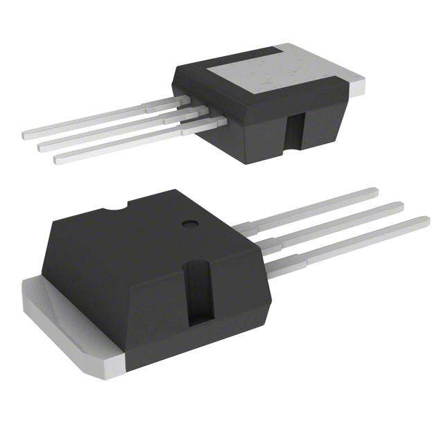
| 描述 | MOSFET N CH 40V TO220MOSFET 40V 118A 3.3 mOhm HEXFET 62nC 99W |
| 产品分类 | FET - 单分离式半导体 |
| FET功能 | 标准 |
| FET类型 | MOSFET N 通道,金属氧化物 |
| Id-ContinuousDrainCurrent | 123 A |
| Id-连续漏极电流 | 123 A |
| 品牌 | International Rectifier |
| 产品手册 | |
| 产品图片 |
|
| rohs | 符合RoHS无铅 / 符合限制有害物质指令(RoHS)规范要求 |
| 产品系列 | 晶体管,MOSFET,International Rectifier IRFB7446PBFHEXFET®, StrongIRFET™ |
| 数据手册 | |
| 产品型号 | IRFB7446PBF |
| PCN组件/产地 | |
| Pd-PowerDissipation | 99 W |
| Pd-功率耗散 | 99 W |
| Qg-GateCharge | 93 nC |
| Qg-栅极电荷 | 93 nC |
| RdsOn-Drain-SourceResistance | 3.3 mOhms |
| RdsOn-漏源导通电阻 | 3.3 mOhms |
| Vds-Drain-SourceBreakdownVoltage | 40 V |
| Vds-漏源极击穿电压 | 40 V |
| Vgs-Gate-SourceBreakdownVoltage | 20 V |
| Vgs-栅源极击穿电压 | 20 V |
| 不同Id时的Vgs(th)(最大值) | 3.9V @ 100µA |
| 不同Vds时的输入电容(Ciss) | 3183pF @ 25V |
| 不同Vgs时的栅极电荷(Qg) | 93nC @ 10V |
| 不同 Id、Vgs时的 RdsOn(最大值) | 3.3 毫欧 @ 70A,10V |
| 产品培训模块 | http://www.digikey.cn/PTM/IndividualPTM.page?site=cn&lang=zhs&ptm=26250http://www.digikey.cn/PTM/IndividualPTM.page?site=cn&lang=zhs&ptm=26240 |
| 产品种类 | MOSFET |
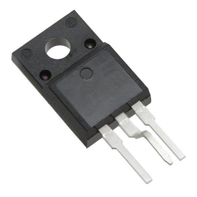
| 供应商器件封装 | TO-220AB |
| 功率-最大值 | 99W |
| 功率耗散 | 99 W |
| 包装 | 管件 |
| 商标 | International Rectifier |
| 商标名 | StrongIRFET |
| 安装类型 | 通孔 |
| 安装风格 | Through Hole |
| 导通电阻 | 3.3 mOhms |
| 封装 | Tube |
| 封装/外壳 | TO-220-3 |
| 封装/箱体 | TO-220-3 |
| 工厂包装数量 | 50 |
| 晶体管极性 | N-Channel |
| 栅极电荷Qg | 93 nC |
| 标准包装 | 50 |
| 汲极/源极击穿电压 | 40 V |
| 漏极连续电流 | 123 A |
| 漏源极电压(Vdss) | 40V |
| 特色产品 | http://www.digikey.com/product-highlights/cn/zh/international-rectifier-strongirfet-power-mosfet/2963 |
| 电流-连续漏极(Id)(25°C时) | 120A (Tc) |
| 设计资源 | http://www.irf.com/product-info/models/saber/irfb7446pbf.sinhttp://www.irf.com/product-info/models/spice/irfb7446pbf.spi |
| 闸/源击穿电压 | 20 V |


- 商务部:美国ITC正式对集成电路等产品启动337调查
- 曝三星4nm工艺存在良率问题 高通将骁龙8 Gen1或转产台积电
- 太阳诱电将投资9.5亿元在常州建新厂生产MLCC 预计2023年完工
- 英特尔发布欧洲新工厂建设计划 深化IDM 2.0 战略
- 台积电先进制程称霸业界 有大客户加持明年业绩稳了
- 达到5530亿美元!SIA预计今年全球半导体销售额将创下新高
- 英特尔拟将自动驾驶子公司Mobileye上市 估值或超500亿美元
- 三星加码芯片和SET,合并消费电子和移动部门,撤换高东真等 CEO
- 三星电子宣布重大人事变动 还合并消费电子和移动部门
- 海关总署:前11个月进口集成电路产品价值2.52万亿元 增长14.8%


PDF Datasheet 数据手册内容提取
StrongIRFET™ IRFB7446PbF Application HEXFET® Power MOSFET Brushed Motor drive applications BLDC Motor drive applications D VDSS 40V R typ. 2.6m Battery powered circuits DS(on) Half-bridge and full-bridge topologies max 3.3m Synchronous rectifier applications G I 123A Resonant mode power supplies D (Silicon Limited) OR-ing and redundant power switches S I 120A D (Package Limited) DC/DC and AC/DC converters DC/AC Inverters Benefits S Improved Gate, Avalanche and Dynamic dV/dt Ruggedness D G Fully Characterized Capacitance and Avalanche SOA TO-220AB Enhanced body diode dV/dt and dI/dt Capability IRFB7446PbF Lead-Free* RoHS Compliant, Halogen-Free* G D S Gate Drain Source Base part number Package Type Standard Pack Orderable Part Number Form Quantity IRFB7446PbF TO-220 Tube 50 IRFB7446PbF ) 8 125 m (e ID = 70A c n a 100 st 6 si eORn TJ = 125°C )An(t e 75 ce 4 urr uro Cn S- o ariD 50 ani-t 2 ,D Dr I , n) TJ = 25°C 25 o (S RD 0 0 2 4 6 8 10 12 14 16 18 20 25 50 75 100 125 150 175 VGS, Gate -to -Source Voltage (V) TC , Case Temperature (°C) Fig 1. Typical On-Resistance vs. Gate Voltage Fig 2. Maximum Drain Current vs. Case Temperature 1 www.irf.com © 2014 International Rectifier Submit Datasheet Feedback November 7, 2014
IRFB7446PbF Absolute Maximum Rating Symbol Parameter Max. Units I @ T = 25°C Continuous Drain Current, VGS @ 10V (Silicon Limited) 123 D C I @ T = 100°C Continuous Drain Current, V @ 10V (Silicon Limited) 87 D C GS A I @ T = 25°C Continuous Drain Current, V @ 10V (Wire Bond Limited) 120 D C GS I Pulsed Drain Current 492 DM P @T = 25°C Maximum Power Dissipation 99 W D C Linear Derating Factor 0.66 W/°C V Gate-to-Source Voltage ± 20 V GS T Operating Junction and J -55 to + 175 T Storage Temperature Range °C STG Soldering Temperature, for 10 seconds (1.6mm from case) 300 Mounting Torque, 6-32 or M3 Screw 10 lbf·in (1.1 N·m) Avalanche Characteristics E Single Pulse Avalanche Energy 111 AS mJ EAS (L=1mH) Single Pulse Avalanche Energy 236 I Avalanche Current A AR See Fig 15, 16, 23a, 23b E Repetitive Avalanche Energy mJ AR Thermal Resistance Symbol Parameter Typ. Max. Units R Junction-to-Case ––– 1.52 JC R Case-to-Sink, Flat Greased Surface 0.50 ––– °C/W CS R Junction-to-Ambient ––– 62 JA Static @ T = 25°C (unless otherwise specified) J Symbol Parameter Min. Typ. Max. Units Conditions V Drain-to-Source Breakdown Voltage 40 ––– ––– V V = 0V, I = 250µA (BR)DSS GS D V /T Breakdown Voltage Temp. Coefficient ––– 0.033 ––– V/°C Reference to 25°C, I = 5mA (BR)DSS J D ––– 2.6 3.3 V = 10V, I = 70A R Static Drain-to-Source On-Resistance m GS D DS(on) ––– 3.9 ––– V = 6.0V, I = 35A GS D V Gate Threshold Voltage 2.2 3.0 3.9 V V = V , I = 100µA GS(th) DS GS D ––– ––– 1.0 V =40 V, V = 0V I Drain-to-Source Leakage Current µA DS GS DSS ––– ––– 150 V =40V,V = 0V,T =125°C DS GS J Gate-to-Source Forward Leakage ––– ––– 100 V = 20V I nA GS GSS Gate-to-Source Reverse Leakage ––– ––– -100 V = -20V GS R Gate Resistance ––– 1.6 ––– G Notes: Calculated continuous current based on maximum allowable junction temperature. Bond wire current limit is 120A. Note that current limitations arising from heating of the device leads may occur with some lead mounting arrangements. (Refer to AN-1140) Repetitive rating; pulse width limited by max. junction temperature. Limited by T , starting T = 25°C, L = 0.046mH,R = 50, I = 70A, V =10V. Jmax J G AS GS I 70A, di/dt 1174A/µs, V V , T 175°C. SD DD (BR)DSS J Pulse width 400µs; duty cycle 2%. C eff. (TR) is a fixed capacitance that gives the same charging time as C while V is rising from 0 to 80% V . oss oss DS DSS C eff. (ER) is a fixed capacitance that gives the same energy as C while VDS is rising from 0 to 80% V . oss oss DSS R is measured at T approximately 90°C. J This value determined from sample failure population, starting T = 25°C, L= 1mH, R = 50, I = 22A, V =10V. J G AS GS * Halogen -Free since April 30, 2014 2 www.irf.com © 2014 International Rectifier Submit Datasheet Feedback November 7, 2014
IRFB7446PbF Dynamic Electrical Characteristics @ T = 25°C (unless otherwise specified) J Symbol Parameter Min. Typ. Max. Units Conditions gfs Forward Transconductance 269 ––– ––– S V = 10V, I =70A DS D Q Total Gate Charge ––– 62 93 I = 70A g D Q Gate-to-Source Charge ––– 16 ––– V = 20V gs nC DS Q Gate-to-Drain Charge ––– 20 ––– V = 10V gd GS Q Total Gate Charge Sync. (Qg– Qgd) ––– 42 ––– sync t Turn-On Delay Time ––– 11 ––– V = 20V d(on) DD t Rise Time ––– 34 ––– I = 30A r D ns t Turn-Off Delay Time ––– 33 ––– R = 2.7 d(off) G t Fall Time ––– 23 ––– V = 10V f GS C Input Capacitance ––– 3183 ––– V = 0V iss GS C Output Capacitance ––– 475 ––– V = 25V oss DS C Reverse Transfer Capacitance ––– 331 ––– ƒ = 1.0MHz, See Fig.5 rss pF Effective Output Capacitance C ––– 596 ––– V = 0V, VDS = 0V to 32V oss eff.(ER) (Energy Related) GS C Output Capacitance (Time Related) ––– 688 ––– V = 0V, VDS = 0V to 32V oss eff.(TR) GS Diode Characteristics Symbol Parameter Min. Typ. Max. Units Conditions Continuous Source Current MOSFET symbol D I ––– ––– 120 S (Body Diode) showing the A Pulsed Source Current integral reverse G I ––– ––– 492 SM (Body Diode) p-n junction diode. S V Diode Forward Voltage ––– 0.9 1.3 V T = 25°C,I = 70A,V = 0V SD J S GS dv/dt Peak Diode Recovery dv/dt ––– 7.6 ––– V/ns T = 175°C,I = 70A,V = 40V J S DS ––– 22 ––– T = 25°C V = 34V t Reverse Recovery Time ns J DD rr ––– 24 ––– T = 125°C I = 70A, J F ––– 15 ––– T = 25°C di/dt = 100A/µs J Q Reverse Recovery Charge nC rr ––– 15 ––– T = 125°C J I Reverse Recovery Current ––– 1.0 ––– A T = 25°C RRM J 3 www.irf.com © 2014 International Rectifier Submit Datasheet Feedback November 7, 2014
IRFB7446PbF 1000 1000 VGS VGS TOP 15V TOP 15V 10V 10V )An(t 100 876...000VVV A)n(t 876...000VVV eurrC BOTTOM 554...505VVV eCurr100 BOTTOM 554...505VVV e e cru 10 ucr o o S S -o o- 4.5V n-t tn- 10 ai 4.5V ai Dr 1 rD , D , D I 60µs PULSE WIDTH I 60µs PULSE WIDTH Tj = 25°C Tj = 175°C 0.1 1 0.1 1 10 100 0.1 1 10 100 VDS, Drain-to-Source Voltage (V) VDS, Drain-to-Source Voltage (V) Fig 3. Typical Output Characteristics Fig 4. Typical Output Characteristics 1000 2.2 e cn ID = 70A )A(t n 100 TJ = 175°C ssaitRe 1.8 VGS = 10V erru n O Ce Soucrno--tDa ri,ID 01.011 TJ =V 26D50S°µC s= P 1U0LVSE WIDTH ce Sourno--tDa ri,R on()DSed)mazliNo( r 11..04 0.6 2 4 6 8 10 -60 -20 20 60 100 140 180 VGS, Gate-to-Source Voltage (V) TJ , Junction Temperature (°C) Fig 5. Typical Transfer Characteristics Fig 6. Normalized On-Resistance vs. Temperature 100000 14.0 VGS = 0V, f = 1 MHZ Ciss = Cgs + Cgd, Cds SHORTED ID= 70A 12.0 Fp)( ance 10000 CCrossss == CCdgsd + Cgd Ciss Ve)( oagltVce ur 108..00 VVDDSS== 3220VV cit So pa o- 6.0 Ca Coss e-t , C 1000 Crss Ga, tS 4.0 G V 2.0 100 0.0 0.1 1 10 100 0 10 20 30 40 50 60 70 80 VDS, Drain-to-Source Voltage (V) QG, Total Gate Charge (nC) Fig 8. Typical Gate Charge vs. Fig 7. Typical Capacitance vs. Drain-to-Source Voltage Gate-to-Source Voltage 4 www.irf.com © 2014 International Rectifier Submit Datasheet Feedback November 7, 2014
IRFB7446PbF 1000 10000 OPERATION IN THIS AREA LIMITED BY R (on) DS )Ant( 100 TJ = 175°C )Aen(t 1000 eurr Curr 100µsec Canri Dse 10 TJ = 25°C ucer Soo- 11000 Package Limited DC 1msec reve an-it 10msec R, DS 1 D, rD 1 Tc = 25°C I I Tj = 175°C VGS = 0V Single Pulse 0.1 0.1 0.0 0.5 1.0 1.5 2.0 0.1 1 10 100 VSD, Source-to-Drain Voltage (V) VDS, Drain-to-Source Voltage (V) Fig 10. Maximum Safe Operating Area Fig 9. Typical Source-Drain Diode Forward Voltage V) 50 0.6 ( age 49 Id = 5.0mA VDS= 0V to 32V lto 0.5 V n 48 w do 47 0.4 k a eBr 46 µJ) ucer 45 ( egyr 0.3 So 44 nE o- 0.2 n-t 43 ai rD 42 ,S 0.1 S 41 D R) B 40 0.0 V( -60 -20 20 60 100 140 180 0 5 10 15 20 25 30 35 40 45 TJ , Temperature ( °C ) VDS, Drain-to-Source Voltage (V) Fig 11. Drain-to-Source Breakdown Voltage Fig 12. Typical C Stored Energy oss ) 20.0 m (e VGS = 5.5V c n VGS = 6.0V a st 15.0 VGS = 7.0V sie VGS = 8.0V R VGS = 10V n O e cru 10.0 o S -o n-t iDar 5.0 n), o (S D R 0.0 0 100 200 300 400 500 I , Drain Current (A) D Fig 13. Typical On-Resistance vs. Drain Current 5 www.irf.com © 2014 International Rectifier Submit Datasheet Feedback November 7, 2014
IRFB7446PbF 10 W /C °) C 1 D = 0.50 J h 0.20 t Z ( e s 0.1 00..1005 n o p 0.02 s eR 0.01 la m 0.01 reh SINGLE PULSE Notes: T ( THERMAL RESPONSE ) 1. Duty Factor D = t1/t2 2. Peak Tj = P dm x Zthjc + Tc 0.001 1E-006 1E-005 0.0001 0.001 0.01 0.1 t , Rectangular Pulse Duration (sec) 1 Fig 14. Maximum Effective Transient Thermal Impedance, Junction-to-Case 1000 Allowed avalanche Current vs avalanche pulsewidth, tav, assuming Tj = 150°C and 100 Tstart = 25°C (Single Pulse) )A ( nt e rru C 10 e h c n a la v A 1 Allowed avalanche Current vs avalanche pulsewidth, tav, assuming j = 25°C and Tstart = 150°C. 0.1 1.0E-06 1.0E-05 1.0E-04 1.0E-03 1.0E-02 1.0E-01 tav (sec) Fig 15. Avalanche Current vs. Pulse Width 120 TOP Single Pulse Notes on Repetitive Avalanche Curves , Figures 15, 16: BOTTOM 1.0% Duty Cycle (For further info, see AN-1005 at www.irf.com) )J ID = 70A 1.Avalanche failures assumption: m Purely a thermal phenomenon and failure occurs at a ( y temperature far in excess of T . This is validated for every g 80 jmax er part type. n E 2. Safe operation in Avalanche is allowed as long asT is not e h exceeded. jmax nc 3. Equation below based on circuit and waveforms shown in Figures a la 23a, 23b. Av, R 40 45.. PBDV ( a=v eR) =a tAevde braregaek pdoowwenr vdoisltsaigpea t(i1o.n3 pfaecr tsoirn galcec oauvanltasn fcohr ev oplutalsgee. A increase during avalanche). E 6. I = Allowable avalanche current. av 7. T = Allowable rise in junction temperature, not to exceed T jmax (assumed as 25°C in Figure 14, 15). 0 t = Average time in avalanche. av 25 50 75 100 125 150 175 D = Duty cycle in avalanche = tav ·f Z (D, t ) = Transient thermal resistance, see Figures 14) Starting TJ , Junction Temperature (°C) thJC av PD (ave) = 1/2 ( 1.3·BV·I ) = T/ Z av thJC I = 2T/ [1.3·BV·Z ] av th Fig 16. Maximum Avalanche Energy vs. Temperature EAS (AR) = PD (ave)·tav 6 www.irf.com © 2014 International Rectifier Submit Datasheet Feedback November 7, 2014
IRFB7446PbF 4.5 6 IF = 46A V)(age 3.5 5 VTJR = = 2 354°VC tVol 4 TJ = 125°C d shole 2.5 A)( M 3 hr R taet ID = 100µA IR G ID = 250µA 2 , )h 1.5 ID = 1.0mA S(t ID = 1.0A G 1 V 0.5 0 -75 -25 25 75 125 175 225 0 200 400 600 800 1000 T , Temperature ( °C ) di /dt (A/µs) J F Fig 17. Threshold Voltage vs. Temperature Fig 18. Typical Recovery Current vs. dif/dt 5 70 IF = 70A IF = 46A VR = 34V 60 VR = 34V 4 TJ = 25°C TJ = 25°C 50 TJ = 125°C TJ = 125°C A) 3 )C 40 ( RM n( R R R 30 I 2 Q 20 1 10 0 0 0 200 400 600 800 1000 0 200 400 600 800 1000 diF /dt (A/µs) diF /dt (A/µs) Fig 19. Typical Recovery Current vs. dif/dt Fig 20. Typical Stored Charge vs. dif/dt 60 IF = 70A V = 34V 50 R T = 25°C J T = 125°C 40 J )C n ( R 30 R Q 20 10 0 0 200 400 600 800 1000 di /dt (A/µs) F Fig 21. Typical Stored Charge vs. dif/dt 7 www.irf.com © 2014 International Rectifier Submit Datasheet Feedback November 7, 2014
IRFB7446PbF Fig 22. Peak Diode Recovery dv/dt Test Circuit for N-Channel HEXFET® Power MOSFETs V(BR)DSS tp 15V VDS L DRIVER RG D.U.T + - VDD IAS A 20V tp 0.01 IAS Fig 23a. Unclamped Inductive Test Circuit Fig 23b. Unclamped Inductive Waveforms Fig 24a. Switching Time Test Circuit Fig 24b. Switching Time Waveforms Id Vds Vgs VDD Vgs(th) Qgs1 Qgs2 Qgd Qgodr Fig 25a. Gate Charge Test Circuit Fig 25b. Gate Charge Waveform 8 www.irf.com © 2014 International Rectifier Submit Datasheet Feedback November 7, 2014
IRFB7446PbF TO-220AB Package Outline (Dimensions are shown in millimeters (inches)) TO-220AB Part Marking Information EXAM PLE: THIS IS AN IRF1010 LO T CO DE 1789 INTERNATIO NAL PART NUM BER ASSEM BLED O N W W 19, 2000 RECTIFIER IN THE ASSEM BLY LINE "C" LO GO DATE CO DE YEAR 0 = 2000 Note: "P" in assem bly line position ASSEM BLY indicates "Lead - Free" LO T CO DE W EEK 19 LINE C TO-220AB packages are not recommended for Surface Mount Application. Note: For the most current drawing please refer to IR website at http://www.irf.com/package/ 9 www.irf.com © 2014 International Rectifier Submit Datasheet Feedback November 7, 2014
IRFB7446PbF Qualification Information† Industrial Qualification Level (per JEDEC JESD47F) †† Moisture Sensitivity Level TO-220 N/A RoHS Compliant Yes † Qualification standards can be found at International Rectifier’s web site: http://www.irf.com/product-info/reliability/ †† Applicable version of JEDEC standard at the time of product release. Revision History Date Comment 9/11/2012 Added Package limit and updated Fig2 & Fig10 on page 1, 2 & page 5. Updated data sheet with new IR corporate template. 4/22/2014 Updated package outline and part marking on page 9. Added bullet point in the Benefits "RoHS Compliant, Halogen -Free" on page 1. Updated E = 236mJ on page 2 AS(L =1mH) 11/7/2014 Updated note 9 “Limited by T , starting T = 25°C, L = 1mH, R = 50, I = 22A, V =10V”. on page 2 Jmax J G AS GS IR WORLD HEADQUARTERS: 101 N. Sepulveda Blvd., El Segundo, California 90245, USA To contact International Rectifier, please visit http://www.irf.com/whoto-call/ 10 www.irf.com © 2014 International Rectifier Submit Datasheet Feedback November 7, 2014
Mouser Electronics Authorized Distributor Click to View Pricing, Inventory, Delivery & Lifecycle Information: I nfineon: IRFB7446PBF