ICGOO在线商城 > 分立半导体产品 > 晶体管 - FET,MOSFET - 单 > FDMS86150
 Datasheet下载
- 型号: FDMS86150
- 制造商: Fairchild Semiconductor
- 库位|库存: xxxx|xxxx
- 要求:
| 数量阶梯 | 香港交货 | 国内含税 |
| +xxxx | $xxxx | ¥xxxx |
查看当月历史价格
查看今年历史价格
FDMS86150产品简介:
ICGOO电子元器件商城为您提供FDMS86150由Fairchild Semiconductor设计生产,在icgoo商城现货销售,并且可以通过原厂、代理商等渠道进行代购。 FDMS86150价格参考¥10.79-¥10.79。Fairchild SemiconductorFDMS86150封装/规格:晶体管 - FET,MOSFET - 单, 表面贴装 N 沟道 100V 16A(Ta),60A(Tc) 2.7W(Ta),156W(Tc) Power56。您可以下载FDMS86150参考资料、Datasheet数据手册功能说明书,资料中有FDMS86150 详细功能的应用电路图电压和使用方法及教程。
FDMS86150 是一款由 ON Semiconductor(安森美半导体)生产的 N 沟道增强型 MOSFET,属于晶体管 - FET、MOSFET - 单类别。它具有低导通电阻(Rds(on))、高开关速度和出色的热性能,适用于多种功率转换和控制场景。以下是 FDMS86150 的主要应用场景:

 1. 直流-直流转换器 (DC-DC Converter)
   - FDMS86150 的低导通电阻特性使其非常适合用于高效能的 DC-DC 转换器中,尤其是在降压(Buck)或升压(Boost)电路中作为主开关或同步整流器。
   - 其快速开关能力和低损耗有助于提高整体效率,减少热量产生。

 2. 电机驱动 (Motor Drive)
   - 在小型电机驱动应用中,如无人机、电动工具、家用电器等,FDMS86150 可用作功率级开关,驱动无刷直流电机(BLDC)或其他类型的电机。
   - 它的低 Rds(on) 和高电流处理能力可以满足电机启动和运行时的大电流需求。

 3. 负载开关 (Load Switch)
   - FDMS86150 常用于便携式设备中的负载开关,例如智能手机、平板电脑和笔记本电脑。
   - 它能够快速响应并有效管理电源分配,同时降低功耗。

 4. 电池管理系统 (Battery Management System, BMS)
   - 在锂电池保护电路中,FDMS86150 可用作充放电路径的开关,确保电池的安全性和稳定性。
   - 其低导通电阻有助于减少电池充放电过程中的能量损失。

 5. 电源适配器和充电器 (Power Adapter & Charger)
   - FDMS86150 广泛应用于 USB-PD 充电器、快充适配器和其他消费类电源产品中。
   - 它支持高频开关操作,适合紧凑型设计,同时保持高效率。

 6. 汽车电子 (Automotive Electronics)
   - 在汽车领域,FDMS86150 可用于车身控制模块(BCM)、LED 照明驱动、车载信息娱乐系统等。
   - 其坚固耐用的设计能够承受恶劣的工作环境,如高温和振动。

 7. 通信和网络设备 (Communication & Networking Equipment)
   - FDMS86150 可用于路由器、交换机和其他网络设备的电源管理部分,提供高效的功率转换和保护功能。

总之,FDMS86150 凭借其卓越的电气特性和可靠性,成为众多功率管理和控制应用的理想选择。
| 参数 | 数值 |
| 产品目录 | |
| 描述 | MOSFET N CH 100V 16A POWER56MOSFET PT5 100V/20V Nch PowerTrench MOSFET |
| 产品分类 | FET - 单分离式半导体 |
| FET功能 | 逻辑电平门 |
| FET类型 | MOSFET N 通道,金属氧化物 |
| Id-ContinuousDrainCurrent | 60 A |
| Id-连续漏极电流 | 60 A |
| 品牌 | Fairchild Semiconductor |
| 产品手册 | |
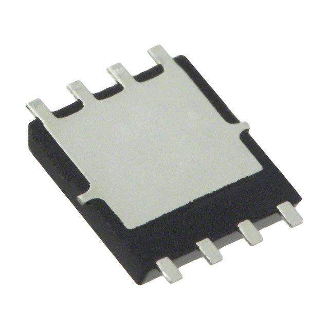
| 产品图片 |
|
| rohs | 符合RoHS无铅 / 符合限制有害物质指令(RoHS)规范要求 |
| 产品系列 | 晶体管,MOSFET,Fairchild Semiconductor FDMS86150PowerTrench® |
| 数据手册 | |
| 产品型号 | FDMS86150 |
| PCN组件/产地 | |
| Pd-PowerDissipation | 156 W |
| Pd-功率耗散 | 156 W |
| RdsOn-Drain-SourceResistance | 4.85 mOhms |
| RdsOn-漏源导通电阻 | 4.85 mOhms |
| Vds-Drain-SourceBreakdownVoltage | 100 V |
| Vds-漏源极击穿电压 | 100 V |
| 不同Id时的Vgs(th)(最大值) | 4V @ 250µA |
| 不同Vds时的输入电容(Ciss) | 4065pF @ 50V |
| 不同Vgs时的栅极电荷(Qg) | 62nC @ 10V |
| 不同 Id、Vgs时的 RdsOn(最大值) | 4.85 毫欧 @ 16A, 10V |
| 产品种类 | MOSFET |
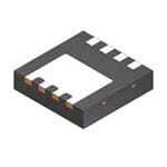
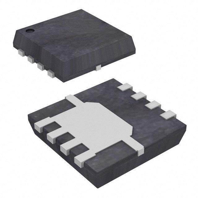
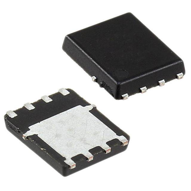
| 供应商器件封装 | Power56 |
| 其它名称 | FDMS86150DKR |
| 功率-最大值 | 2.7W |
| 包装 | Digi-Reel® |
| 单位重量 | 4.376 g |
| 商标 | Fairchild Semiconductor |
| 安装类型 | 表面贴装 |
| 安装风格 | SMD/SMT |
| 封装 | Reel |
| 封装/外壳 | 8-PowerTDFN |
| 封装/箱体 | Power-56-10 |
| 工厂包装数量 | 3000 |
| 晶体管极性 | N-Channel |
| 最大工作温度 | + 150 C |
| 最小工作温度 | - 55 C |
| 标准包装 | 1 |
| 漏源极电压(Vdss) | 100V |
| 特色产品 | http://www.digikey.cn/product-highlights/cn/zh/fairchild-cloud-systems-computing/4301 |
| 电流-连续漏极(Id)(25°C时) | 16A (Ta), 60A (Tc) |
| 系列 | FDMS86150 |


- 商务部:美国ITC正式对集成电路等产品启动337调查
- 曝三星4nm工艺存在良率问题 高通将骁龙8 Gen1或转产台积电
- 太阳诱电将投资9.5亿元在常州建新厂生产MLCC 预计2023年完工
- 英特尔发布欧洲新工厂建设计划 深化IDM 2.0 战略
- 台积电先进制程称霸业界 有大客户加持明年业绩稳了
- 达到5530亿美元!SIA预计今年全球半导体销售额将创下新高
- 英特尔拟将自动驾驶子公司Mobileye上市 估值或超500亿美元
- 三星加码芯片和SET,合并消费电子和移动部门,撤换高东真等 CEO
- 三星电子宣布重大人事变动 还合并消费电子和移动部门
- 海关总署:前11个月进口集成电路产品价值2.52万亿元 增长14.8%


PDF Datasheet 数据手册内容提取
Is Now Part of To learn more about ON Semiconductor, please visit our website at www.onsemi.com Please note: As part of the Fairchild Semiconductor integration, some of the Fairchild orderable part numbers will need to change in order to meet ON Semiconductor’s system requirements. Since the ON Semiconductor product management systems do not have the ability to manage part nomenclature that utilizes an underscore (_), the underscore (_) in the Fairchild part numbers will be changed to a dash (-). This document may contain device numbers with an underscore (_). Please check the ON Semiconductor website to verify the updated device numbers. The most current and up-to-date ordering information can be found at www.onsemi.com. Please email any questions regarding the system integration to Fairchild_questions@onsemi.com. ON Semiconductor and the ON Semiconductor logo are trademarks of Semiconductor Components Industries, LLC dba ON Semiconductor or its subsidiaries in the United States and/or other countries. ON Semiconductor owns the rights to a number of patents, trademarks, copyrights, trade secrets, and other intellectual property. A listing of ON Semiconductor’s product/patent coverage may be accessed at www.onsemi.com/site/pdf/Patent-Marking.pdf. ON Semiconductor reserves the right to make changes without further notice to any products herein. ON Semiconductor makes no warranty, representation or guarantee regarding the suitability of its products for any particular purpose, nor does ON Semiconductor assume any liability arising out of the application or use of any product or circuit, and specifically disclaims any and all liability, including without limitation special, consequential or incidental damages. Buyer is responsible for its products and applications using ON Semiconductor products, including compliance with all laws, regulations and safety requirements or standards, regardless of any support or applications information provided by ON Semiconductor. “Typical” parameters which may be provided in ON Semiconductor data sheets and/or specifications can and do vary in different applications and actual performance may vary over time. All operating parameters, including “Typicals” must be validated for each customer application by customer’s technical experts. ON Semiconductor does not convey any license under its patent rights nor the rights of others. ON Semiconductor products are not designed, intended, or authorized for use as a critical component in life support systems or any FDA Class 3 medical devices or medical devices with a same or similar classification in a foreign jurisdiction or any devices intended for implantation in the human body. Should Buyer purchase or use ON Semiconductor products for any such unintended or unauthorized application, Buyer shall indemnify and hold ON Semiconductor and its officers, employees, subsidiaries, affiliates, and distributors harmless against all claims, costs, damages, and expenses, and reasonable attorney fees arising out of, directly or indirectly, any claim of personal injury or death associated with such unintended or unauthorized use, even if such claim alleges that ON Semiconductor was negligent regarding the design or manufacture of the part. ON Semiconductor is an Equal Opportunity/Affirmative Action Employer. This literature is subject to all applicable copyright laws and is not for resale in any manner.
F D M S 8 March 2015 6 1 FDMS86150 5 0 N-Channel Shielded Gate PowerTrench® MOSFET N - C 100 V, 80 A, 4.85 mΩ h a Features General Description n n e (cid:132) Shielded Gate MOSFET Technology TSheims icoNn-dCuhcatonrn‘se l aMdOvaSnFcEeTd iPs owperroTdruecnecdh ® uspinrogc esFsa ircthhialdt l S (cid:132) Max rDS(on) = 4.85 mΩ at VGS = 10 V, ID = 16 A incorporates Shielded Gate technology. This process has been h i optimized for the on-state resistance and yet maintain superior e (cid:132) Max rDS(on) = 7.8 mΩ at VGS = 6 V, ID = 13 A switching performance. ld (cid:132) Advanced Package and Silicon combination for low r e DS(on) d and high efficiency Applications G (cid:132) MSL1 robust package design a (cid:132) Primary DC-DC MOSFET t e (cid:132) 100% UIL tested (cid:132) Secondary Synchronous Rectifier P (cid:132) RoHS Compliant o (cid:132) Load Switch w e r T r e n c Top Bottom h ® Pin 1 S S D Pin 1 S M S O G S D S F E S D T D D D D G D Power 56 MOSFET Maximum Ratings TA = 25 °C unless otherwise noted Symbol Parameter Ratings Units V Drain to Source Voltage 100 V DS V Gate to Source Voltage ±20 V GS Drain Current -Continuous T = 25 °C 80 C I -Continuous T = 25 °C (Note 1a) 16 A D A -Pulsed 300 E Single Pulse Avalanche Energy (Note 3) 726 mJ AS Power Dissipation T = 25 °C 156 P C W D Power Dissipation T = 25 °C (Note 1a) 2.7 A T , T Operating and Storage Junction Temperature Range -55 to +150 °C J STG Thermal Characteristics R Thermal Resistance, Junction to Case 0.8 θJC °C/W R Thermal Resistance, Junction to Ambient (Note 1a) 45 θJA Package Marking and Ordering Information Device Marking Device Package Reel Size Tape Width Quantity FDMS86150 FDMS86150 Power 56 13 ’’ 12 mm 3000 units ©2012 Fairchild Semiconductor Corporation 1 www.fairchildsemi.com FDMS86150 Rev.1.5
F D Electrical Characteristics T = 25 °C unless otherwise noted M J S Symbol Parameter Test Conditions Min Typ Max Units 8 6 1 Off Characteristics 5 0 BVDSS Drain to Source Breakdown Voltage ID = 250 μA, VGS = 0 V 100 V N Δ BΔVTDSS BCroeeaffkicdioewntn Voltage Temperature ID = 250 μA, referenced to 25 °C 72 mV/°C -C J h I Zero Gate Voltage Drain Current V = 80 V, V = 0 V 1 μA a DSS DS GS n IGSS Gate to Source Leakage Current VGS = ±20 V, VDS = 0 V ±100 nA n e l On Characteristics S h V Gate to Source Threshold Voltage V = V , I = 250 μA 2 3 4 V GS(th) GS DS D i e ΔVGS(th) Gate to Source Threshold Voltage I = 250 μA, referenced to 25 °C -10 mV/°C ld ΔTJ Temperature Coefficient D e d V = 10 V, I = 16 A 3.9 4.85 GS D G r Static Drain to Source On Resistance V = 6 V, I = 13 A 6 7.8 mΩ DS(on) GS D a V = 10 V, I = 16 A, T = 125 °C 7.3 9.1 t GS D J e gFS Forward Transconductance VDS = 10 V, ID = 16 A 53 S P o Dynamic Characteristics w e C Input Capacitance 3055 4065 pF r iss T V = 50 V, V = 0 V, C Output Capacitance DS GS 696 930 pF r oss f = 1 MHz e C Reverse Transfer Capacitance 29 50 pF n rss c R Gate Resistance 0.1 0.7 3.6 Ω h g ® Switching Characteristics M O t Turn-On Delay Time 18 33 ns d(on) S tr Rise Time VDD = 50 V, ID = 16 A, 8.3 17 ns F E td(off) Turn-Off Delay Time VGS = 10 V, RGEN = 6 Ω 28 45 ns T t Fall Time 6 12 ns f Q Total Gate Charge V = 0 V to 10 V 44 62 nC g GS Qg Total Gate Charge VGS = 0 V to 5 V VDD = 50 V, 25 35 nC Qgs Gate to Source Charge ID = 16 A 12.9 nC Q Gate to Drain “Miller” Charge 9.2 nC gd Drain-Source Diode Characteristics V = 0 V, I = 2.1 A (Note 2) 0.69 1.2 V Source to Drain Diode Forward Voltage GS S V SD V = 0 V, I = 16 A (Note 2) 0.78 1.3 GS S t Reverse Recovery Time 69 110 ns rr I = 16 A, di/dt = 100 A/μs Q Reverse Recovery Charge F 94 150 nC rr Notes: 1. RθJA is determined with the device mounted on a 1 in2 pad 2 oz copper pad on a 1.5 x 1.5 in. board of FR-4 material. RθJC is guaranteed by design while RθCA is determined by the user's board design. a. 45 °C/W when mounted on a b. 115 °C/W when mounted on a 1 in2 pad of 2 oz copper. minimum pad of 2 oz copper. GDFDSSFSS GDFDSSFSS 2. Pulse Test: Pulse Width < 300 μs, Duty cycle < 2.0%. 3. EAS of 726 mJ is based on starting TJ = 25 °C, L = 3 mH, IAS = 22 A, VDD = 100 V, VGS = 10 V, 100% test at L = 0.1 mH, IAS = 69 A. ©2012 Fairchild Semiconductor Corporation 2 www.fairchildsemi.com FDMS86150 Rev.1.5
F D Typical Characteristics M T = 25 °C unless otherwise noted J S 8 6 1 300 4 5 VGS = 10 V E 0 250 VGS = 8 V VGS = 7 V NC VGS = 5 V N A A) ST 3 -C NT ( 200 DRESI VGS = 6 V ha AIN CURRE 110500 VGS = 6 V NORMALIZEOURCE ON- 2 VGS = 7 V nnel S I, DRD 50 PDUULTSYE C DYUCRLEA T=I O0.N5 %= 8M0A μXs VGS = 5 V RAIN TO S 1 PDUULTSYE C DYUCRLEA T=I O0.N5 %= 8M0A μXs VGS = 8 V VGS = 10 V hielde 0 D 0 d 0 1 2 3 4 5 0 50 100 150 200 250 300 G VDS, DRAIN TO SO URCE VOLTAGE (V) ID, DRAIN CURR ENT (A) a t e Figure 1. On Region Characteristics Figure 2. Normalized On-Resistance P vs Drain Current and Gate Voltage o w e r T 2.2 20 r e ANCE 2.0 IVDG =S 1=6 1 A0 V )mΩ ID = 16 A PDUULTSYE C DYUCRLEA T=I O0.N5 %= 8M0A μXs nc NORMALIZED O SOURCE ON-RESIST 11111.....02468 rDRAIN TO ,DS(on)(RCE ON-RESISTANCE 11505 TJ = 125 oC hMOSFET® T U AIN 0.8 SO TJ = 25 oC R D 0.6 0 -75 -50 -25 0 25 50 75 100 125 150 4 5 6 7 8 9 10 TJ, JUNCTION TEM PERATURE (oC) VGS, GATE TO SOURCE VOLTAGE (V) Figure 3. Normalized On Resistance Figure 4. On-Resistance vs Gate to vs Junction Temperature Source Voltage 300 300 PULSE DURATION = 80 μs A) 100 VGS = 0 V 250 DUTY CYCLE = 0.5% MAX T ( N T (A)200 VDS = 5 V URRE 10 TJ = 150 oC N C RRE150 AIN 1 TJ = 25 oC U R C D AIN 100 RSE 0.1 I, DRD 50 TJ = 150 oC TJ =T J- 5=5 2 o5C oC I, REVES0.01 TJ = -55 oC 0 0.001 2 3 4 5 6 7 8 0.0 0.2 0.4 0.6 0.8 1.0 1.2 VGS, GATE TO SOU RCE VOLTAGE (V) VSD, BODY DIODE FOR WARD VOLTAGE (V) Figure 5. Transfer Characteristics Figure 6. Source to Drain Diode Forward Voltage vs Source Current ©2012 Fairchild Semiconductor Corporation 3 www.fairchildsemi.com FDMS86150 Rev.1.5
F D Typical Characteristics T = 25 °C unless otherwise noted M J S 8 6 1 10 10000 5 E (V) ID = 16 A VDD = 50 V 0 N OLTAG 8 VDD = 25 V VDD = 75 V pF)1000 Ciss -Ch O SOURCE V 46 PACITANCE ( 100 Coss annel S ATE T 2 CA Crss hie G f = 1 MHz l , GS VGS = 0 V de V 0 10 d 0 10 20 30 40 50 0.1 1 10 100 G Qg, GATE CH ARGE (nC) VDS, DRAIN TO SOU RCE VOLTAGE (V) a t e Figure 7. Gate Charge Characteristics Figure 8. Capacitance vs Drain P to Source Voltage o w e r 100 125 T r e URRENT (A) 10 TJ = 25 oTCJ = 100 oC RRENT (A) 10750 VGS = 10 V nchM® HE C N CU Limited by Package OS AVALANC 1 TJ = 125 oC , IDRAID 2550 VGS = 6 V FET I, AS RθJC = 0.8 oC/W 0.1 0 0.01 0.1 1 10 100 1000 10000100000 25 50 75 100 125 150 tAV, TIME IN AVA LANCHE (ms) TC, CASE TEMPERATURE (oC) Figure 9. Unclamped Inductive Figure 10. Maximum Continuous Drain Switching Capability Current vs Case Temperature 300 1000 V = 10 V 100 W) GS R ( NT (A) 10 POWE 100 AIN CURRE 1 TLIHMISIT AERDE BAY I SrD S(on) 11 0m mss RANSIENT 10 R T D SINGLE PULSE 100 ms K I, D00.0.11 RTTJAθ J ==A M2=5 A1 Xo1C 5R oACT/WED 1D10 Cs s , PPEA()PK 0.15 TSRAIθNJ =AG 2=L5 E1 o 1PC5U oLCS/WE 0.01 0.1 1 10 100 500 10-3 10-2 10-1 1 10 100 1000 VDS, DRAIN to SOU RCE VOLTAGE (V) t, PULSE WI DTH (sec) Figure 11. Forward Bias Safe Figure 12. Single Pulse Maximum Operating Area Power Dissipation ©2012 Fairchild Semiconductor Corporation 4 www.fairchildsemi.com FDMS86150 Rev.1.5
F D Typical Characteristics T = 25 °C unless otherwise noted M J S 8 2 6 SIENT 1 DUTY CYCLE-DESCENDING ORDER 150 AN D = 0.5 N EFFECTIVE TRL RESISTANCE 0.1 00000.....21000521 PDM t1 -Channe LIZED ERMA 0.01 NOTES: t2 l Sh NORMATH SINGLE PULSE RZPθθeJJaAAk( =t T) 1J=1 =r5( Pt°)CD xM/ WR xθ JZAθJA(t) + TA ield r(t), 0.00110-3 10-2 10-1 1 10 Duty C1yc0l0e, D = t1 / t2 1000 ed G t, RECTANGULAR PULSE DURATION (sec) a t e Figure 13. Junction-to-Ambient Transient Thermal Response Curve P o w e r T r e n c h ® M O S F E T ©2012 Fairchild Semiconductor Corporation 5 www.fairchildsemi.com FDMS86150 Rev.1.5
5.10 A 4.90 4.42 PKG 3.81 CL B 8 5 8 7 6 5 1.14 KEEP OUT AREA 3.65 PKG CL 6.25 5.90 4.79 6.61 1.27 PIN #1 1 4 IDICATOR TOP VIEW 1 2 3 4 1.27 0.61 SEE DETAIL A 3.81 5.10 LAND PATTERN SIDE VIEW RECOMMENDATION 3.81 0.10 C A B 1.27 0.47 (0.38) (8X) 0.37 1 4 (0.35) 0.65 0.55 NOTES: UNLESS OTHERWISE SPECIFIED A) PACKAGE STANDARD REFERENCE: JEDEC MO-240, ISSUE A, VAR. AA, PIN #1 B) ALL DIMENSIONS ARE IN MILLIMETERS. INDICATOR 4.66 4.46 C) DIMENSIONS DO NOT INCLUDE BURRS OR MOLD FLASH. MOLD FLASH OR BURRS DOES NOT EXCEED 0.10MM. D) DIMENSIONING AND TOLERANCING PER 8 5 ASME Y14.5M-2009. 0.70 E) IT IS RECOMMENDED TO HAVE NO TRACES 4.33 4.13 OR VIAS WITHIN THE KEEP OUT AREA. F) DRAWING FILE NAME: PQFN08JREV3. BOTTOM VIEW 0.10 C 1.10 0.90 0.08 C C 0.25 0.05 0.15 0.00 SEATING PLANE SCALE: 2:1
ON Semiconductor and are trademarks of Semiconductor Components Industries, LLC dba ON Semiconductor or its subsidiaries in the United States and/or other countries. ON Semiconductor owns the rights to a number of patents, trademarks, copyrights, trade secrets, and other intellectual property. A listing of ON Semiconductor’s product/patent coverage may be accessed at www.onsemi.com/site/pdf/Patent−Marking.pdf. ON Semiconductor reserves the right to make changes without further notice to any products herein. ON Semiconductor makes no warranty, representation or guarantee regarding the suitability of its products for any particular purpose, nor does ON Semiconductor assume any liability arising out of the application or use of any product or circuit, and specifically disclaims any and all liability, including without limitation special, consequential or incidental damages. Buyer is responsible for its products and applications using ON Semiconductor products, including compliance with all laws, regulations and safety requirements or standards, regardless of any support or applications information provided by ON Semiconductor. “Typical” parameters which may be provided in ON Semiconductor data sheets and/or specifications can and do vary in different applications and actual performance may vary over time. All operating parameters, including “Typicals” must be validated for each customer application by customer’s technical experts. ON Semiconductor does not convey any license under its patent rights nor the rights of others. ON Semiconductor products are not designed, intended, or authorized for use as a critical component in life support systems or any FDA Class 3 medical devices or medical devices with a same or similar classification in a foreign jurisdiction or any devices intended for implantation in the human body. Should Buyer purchase or use ON Semiconductor products for any such unintended or unauthorized application, Buyer shall indemnify and hold ON Semiconductor and its officers, employees, subsidiaries, affiliates, and distributors harmless against all claims, costs, damages, and expenses, and reasonable attorney fees arising out of, directly or indirectly, any claim of personal injury or death associated with such unintended or unauthorized use, even if such claim alleges that ON Semiconductor was negligent regarding the design or manufacture of the part. ON Semiconductor is an Equal Opportunity/Affirmative Action Employer. This literature is subject to all applicable copyright laws and is not for resale in any manner. PUBLICATION ORDERING INFORMATION LITERATURE FULFILLMENT: N. American Technical Support: 800−282−9855 Toll Free ON Semiconductor Website: www.onsemi.com Literature Distribution Center for ON Semiconductor USA/Canada 19521 E. 32nd Pkwy, Aurora, Colorado 80011 USA Europe, Middle East and Africa Technical Support: Order Literature: http://www.onsemi.com/orderlit Phone: 303−675−2175 or 800−344−3860 Toll Free USA/Canada Phone: 421 33 790 2910 Fax: 303−675−2176 or 800−344−3867 Toll Free USA/Canada Japan Customer Focus Center For additional information, please contact your local Email: orderlit@onsemi.com Phone: 81−3−5817−1050 Sales Representative © Semiconductor Components Industries, LLC www.onsemi.com www.onsemi.com 1
Mouser Electronics Authorized Distributor Click to View Pricing, Inventory, Delivery & Lifecycle Information: O N Semiconductor: FDMS86150