ICGOO在线商城 > 分立半导体产品 > 晶体管 - FET,MOSFET - 射频 > BF1202R,215
 Datasheet下载
- 型号: BF1202R,215
- 制造商: NXP Semiconductors
- 库位|库存: xxxx|xxxx
- 要求:
| 数量阶梯 | 香港交货 | 国内含税 |
| +xxxx | $xxxx | ¥xxxx |
查看当月历史价格
查看今年历史价格
BF1202R,215产品简介:
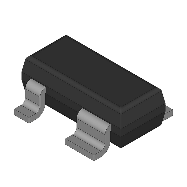
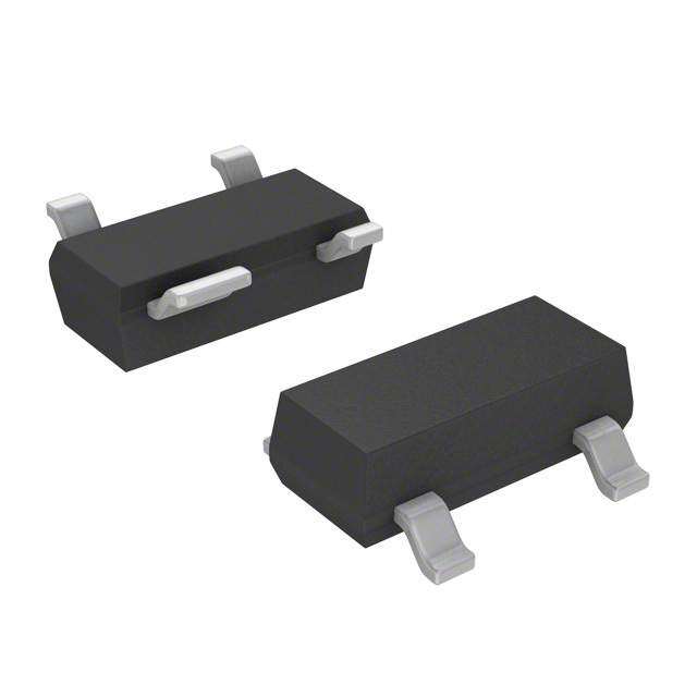
ICGOO电子元器件商城为您提供BF1202R,215由NXP Semiconductors设计生产,在icgoo商城现货销售,并且可以通过原厂、代理商等渠道进行代购。 BF1202R,215价格参考¥2.00-¥2.00。NXP SemiconductorsBF1202R,215封装/规格:晶体管 - FET,MOSFET - 射频, 射频 Mosfet N 通道双门 5V 12mA 400MHz 30.5dB 200mW SOT-143R。您可以下载BF1202R,215参考资料、Datasheet数据手册功能说明书,资料中有BF1202R,215 详细功能的应用电路图电压和使用方法及教程。
BF1202R,215 是 NXP USA Inc. 生产的一款射频 MOSFET 晶体管,适用于高频、低功率射频应用。该器件常用于无线通信系统中的射频信号放大、调制与混频等电路。典型应用场景包括:

1. 无线通信设备:如蜂窝基站、Wi-Fi接入点、射频收发模块等,用于射频信号的低噪声放大或功率放大;
2. 广播设备:在FM广播、电视发射系统中作为射频放大器;
3. 工业控制与测量仪器:用于射频识别(RFID)、测试仪器中的射频信号处理;
4. 消费类电子产品:如高端路由器、射频遥控装置等;
5. 军事与航空航天领域:在雷达、导航系统中进行射频信号增强。

该器件具有良好的高频特性与稳定性,适合在UHF频段及以下频率使用。由于其215后缀为标准Tape & Reel封装形式,便于自动化贴片生产。
| 参数 | 数值 |
| 产品目录 | |
| 描述 | MOSFET 2N-CH 10V 30MA SOT143R |
| 产品分类 | RF FET |
| 品牌 | NXP Semiconductors |
| 数据手册 | |
| 产品图片 |
|
| 产品型号 | BF1202R,215 |
| PCN封装 | |
| PCN过时产品 | |
| rohs | 无铅 / 符合限制有害物质指令(RoHS)规范要求 |
| 产品系列 | - |
| 供应商器件封装 | SOT-143R |
| 其它名称 | 568-6152-6 |
| 功率-输出 | 200mW |
| 包装 | 带卷 (TR) |
| 噪声系数 | 0.9dB |
| 增益 | 30.5dB |
| 封装/外壳 | TO-253-4,TO-253AA |
| 晶体管类型 | N 通道双门 |
| 标准包装 | 1 |
| 电压-测试 | 5V |
| 电压-额定 | 10V |
| 电流-测试 | 12mA |
| 频率 | 400MHz |
| 额定电流 | 30mA |


- 商务部:美国ITC正式对集成电路等产品启动337调查
- 曝三星4nm工艺存在良率问题 高通将骁龙8 Gen1或转产台积电
- 太阳诱电将投资9.5亿元在常州建新厂生产MLCC 预计2023年完工
- 英特尔发布欧洲新工厂建设计划 深化IDM 2.0 战略
- 台积电先进制程称霸业界 有大客户加持明年业绩稳了
- 达到5530亿美元!SIA预计今年全球半导体销售额将创下新高
- 英特尔拟将自动驾驶子公司Mobileye上市 估值或超500亿美元
- 三星加码芯片和SET,合并消费电子和移动部门,撤换高东真等 CEO
- 三星电子宣布重大人事变动 还合并消费电子和移动部门
- 海关总署:前11个月进口集成电路产品价值2.52万亿元 增长14.8%

PDF Datasheet 数据手册内容提取
DISCRETE SEMICONDUCTORS DATA SHEET BF1202; BF1202R; BF1202WR N-channel dual-gate PoLo MOS-FETs Product specification 2010 Sep 16 Supersedes data of 2000 Mar 29
NXP Semiconductors Product specification N-channel dual-gate PoLo MOS-FETs BF1202; BF1202R; BF1202WR FEATURES PINNING Short channel transistor with high PIN DESCRIPTION handbook, 2 co3lumns 4 forward transfer admittance to input 1 source capacitance ratio 2 drain Low noise gain controlled amplifier 3 gate2 Partly internal self-biasing circuit to 2 1 4 gate1 ensure good cross-modulation performance during AGC and good Top view MSB035 DCstabilization. Marking code legend: BF1202R marking code: LE* * = - : made in Hong Kong APPLICATIONS * = p : made in Hong Kong Fig.2 Simplified outline VHF and UHF applications with * = t : made in Malaysia (SOT143R). 3to9V supply voltage, such as digital and analogue television tuners and professional communications equipment. handbook, 2 c4olumns 3 lfpage 3 4 DESCRIPTION Enhancement type N-channel field-effect transistor with source and 1 2 substrate interconnected. Integrated 2 1 diodes between gates and source Top view MSB014 Top view MSB842 protect against excessive input voltage surges. The BF1202, BF1202 marking code: LD* BF1202WR marking code: LE* BF1202R and BF1202WR are encapsulated in the SOT143B, Fig.1 Simplified outline Fig.3 Simplified outline SOT143R and SOT343R plastic (SOT143B). (SOT343R). packages respectively. QUICK REFERENCE DATA SYMBOL PARAMETER CONDITIONS MIN. TYP. MAX. UNIT V drain-source voltage 10 V DS I drain current 30 mA D P total power dissipation 200 mW tot y forward transfer admittance 25 30 40 mS fs C input capacitance at gate1 1.7 2.2 pF ig1-ss C reverse transfer capacitance f=1MHz 15 30 fF rss F noise figure f=800MHz 1.1 1.8 dB X cross-modulation input level for k=1% at 100 105 dBV mod 40dB AGC T operating junction temperature 150 C j CAUTION This product is supplied in anti-static packing to prevent damage caused by electrostatic discharge during transport and handling. 2010 Sep 16 2
NXP Semiconductors Product specification N-channel dual-gate PoLo MOS-FETs BF1202; BF1202R; BF1202WR LIMITING VALUES In accordance with the Absolute Maximum Rating System (IEC60134). SYMBOL PARAMETER CONDITIONS MIN. MAX. UNIT V drain-source voltage 10 V DS I drain current 30 mA D I gate1 current 10 mA G1 I gate2 current 10 mA G2 P total power dissipation tot BF1202; BF1202R T 113C; note1 200 mW s BF1202WR T 119C; note1 200 mW s T storage temperature 65 +150 C stg T operating junction temperature 150 C j Note 1. T is the temperature of the soldering point of the source lead. s THERMAL CHARACTERISTICS SYMBOL PARAMETER VALUE UNIT R thermal resistance from junction to soldering point th j-s BF1202; BF1202R 185 K/W BF1202WR 155 K/W MCD951 250 handbook, halfpage Ptot (mW) 200 (2) (1) 150 100 50 0 0 50 100 150 200 Ts (°C) (1) BF1202WR. (2) BF1202; BF1202R. Fig.4 Power derating curve. 2010 Sep 16 3
NXP Semiconductors Product specification N-channel dual-gate PoLo MOS-FETs BF1202; BF1202R; BF1202WR STATIC CHARACTERISTICS T =25C unless otherwise specified. j SYMBOL PARAMETER CONDITIONS MIN. MAX. UNIT V drain-source breakdown voltage V =V =0; I =10A 10 V (BR)DSS G1-S G2-S D V gate1-source breakdown voltage V =V =0; I =10mA 6 V (BR)G1-SS G2-S DS G1-S V gate2-source breakdown voltage V =V =0; I =10mA 6 V (BR)G2-SS G1-S DS G2-S V forward source-gate1 voltage V =V =0; I =10mA 0.5 1.5 V (F)S-G1 G2-S DS S-G1 V forward source-gate2 voltage V =V =0; I =10mA 0.5 1.5 V (F)S-G2 G1-S DS S-G2 V gate1-source threshold voltage V =4V; V =5V; I =100A 0.3 1.0 V G1-S(th) G2-S DS D V gate2-source threshold voltage V =5V; V =5V; I =100A 0.3 1.2 V G2-S(th) G1-S DS D I drain-source current V =4V; V =5V; R =120k; 8 16 mA DSX G2-S DS G1 note1 I gate1 cut-off current V =V =0; V =5V 50 nA G1-SS G2-S DS G1-S I gate2 cut-off current V =V =0; V =4V 20 nA G2-SS G1-S DS G2-S Note 1. R connects G toV =5V. G1 1 GG DYNAMIC CHARACTERISTICS Common source; T =25C; V =4V; V =5V; I =12mA; unless otherwise specified. amb G2-S DS D SYMBOL PARAMETER CONDITIONS MIN. TYP. MAX. UNIT y forward transfer admittance pulsed; T =25C 25 30 40 mS fs j C input capacitance at gate1 f=1MHz 1.7 2.2 pF ig1-ss C input capacitance at gate2 f=1MHz 1 pF ig2-ss C output capacitance f=1MHz 0.85 pF oss C reverse transfer capacitance f=1MHz 15 30 fF rss F noise figure f=10.7MHz; G =20mS; B =0 9 11 dB S S f=400MHz; Y =Y 0.9 1.5 dB S Sopt f=800MHz; Y =Y 1.1 1.8 dB S Sopt G power gain f=200MHz; G =2mS; B =B ; 34.5 dB tr S S Sopt G =0.5mS; B =B L L Lopt f=400MHz; G =2mS; B =B ; 30.5 dB S S Sopt G =1mS; B =B L L Lopt f=800MHz; G =3.3mS; B =B ; 26.5 dB S S Sopt G =1mS; B =B L L Lopt X cross-modulation input level for k=1%; f =50MHz; mod w f =60MHz; note1 unw at 0dB AGC 90 dB V at 10dB AGC 92 dBV at 40dB AGC 100 105 dBV Note 1. Measured in Fig.21 test circuit. 2010 Sep 16 4
NXP Semiconductors Product specification N-channel dual-gate PoLo MOS-FETs BF1202; BF1202R; BF1202WR MCD952 MCD953 20 24 handbooIkD, halfpage VG2-S = 4 V 2.5 V handbook, halfpage (mA) 3.5 V ID VG1-S = 1.5 V 16 2 V (mA) 3 V 1.4 V 16 12 1.3 V 1.5 V 1.2 V 8 8 1.1 V 1 V 4 1 V 0.9 V 0 0 0 0.4 0.8 1.2 1.6 2 0 2 4 6 8 10 VG1-S (V) VDS (V) VDS=5V. VG2-S=4V. Tj=25C. Tj=25C. Fig.5 Transfer characteristics; typical values. Fig.6 Output characteristics; typical values. MCD954 MCD955 100 40 handbooIGk, 1halfpage VG2-S = 4 V 3.5 V handbook, halfpage 3.5 V (μA) 3 V yfs 80 (mS) VG2-S = 4 V 30 3 V 60 2.5 V 20 2.5 V 40 2 V 10 20 1.5 V 2 V 1 V 0 0 0 0.5 1 1.5 2 2.5 0 4 8 12 16 20 VG1-S (V) ID (mA) VVDDSS==55VV.. VDS=5V. TTjj==2255CC.. Tj=25C. Fig.7 Gate1 current as a function of gate1 Fig.8 Forward transfer admittance as a function voltage; typical values. of drain current; typical values. 2010 Sep 16 5
NXP Semiconductors Product specification N-channel dual-gate PoLo MOS-FETs BF1202; BF1202R; BF1202WR handbooIkD,2 h0alfpage MCD956 handbook,1 h6alfpage MCD957 (mA) ID (mA) 16 12 12 8 8 4 4 0 0 0 10 20 30 40 50 0 1 2 3 4 5 IG1 (μA) VGG (V) VDS=5V; VG2-S=4V. VDS=5V; VG2-S=4V; Tj=25C. Tj=25C. RG1=120k (connected to VGG); seeFig.21. Fig.9 Drain current as a function of gate1 current; Fig.10 Drain current as a function of gate1 supply typical values. voltage (=V ); typical values. GG handbo(omIkD,A2 h0)alfpage RG1 = 6M8C kDΩ958 handbo(omkID,1A h6)alfpage VGG = 5M VCD959 16 82 kΩ 4.5 V 12 100 kΩ 4 V 120 kΩ 3.5 V 12 150 kΩ 3 V 8 180 kΩ 8 220 kΩ 4 4 0 0 0 2 4 6 0 2 4 6 VGG = VDS (V) VG2-S (V) VG2-S=4V; Tj=25C. VDS=5V; Tj=25C. RG1 connected to VGG; seeFig.21. RG1=120k (connected to VGG); see Fig.21. Fig.11 Drain current as a function of gate1 (=V ) Fig.12 Drain current as a function of gate2 GG and drain supply voltage; typical values. voltage; typical values. 2010 Sep 16 6
NXP Semiconductors Product specification N-channel dual-gate PoLo MOS-FETs BF1202; BF1202R; BF1202WR MCD960 MCD961 40 0 handbook, halfpage handgbaoionk, halfpage IG1 reduction (μA) VGG = 5 V (dB)−10 30 4.5 V 4 V −20 20 3.5 V 3 V −30 10 −40 0 −50 0 2 4 6 0 1 2 3 4 VG2-S (V) VAGC (V) VDS=5V; Tj=25C. VDS=5V; VGG=5V; RG1=120k; RG1=120k (connected to VGG); see Fig.21. f=50MHz; Tamb=25C. Fig.13 Gate1 current as a function of gate2 Fig.14 Typical gain reduction as a function of the voltage; typical values. AGC voltage; see Fig.21. MCD962 handboo1k,2 h0alfpage 16 MCD963 Vunw handbook, halfpage (dBμV) ID (mA) 110 12 100 8 90 4 80 0 10 20 30 40 50 0 gain reduction (dB) 0 10 20 30 40 50 gain reduction (dB) VDS=5V; VGG=5V; RG1=120k; f=50MHz; funw=60MHz; Tamb=25C. VDS=5V; VGG=5V; RG1=120k; f=50MHz; Tamb=25C. Fig.15 Unwanted voltage for1% cross-modulation as a function of gain reduction; typical Fig.16 Drain current as a function of gain values; Fig.21. reduction; typical values; see Fig.21. 2010 Sep 16 7
NXP Semiconductors Product specification N-channel dual-gate PoLo MOS-FETs BF1202; BF1202R; BF1202WR handbook1, 0h2alfpage MCD964 103 MCD965 −103 handbook, halfpage Yis yrs ϕrs (mS) (μS) (deg) ϕ 10 102 rs −102 bis gis yrs 1 10 −10 10−110 102 103 1 −1 f (GHz) 10 102 103 f (MHz) VDS=5V; VG2=4V. VDS=5V; VG2=4V. ID=12mA; Tamb=25C. ID=12mA; Tamb=25C. Fig.17 Input admittance as a function of frequency; Fig.18 Reverse transfer admittance and phase as typical values. a function of frequency; typical values. 102 MCD966 −102 10 MCD967 handbook, halfpage handbook, halfpage yfs ϕfs Yos (mS) (deg) (mS) yfs bos 1 10 −10 ϕ fs 10−1 gos 1 −1 10−2 10 102 103 10 102 103 f (MHz) f (MHz) VDS=5V; VG2=4V. VDS=5V; VG2=4V. ID=12mA; Tamb=25C. ID=12mA; Tamb=25C. Fig.19 Forward transfer admittance and phase as Fig.20 Output admittance as a function of a function of frequency; typical values. frequency; typical values. 2010 Sep 16 8
NXP Semiconductors Product specification N-channel dual-gate PoLo MOS-FETs BF1202; BF1202R; BF1202WR handbook, full pagewidth VAGC R1 10 kΩ C1 4.7 nF C3 4.7 nF C2 DUT L≈12.2 μH R50L Ω RGEN R2 4.7 nF C4 50 Ω 50 Ω RG1 4.7 nF VI VGG VDS MGS315 Fig.21 Cross-modulation test set-up. Table 1 Scattering parameters: V =5V; V =4V; I =12mA; T =25C DS G2-S D amb s s s s 11 21 12 22 f (MHz) MAGNITUDE ANGLE MAGNITUDE ANGLE MAGNITUDE ANGLE MAGNITUDE ANGLE (ratio) (deg) (ratio) (deg) (ratio) (deg) (ratio) (deg) 50 0.988 3.26 2.989 176.2 0.0005 92.6 0.995 1.50 100 0.988 6.52 3.017 172.5 0.0009 88.0 0.995 3.01 200 0.984 12.99 2.990 165.0 0.0018 82.5 0.994 5.95 300 0.977 19.39 2.949 157.6 0.0027 78.2 0.992 8.86 400 0.965 25.65 2.913 150.3 0.0036 75.4 0.990 11.79 500 0.951 31.76 2.853 143.2 0.0039 71.8 0.988 14.65 600 0.936 37.68 2.793 136.3 0.0042 69.9 0.986 17.41 700 0.919 43.42 2.727 129.5 0.0044 68.9 0.984 20.10 800 0.903 48.94 2.664 123.0 0.0043 68.5 0.980 22.69 900 0.887 54.25 2.593 116.7 0.0041 70.7 0.975 25.27 1000 0.870 59.34 2.518 110.5 0.0038 72.4 0.970 27.90 Table 2 Noise data: V =5V; V =4V; I =12mA; T =25C DS G2-S D amb f F opt R min n (MHz) (dB) () (ratio) (deg) 400 0.9 0.805 28.5 50 800 1.1 0.725 47.2 40 2010 Sep 16 9
NXP Semiconductors Product specification N-channel dual-gate PoLo MOS-FETs BF1202; BF1202R; BF1202WR PACKAGE OUTLINES Plastic surface-mounted package; 4 leads SOT143B D B E A X y v M A HE e bp w M B 4 3 Q A A1 c 1 2 Lp b1 e1 detail X 0 1 2 mm scale DIMENSIONS (mm are the original dimensions) UNIT A mAa1x bp b1 c D E e e1 HE Lp Q v w y 1.1 0.48 0.88 0.15 3.0 1.4 2.5 0.45 0.55 mm 0.1 1.9 1.7 0.2 0.1 0.1 0.9 0.38 0.78 0.09 2.8 1.2 2.1 0.15 0.45 OUTLINE REFERENCES EUROPEAN ISSUE DATE VERSION IEC JEDEC JEITA PROJECTION 04-11-16 SOT143B 06-03-16 2010 Sep 16 10
NXP Semiconductors Product specification N-channel dual-gate PoLo MOS-FETs BF1202; BF1202R; BF1202WR Plastic surface-mounted package; reverse pinning; 4 leads SOT143R D B E A X y v M A HE e bp w M B 3 4 Q A A1 c 2 1 Lp b1 e1 detail X 0 1 2 mm scale DIMENSIONS (mm are the original dimensions) UNIT A A1 bp b1 c D E e e1 HE Lp Q v w y max 1.1 0.48 0.88 0.15 3.0 1.4 2.5 0.55 0.45 mm 0.1 1.9 1.7 0.2 0.1 0.1 0.9 0.38 0.78 0.09 2.8 1.2 2.1 0.25 0.25 OUTLINE REFERENCES EUROPEAN ISSUE DATE VERSION IEC JEDEC JEITA PROJECTION 04-11-16 SOT143R SC-61AA 06-03-16 2010 Sep 16 11
NXP Semiconductors Product specification N-channel dual-gate PoLo MOS-FETs BF1202; BF1202R; BF1202WR Plastic surface-mounted package; reverse pinning; 4 leads SOT343R D B E A X y HE v M A e 3 4 Q A A1 c 2 1 w M B bp b1 Lp e1 detail X 0 1 2 mm scale DIMENSIONS (mm are the original dimensions) UNIT A mAa1x bp b1 c D E e e1 HE Lp Q v w y 1.1 0.4 0.7 0.25 2.2 1.35 2.2 0.45 0.23 mm 0.1 1.3 1.15 0.2 0.2 0.1 0.8 0.3 0.5 0.10 1.8 1.15 2.0 0.15 0.13 OUTLINE REFERENCES EUROPEAN ISSUE DATE VERSION IEC JEDEC EIAJ PROJECTION 97-05-21 SOT343R 06-03-16 2010 Sep 16 12
NXP Semiconductors Product specification N-channel dual-gate PoLo MOS-FETs BF1202; BF1202R; BF1202WR DATA SHEET STATUS DOCUMENT PRODUCT DEFINITION STATUS(1) STATUS(2) Objective data sheet Development This document contains data from the objective specification for product development. Preliminary data sheet Qualification This document contains data from the preliminary specification. Product data sheet Production This document contains the product specification. Notes 1. Please consult the most recently issued document before initiating or completing a design. 2. The product status of device(s) described in this document may have changed since this document was published and may differ in case of multiple devices. The latest product status information is available on the Internet at URLhttp://www.nxp.com. DISCLAIMERS property or environmental damage. NXP Semiconductors accepts no liability for inclusion and/or use of NXP Limited warranty and liability Information in this Semiconductors products in such equipment or document is believed to be accurate and reliable. applications and therefore such inclusion and/or use is at However, NXP Semiconductors does not give any the customer’s own risk. representations or warranties, expressed or implied, as to the accuracy or completeness of such information and Applications Applications that are described herein for shall have no liability for the consequences of use of such any of these products are for illustrative purposes only. information. NXP Semiconductors makes no representation or warranty that such applications will be suitable for the In no event shall NXP Semiconductors be liable for any specified use without further testing or modification. indirect, incidental, punitive, special or consequential damages (including - without limitation - lost profits, lost Customers are responsible for the design and operation of savings, business interruption, costs related to the their applications and products using NXP removal or replacement of any products or rework Semiconductors products, and NXP Semiconductors charges) whether or not such damages are based on tort accepts no liability for any assistance with applications or (including negligence), warranty, breach of contract or any customer product design. It is customer’s sole other legal theory. responsibility to determine whether the NXP Semiconductors product is suitable and fit for the Notwithstanding any damages that customer might incur customer’s applications and products planned, as well as for any reason whatsoever, NXP Semiconductors’ for the planned application and use of customer’s third aggregate and cumulative liability towards customer for party customer(s). Customers should provide appropriate the products described herein shall be limited in design and operating safeguards to minimize the risks accordance with the Terms and conditions of commercial associated with their applications and products. sale of NXP Semiconductors. NXP Semiconductors does not accept any liability related Right to make changes NXP Semiconductors to any default, damage, costs or problem which is based reserves the right to make changes to information on any weakness or default in the customer’s applications published in this document, including without limitation or products, or the application or use by customer’s third specifications and product descriptions, at any time and party customer(s). Customer is responsible for doing all without notice. This document supersedes and replaces all necessary testing for the customer’s applications and information supplied prior to the publication hereof. products using NXP Semiconductors products in order to Suitability for use NXP Semiconductors products are avoid a default of the applications and the products or of not designed, authorized or warranted to be suitable for the application or use by customer’s third party use in life support, life-critical or safety-critical systems or customer(s). NXP does not accept any liability in this equipment, nor in applications where failure or malfunction respect. of an NXP Semiconductors product can reasonably be expected to result in personal injury, death or severe 2010 Sep 16 13
NXP Semiconductors Product specification N-channel dual-gate PoLo MOS-FETs BF1202; BF1202R; BF1202WR Limiting values Stress above one or more limiting Quick reference data The Quick reference data is an values (as defined in the Absolute Maximum Ratings extract of the product data given in the Limiting values and System of IEC60134) will cause permanent damage to Characteristics sections of this document, and as such is the device. Limiting values are stress ratings only and not complete, exhaustive or legally binding. (proper) operation of the device at these or any other Non-automotive qualified products Unless this data conditions above those given in the Recommended sheet expressly states that this specific NXP operating conditions section (if present) or the Semiconductors product is automotive qualified, the Characteristics sections of this document is not warranted. product is not suitable for automotive use. It is neither Constant or repeated exposure to limiting values will qualified nor tested in accordance with automotive testing permanently and irreversibly affect the quality and or application requirements. NXP Semiconductors accepts reliability of the device. no liability for inclusion and/or use of non-automotive Terms and conditions of commercial sale NXP qualified products in automotive equipment or Semiconductors products are sold subject to the general applications. terms and conditions of commercial sale, as published at In the event that customer uses the product for design-in http://www.nxp.com/profile/terms, unless otherwise and use in automotive applications to automotive agreed in a valid written individual agreement. In case an specifications and standards, customer (a) shall use the individual agreement is concluded only the terms and product without NXP Semiconductors’ warranty of the conditions of the respective agreement shall apply. NXP product for such automotive applications, use and Semiconductors hereby expressly objects to applying the specifications, and (b) whenever customer uses the customer’s general terms and conditions with regard to the product for automotive applications beyond NXP purchase of NXP Semiconductors products by customer. Semiconductors’ specifications such use shall be solely at No offer to sell or license Nothing in this document customer’s own risk, and (c) customer fully indemnifies may be interpreted or construed as an offer to sell products NXP Semiconductors for any liability, damages or failed that is open for acceptance or the grant, conveyance or product claims resulting from customer design and use of implication of any license under any copyrights, patents or the product for automotive applications beyond NXP other industrial or intellectual property rights. Semiconductors’ standard warranty and NXP Semiconductors’ product specifications. Export control This document as well as the item(s) described herein may be subject to export control regulations. Export might require a prior authorization from national authorities. 2010 Sep 16 14
NXP Semiconductors provides High Performance Mixed Signal and Standard Product solutions that leverage its leading RF, Analog, Power Management, Interface, Security and Digital Processing expertise Customer notification This data sheet was changed to reflect the new company name NXP Semiconductors, including new legal definitions and disclaimers. No changes were made to the technical content, except for the marking codes and the package outline drawings which were updated to the latest version. Contact information For additional information please visit: http://www.nxp.com For sales offices addresses send e-mail to: salesaddresses@nxp.com © NXP B.V. 2010 All rights are reserved. Reproduction in whole or in part is prohibited without the prior written consent of the copyright owner. The information presented in this document does not form part of any quotation or contract, is believed to be accurate and reliable and may be changed without notice. No liability will be accepted by the publisher for any consequence of its use. Publication thereof does not convey nor imply any license under patent- or other industrial or intellectual property rights. Printed in The Netherlands R77/03/pp15 Date of release: 2010 Sep 16