ICGOO在线商城 > 分立半导体产品 > 晶体管 - JFET > 2N5458

 Datasheet下载
- 型号: 2N5458
- 制造商: Central Semiconductor
- 库位|库存: xxxx|xxxx
- 要求:
| 数量阶梯 | 香港交货 | 国内含税 |
| +xxxx | $xxxx | ¥xxxx |
查看当月历史价格
查看今年历史价格
2N5458产品简介:
ICGOO电子元器件商城为您提供2N5458由Central Semiconductor设计生产,在icgoo商城现货销售,并且可以通过原厂、代理商等渠道进行代购。 2N5458价格参考。Central Semiconductor2N5458封装/规格:晶体管 - JFET, JFET N-Channel 25V 310mW Through Hole TO-92-3。您可以下载2N5458参考资料、Datasheet数据手册功能说明书,资料中有2N5458 详细功能的应用电路图电压和使用方法及教程。
2N5458是安森美半导体(ON Semiconductor)生产的一款N沟道结型场效应晶体管(JFET),常用于低噪声、高输入阻抗的模拟电路中。其主要应用场景包括:

1. 音频放大器:由于2N5458具有较低的噪声系数和良好的线性特性,广泛应用于前置音频放大器和高保真音响设备中,作为输入级以提高信号采集的精度与清晰度。

2. 仪表放大器与传感器接口:该器件具备高输入阻抗特性,适合用于精密测量仪器、传感器信号调理电路中,用以放大微弱模拟信号并减少对信号源的影响。

3. 射频(RF)前端电路:在低频至中频的射频接收系统中,2N5458可用于构建低噪声放大器(LNA),有助于提升系统的整体灵敏度。

4. 电压控制电阻应用:JFET可在可变电阻模式下工作,2N5458因此也适用于自动增益控制(AGC)、电子音量调节等场合。

5. 教育与实验用途:因其参数稳定且易于使用,2N5458也常被用于电子工程教学实验中,帮助学生理解FET的工作原理及基本放大电路的设计。

综上,2N5458凭借其低噪声、高输入阻抗和良好稳定性,广泛应用于音频、测量、通信等领域中的模拟信号处理电路。
| 参数 | 数值 |
| Id-ContinuousDrainCurrent | 10 mA |
| Id-连续漏极电流 | 10 mA |
| 品牌 | Central Semiconductor |
| 产品目录 | 半导体 |
| 描述 | JFET N-Ch/AMP |
| 产品分类 | 分离式半导体 |
| 产品手册 | |
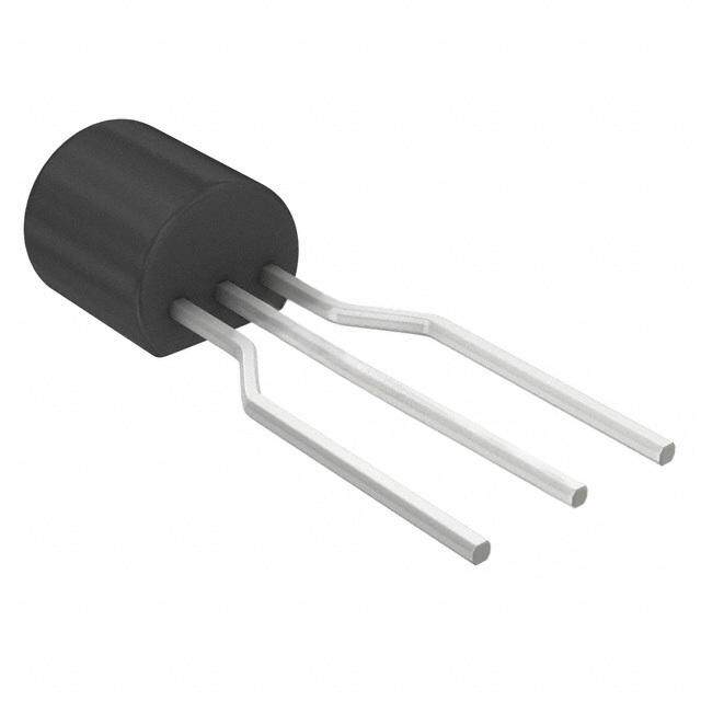
| 产品图片 |
|
| rohs | 过渡期间 |
| 产品系列 | 晶体管,JFET,Central Semiconductor 2N5458 |
| 产品型号 | 2N5458 |
| Pd-PowerDissipation | 310 mW |
| Pd-功率耗散 | 310 mW |
| Vds-Drain-SourceBreakdownVoltage | 25 V |
| Vds-漏源极击穿电压 | 25 V |
| Vgs-Gate-SourceBreakdownVoltage | 25 V |
| Vgs-栅源极击穿电压 | 25 V |
| Vgs=0时的漏-源电流 | 2 mA to 9 mA |
| 产品种类 | JFET |
| 功率耗散 | 310 mW |
| 商标 | Central Semiconductor |
| 安装风格 | Through Hole |
| 封装 | Bulk |
| 封装/箱体 | TO-92 |
| 工厂包装数量 | 2500 |
| 晶体管极性 | N-Channel |
| 正向跨导-最小值 | 0.0015 S to 0.0055 S |
| 漏极连续电流 | 10 mA |
| 漏源电压VDS | 25 V |
| 系列 | 2N5458 |
| 配置 | Single |
| 闸/源击穿电压 | 25 V |


- 商务部:美国ITC正式对集成电路等产品启动337调查
- 曝三星4nm工艺存在良率问题 高通将骁龙8 Gen1或转产台积电
- 太阳诱电将投资9.5亿元在常州建新厂生产MLCC 预计2023年完工
- 英特尔发布欧洲新工厂建设计划 深化IDM 2.0 战略
- 台积电先进制程称霸业界 有大客户加持明年业绩稳了
- 达到5530亿美元!SIA预计今年全球半导体销售额将创下新高
- 英特尔拟将自动驾驶子公司Mobileye上市 估值或超500亿美元
- 三星加码芯片和SET,合并消费电子和移动部门,撤换高东真等 CEO
- 三星电子宣布重大人事变动 还合并消费电子和移动部门
- 海关总署:前11个月进口集成电路产品价值2.52万亿元 增长14.8%
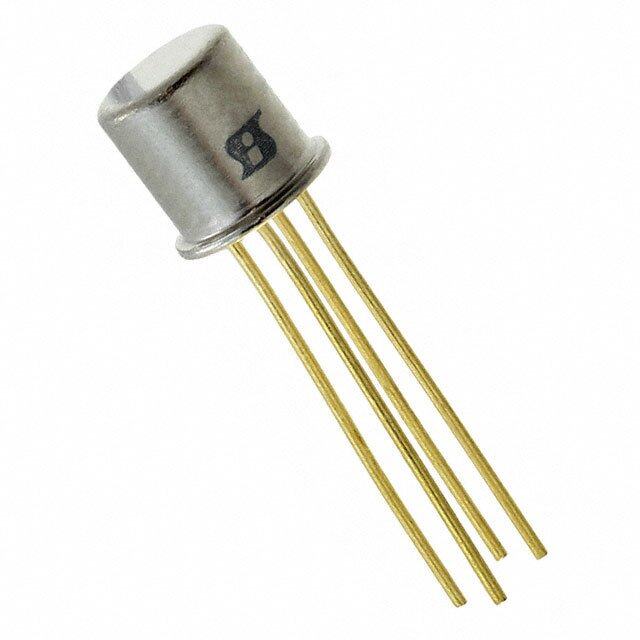
,TO-226_straightlead.jpg)


PDF Datasheet 数据手册内容提取
2N5457, 2N5458 JFETs - General Purpose N−Channel − Depletion N−Channel Junction Field Effect Transistors, depletion mode (Type A) designed for audio and switching applications. http://onsemi.com Features • N−Channel for Higher Gain 1 DRAIN • Drain and Source Interchangeable • High AC Input Impedance 3 • High DC Input Resistance GATE • Low Transfer and Input Capacitance • Low Cross−Modulation and Intermodulation Distortion 2 SOURCE • Plastic Encapsulated Package • Pb−Free Packages are Available* MARKING DIAGRAM MAXIMUM RATINGS 2N Rating Symbol Value Unit 545x AYWW(cid:2) Drain−Source Voltage VDS 25 Vdc (cid:2) Drain−Gate Voltage VDG 25 Vdc 12 1 2 3 3 Reverse Gate−Source Voltage VGSR −25 Vdc STRAIGHT LEAD BENT LEAD Gate Current IG 10 mAdc BULK PACK TAPE & REEL TO−92 TDoetraal tDe eavbioceve D 2is5s°iCpation @ TA = 25°C PD 23.1802 mmWW/°C AMMO PACK CSATYSLEE 2 59 Operating Junction Temperature TJ 135 °C 2N545x =Device Code x = 7 or 8 Storage Temperature Range Tstg −65 to +150 °C A =Assembly Location Stresses exceeding Maximum Ratings may damage the device. Maximum Y =Year Ratings are stress ratings only. Functional operation above the Recommended WW =Work Week Operating Conditions is not implied. Extended exposure to stresses above the (cid:2) =Pb−Free Package Recommended Operating Conditions may affect device reliability. (Note: Microdot may be in either location) ORDERING INFORMATION Device Package Shipping 2N5457 TO−92 1000 Units/Box 2N5457G TO−92 1000 Units/Box (Pb−Free) 2N5458 TO−92 1000 Units/Box 2N5458G TO−92 1000 Units/Box (Pb−Free) *For additional information on our Pb−Free strategy and soldering details, please download the ON Semiconductor Soldering and Mounting Techniques Reference Manual, SOLDERRM/D. © Semiconductor Components Industries, LLC, 2010 1 Publication Order Number: February, 2010 − Rev. 6 2N5457/D
2N5457, 2N5458 ELECTRICAL CHARACTERISTICS (TA = 25°C unless otherwise noted) Characteristic Symbol Min Typ Max Unit OFF CHARACTERISTICS Gate−Source Breakdown Voltage V(BR)GSS (IG = −10 (cid:2)Adc, VDS = 0) −25 − − Vdc Gate Reverse Current IGSS (VGS = −15 Vdc, VDS = 0) − − -(cid:2)1.0 nAdc (VGS = −15 Vdc, VDS = 0, TA = 100°C) − − −200 Gate−Source Cutoff Voltage 2N5457 VGS(off) −0.5 − −6.0 Vdc (VDS = 15 Vdc, iD = 10 nAdc) 2N5458 −1.0 − −7.0 Gate−Source Voltage VGS (VDS = 15 Vdc, iD = 100 (cid:2)Adc) 2N5457 − −2.5 − Vdc (VDS = 15 Vdc, iD = 200 (cid:2)Adc) 2N5458 − −3.5 − ON CHARACTERISTICS Zero−Gate−Voltage Drain Current (Note 1) 2N5457 IDSS 1.0 3.0 5.0 mAdc (VDS = 15 Vdc, VGS = 0) 2N5458 2.0 6.0 9.0 DYNAMIC CHARACTERISTICS Forward Transfer Admittance (Note 1) 2N5457 |Yfs| 1000 3000 5000 (cid:2)mhos (VDS = 15 Vdc, VGS = 0, f = 1 kHz) 2N5458 1500 4000 5500 Output Admittance Common Source (Note 1) |Yos| (VDS = 15 Vdc, VGS = 0, f = 1 kHz) − 10 50 (cid:2)mhos Input Capacitance Ciss (VDS = 15 Vdc, VGS = 0, f = 1 kHz) − 4.5 7.0 pF Reverse Transfer Capacitance Crss (VDS = 15 Vdc, VGS = 0, f = 1 kHz) − 1.5 3.0 pF 1. Pulse Width ≤ 630 ms, Duty Cycle ≤ 10%. http://onsemi.com 2
2N5457, 2N5458 TYPICAL CHARACTERISTICS For 2N5457 Only 14 12 VDS = 15 V VGS = 0 B) f = 1 kHz d 10 E ( R U G 8 FI E OIS 6 N F, N 4 2 0 0.001 0.01 0.1 1.0 10 RS, SOURCE RESISTANCE (Megohms) Figure 1. Noise Figure versus Source Resistance 1.2 1.2 VGS(off) (cid:2) -1.2 V VGS = 0 V VGS(off) (cid:2) -1.2 V 1.0 1.0 A) A) m m T ( 0.8 -(cid:2)0.2 V T ( 0.8 N N E E R R VDS = 15 V R R N CU 0.6 -(cid:2)0.4 V N CU 0.6 AI AI DR 0.4 DR 0.4 , D -(cid:2)0.6 V , D I I 0.2 -(cid:2)0.8 V 0.2 -(cid:2)1.0 V 0 0 0 5 10 15 20 25 -(cid:2)1.2 -(cid:2)0.8 -(cid:2)0.4 0 VDS, DRAIN(cid:2)-(cid:2)SOURCE VOLTAGE (VOLTS) VGS, GATE(cid:2)-(cid:2)SOURCE VOLTAGE (VOLTS) Figure 2. Typical Drain Characteristics Figure 3. Common Source Transfer Characteristics http://onsemi.com 3
2N5457, 2N5458 TYPICAL CHARACTERISTICS For 2N5457 Only 5 5 VGS = 0 V VGS(off) (cid:2) -(cid:2)3.5 V 4 4 A) A) T (m VGS(off) (cid:2) -(cid:2)3.5 V T (m N N E 3 E 3 R -(cid:2)1 V R R R CU CU VDS = 15 V N N AI 2 AI 2 R R D D , D -(cid:2)2 V , D I 1 I 1 -(cid:2)3 V 0 0 0 5 10 15 20 25 -(cid:2)5 -(cid:2)4 -(cid:2)3 -(cid:2)2 -(cid:2)1 0 VDS, DRAIN(cid:2)-(cid:2)SOURCE VOLTAGE (VOLTS) VGS, GATE(cid:2)-(cid:2)SOURCE VOLTAGE (VOLTS) Figure 4. Typical Drain Characteristics Figure 5. Common Source Transfer Characteristics 10 10 VGS(off) (cid:2) -(cid:2)5.8 V VGS = 0 V 8 8 A) VGS(off) (cid:2) -(cid:2)5.8 V A) m m T ( -(cid:2)1 V T ( EN 6 EN 6 R R CUR -(cid:2)2 V CUR VDS = 15 V N 4 N 4 AI AI R R , DD -(cid:2)3 V , DD I 2 I 2 -(cid:2)4 V -(cid:2)5 V 0 0 0 5 10 15 20 25 -(cid:2)7 -(cid:2)6 -(cid:2)5 -(cid:2)4 -(cid:2)3 -(cid:2)2 -(cid:2)1 0 VDS, DRAIN(cid:2)-(cid:2)SOURCE VOLTAGE (VOLTS) VGS, GATE(cid:2)-(cid:2)SOURCE VOLTAGE (VOLTS) Figure 6. Typical Drain Characteristics Figure 7. Common Source Transfer Characteristics NOTE: Note: Graphical data is presented for dc conditions. Tabular data is given for pulsed conditions (Pulse Width = 630 ms, Duty Cycle = 10%). Under dc conditions, self heating in higher IDSS units reduces IDSS. http://onsemi.com 4
MECHANICAL CASE OUTLINE PACKAGE DIMENSIONS TO−92 (TO−226) 1 WATT CASE 29−10 SCALE 1:1 ISSUE A DATE 08 MAY 2012 1 12 2 3 3 STRAIGHT LEAD BENT LEAD A NOTES: STRAIGHT LEAD 1. DIMENSIONING AND TOLERANCING PER ANSI Y14.5M, 1994. B 2. CONTROLLING DIMENSION: INCHES. R 3. CONTOUR OF PACKAGE BEYOND DIMENSION R IS UNCONTROLLED. 4. DIMENSION F APPLIES BETWEEN DIMENSIONS P P AND L. DIMENSIONS D AND J APPLY BETWEEN DI L MENSIONS L AND K MINIMUM. THE LEAD F DIMENSIONS ARE UNCONTROLLED IN DIMENSION K P AND BEYOND DIMENSION K MINIMUM. INCHES MILLIMETERS DIM MIN MAX MIN MAX A 0.175 0.205 4.44 5.21 B 0.290 0.310 7.37 7.87 X X D C 0.125 0.165 3.18 4.19 G D 0.018 0.021 0.46 0.53 H J F 0.016 0.019 0.41 0.48 G 0.045 0.055 1.15 1.39 V C HJ 00..009158 00..100254 20..4426 20..6661 SECTION X−X K 0.500 --- 12.70 --- 1 N L 0.250 --- 6.35 --- N 0.080 0.105 2.04 2.66 N P --- 0.100 --- 2.54 R 0.135 --- 3.43 --- V 0.135 --- 3.43 --- A NOTES: R BENT LEAD 1. DIMENSIONING AND TOLERANCING PER ASME Y14.5M, 1994. B 2. CONTROLLING DIMENSION: INCHES. 3. CONTOUR OF PACKAGE BEYOND DIMENSION R IS UNCONTROLLED. 4. DIMENSION F APPLIES BETWEEN DIMENSIONS P P AND L. DIMENSIONS D AND J APPLY BETWEEN T DIMENSIONS L AND K MINIMUM. THE LEAD DIMENSIONS ARE UNCONTROLLED IN DIMENSION SPELAATNIENG K P AND BEYOND DIMENSION K MINIMUM. INCHES MILLIMETERS DIM MIN MAX MIN MAX A 0.175 0.205 4.44 5.21 B 0.290 0.310 7.37 7.87 X X D C 0.125 0.165 3.18 4.19 G D 0.018 0.021 0.46 0.53 J G 0.094 0.102 2.40 2.80 J 0.018 0.024 0.46 0.61 V K 0.500 --- 12.70 --- C N 0.080 0.105 2.04 2.66 SECTION X−X P --- 0.100 --- 2.54 1 N R 0.135 --- 3.43 --- V 0.135 --- 3.43 --- STYLES ON PAGE 2 Electronic versions are uncontrolled except when accessed directly from the Document Repository. DOCUMENT NUMBER: 98AON52857E Printed versions are uncontrolled except when stamped “CONTROLLED COPY” in red. DESCRIPTION: TO−92 (TO−226) 1 WATT PAGE 1 OF 2 ON Semiconductor and are trademarks of Semiconductor Components Industries, LLC dba ON Semiconductor or its subsidiaries in the United States and/or other countries. ON Semiconductor reserves the right to make changes without further notice to any products herein. ON Semiconductor makes no warranty, representation or guarantee regarding the suitability of its products for any particular purpose, nor does ON Semiconductor assume any liability arising out of the application or use of any product or circuit, and specifically disclaims any and all liability, including without limitation special, consequential or incidental damages. ON Semiconductor does not convey any license under its patent rights nor the rights of others. © Semiconductor Components Industries, LLC, 2019 www.onsemi.com
TO−92 (TO−226) 1 WATT CASE 29−10 ISSUE A DATE 08 MAY 2012 STYLE 1: STYLE 2: STYLE 3: STYLE 4: STYLE 5: PIN 1. EMITTER PIN 1. BASE PIN 1. ANODE PIN 1. CATHODE PIN 1. DRAIN 2. BASE 2. EMITTER 2. ANODE 2. CATHODE 2. SOURCE 3. COLLECTOR 3. COLLECTOR 3. CATHODE 3. ANODE 3. GATE STYLE 6: STYLE 7: STYLE 8: STYLE 9: STYLE 10: PIN 1. GATE PIN 1. SOURCE PIN 1. DRAIN PIN 1. BASE 1 PIN 1. CATHODE 2. SOURCE & SUBSTRATE 2. DRAIN 2. GATE 2. EMITTER 2. GATE 3. DRAIN 3. GATE 3. SOURCE & SUBSTRATE 3. BASE 2 3. ANODE STYLE 11: STYLE 12: STYLE 13: STYLE 14: STYLE 15: PIN 1. ANODE PIN 1. MAIN TERMINAL 1 PIN 1. ANODE 1 PIN 1. EMITTER PIN 1. ANODE 1 2. CATHODE & ANODE 2. GATE 2. GATE 2. COLLECTOR 2. CATHODE 3. CATHODE 3. MAIN TERMINAL 2 3. CATHODE 2 3. BASE 3. ANODE 2 STYLE 16: STYLE 17: STYLE 18: STYLE 19: STYLE 20: PIN 1. ANODE PIN 1. COLLECTOR PIN 1. ANODE PIN 1. GATE PIN 1. NOT CONNECTED 2. GATE 2. BASE 2. CATHODE 2. ANODE 2. CATHODE 3. CATHODE 3. EMITTER 3. NOT CONNECTED 3. CATHODE 3. ANODE STYLE 21: STYLE 22: STYLE 23: STYLE 24: STYLE 25: PIN 1. COLLECTOR PIN 1. SOURCE PIN 1. GATE PIN 1. EMITTER PIN 1. MT 1 2. EMITTER 2. GATE 2. SOURCE 2. COLLECTOR/ANODE 2. GATE 3. BASE 3. DRAIN 3. DRAIN 3. CATHODE 3. MT 2 STYLE 26: STYLE 27: STYLE 28: STYLE 29: STYLE 30: PIN 1. VCC PIN 1. MT PIN 1. CATHODE PIN 1. NOT CONNECTED PIN 1. DRAIN 2. GROUND 2 2. SUBSTRATE 2. ANODE 2. ANODE 2. GATE 3. OUTPUT 3. MT 3. GATE 3. CATHODE 3. SOURCE STYLE 31: STYLE 32: STYLE 33: STYLE 34: STYLE 35: PIN 1. GATE PIN 1. BASE PIN 1. RETURN PIN 1. INPUT PIN 1. GATE 2. DRAIN 2. COLLECTOR 2. INPUT 2. GROUND 2. COLLECTOR 3. SOURCE 3. EMITTER 3. OUTPUT 3. LOGIC 3. EMITTER Electronic versions are uncontrolled except when accessed directly from the Document Repository. DOCUMENT NUMBER: 98AON52857E Printed versions are uncontrolled except when stamped “CONTROLLED COPY” in red. DESCRIPTION: TO−92 (TO−226) 1 WATT PAGE 2 OF 2 ON Semiconductor and are trademarks of Semiconductor Components Industries, LLC dba ON Semiconductor or its subsidiaries in the United States and/or other countries. ON Semiconductor reserves the right to make changes without further notice to any products herein. ON Semiconductor makes no warranty, representation or guarantee regarding the suitability of its products for any particular purpose, nor does ON Semiconductor assume any liability arising out of the application or use of any product or circuit, and specifically disclaims any and all liability, including without limitation special, consequential or incidental damages. ON Semiconductor does not convey any license under its patent rights nor the rights of others. © Semiconductor Components Industries, LLC, 2019 www.onsemi.com
ON Semiconductor and are trademarks of Semiconductor Components Industries, LLC dba ON Semiconductor or its subsidiaries in the United States and/or other countries. ON Semiconductor owns the rights to a number of patents, trademarks, copyrights, trade secrets, and other intellectual property. A listing of ON Semiconductor’s product/patent coverage may be accessed at www.onsemi.com/site/pdf/Patent−Marking.pdf. ON Semiconductor reserves the right to make changes without further notice to any products herein. ON Semiconductor makes no warranty, representation or guarantee regarding the suitability of its products for any particular purpose, nor does ON Semiconductor assume any liability arising out of the application or use of any product or circuit, and specifically disclaims any and all liability, including without limitation special, consequential or incidental damages. Buyer is responsible for its products and applications using ON Semiconductor products, including compliance with all laws, regulations and safety requirements or standards, regardless of any support or applications information provided by ON Semiconductor. “Typical” parameters which may be provided in ON Semiconductor data sheets and/or specifications can and do vary in different applications and actual performance may vary over time. All operating parameters, including “Typicals” must be validated for each customer application by customer’s technical experts. ON Semiconductor does not convey any license under its patent rights nor the rights of others. ON Semiconductor products are not designed, intended, or authorized for use as a critical component in life support systems or any FDA Class 3 medical devices or medical devices with a same or similar classification in a foreign jurisdiction or any devices intended for implantation in the human body. Should Buyer purchase or use ON Semiconductor products for any such unintended or unauthorized application, Buyer shall indemnify and hold ON Semiconductor and its officers, employees, subsidiaries, affiliates, and distributors harmless against all claims, costs, damages, and expenses, and reasonable attorney fees arising out of, directly or indirectly, any claim of personal injury or death associated with such unintended or unauthorized use, even if such claim alleges that ON Semiconductor was negligent regarding the design or manufacture of the part. ON Semiconductor is an Equal Opportunity/Affirmative Action Employer. This literature is subject to all applicable copyright laws and is not for resale in any manner. PUBLICATION ORDERING INFORMATION LITERATURE FULFILLMENT: TECHNICAL SUPPORT Email Requests to: orderlit@onsemi.com North American Technical Support: Europe, Middle East and Africa Technical Support: Voice Mail: 1 800−282−9855 Toll Free USA/Canada Phone: 00421 33 790 2910 ON Semiconductor Website: www.onsemi.com Phone: 011 421 33 790 2910 For additional information, please contact your local Sales Representative ◊ www.onsemi.com 1