ICGOO在线商城 > 分立半导体产品 > 晶体管 - FET,MOSFET - 阵列 > ZXMHC10A07T8TA
 Datasheet下载
- 型号: ZXMHC10A07T8TA
- 制造商: Diodes Inc.
- 库位|库存: xxxx|xxxx
- 要求:
| 数量阶梯 | 香港交货 | 国内含税 |
| +xxxx | $xxxx | ¥xxxx |
查看当月历史价格
查看今年历史价格
ZXMHC10A07T8TA产品简介:
ICGOO电子元器件商城为您提供ZXMHC10A07T8TA由Diodes Inc.设计生产,在icgoo商城现货销售,并且可以通过原厂、代理商等渠道进行代购。 ZXMHC10A07T8TA价格参考。Diodes Inc.ZXMHC10A07T8TA封装/规格:晶体管 - FET,MOSFET - 阵列, 2 个 N 通道和 2 个 P 通道(H 桥) Mosfet 阵列 100V 1A,800mA 1.3W 表面贴装 SM8。您可以下载ZXMHC10A07T8TA参考资料、Datasheet数据手册功能说明书,资料中有ZXMHC10A07T8TA 详细功能的应用电路图电压和使用方法及教程。
ZXMHC10A07T8TA 是由 Diodes Incorporated 生产的一款晶体管 - FET,MOSFET - 阵列型号。以下是该型号的一些典型应用场景:

 1. 电源管理
   - ZXMHC10A07T8TA 常用于高效的电源管理系统中,例如 DC-DC 转换器、负载开关和电压调节模块。其低导通电阻(Rds(on))特性可以减少功率损耗,提高整体效率。
   - 在电池供电设备中,该器件可用于电池充电管理、放电保护以及电量监测电路。

 2. 电机驱动
   - 适用于小型直流电机或步进电机的驱动电路。通过精确控制 MOSFET 的开关状态,实现对电机速度和方向的调节。
   - 其阵列结构支持多通道独立控制,适合需要同时驱动多个电机的应用场景。

 3. 消费类电子产品
   - 广泛应用于智能手机、平板电脑、笔记本电脑等便携式电子设备中的信号切换和电源路径管理。
   - 在音频设备中,可作为功率放大器的开关元件,提供稳定的电流输出。

 4. 工业自动化
   - 用于工业控制中的继电器替代方案,实现快速、可靠的开关操作。
   - 在传感器接口电路中,用作信号隔离或增强驱动能力的组件。

 5. 通信设备
   - 在基站、路由器和其他通信设备中,该 MOSFET 阵列可用于信号路由、天线切换以及电源分配网络。

 6. 汽车电子
   - 可用于车载信息娱乐系统、LED 照明驱动以及电动座椅调节等功能模块中。
   - 在新能源汽车中,该器件可能参与电池管理系统 (BMS) 或辅助逆变器的设计。

 特性总结:
- 低导通电阻:降低功耗,提升效率。
- 高可靠性:适合严苛环境下的长期运行。
- 紧凑封装:节省 PCB 空间,便于小型化设计。

综上所述,ZXMHC10A07T8TA 凭借其高性能和灵活性,适用于多种领域,包括消费电子、工业控制、通信设备及汽车电子等。具体应用需根据实际需求选择合适的外围电路和参数配置。
| 参数 | 数值 |
| 产品目录 | |
| ChannelMode | Enhancement |
| 描述 | MOSFET 2N/2P-CH 100V 1A/0.8A SM8MOSFET 100V 1.4A N-Channel MOSFET H-Bridge |
| 产品分类 | FET - 阵列分离式半导体 |
| FET功能 | 标准 |
| FET类型 | 2 个 N 通道和 2 个 P 通道(H 桥) |
| Id-ContinuousDrainCurrent | 1.1 A |
| Id-连续漏极电流 | 1.1 A |
| 品牌 | Diodes Incorporated |
| 产品手册 | |
| 产品图片 |
|
| rohs | 符合RoHS无铅 / 符合限制有害物质指令(RoHS)规范要求 |
| 产品系列 | 晶体管,MOSFET,Diodes Incorporated ZXMHC10A07T8TA- |
| 数据手册 | |
| 产品型号 | ZXMHC10A07T8TA |
| Pd-PowerDissipation | 1.3 W |
| Pd-功率耗散 | 1.3 W |
| Qg-GateCharge | 2.9 nC, 3.5 nC |
| Qg-栅极电荷 | 2.9 nC, 3.5 nC |
| RdsOn-Drain-SourceResistance | 700 mOhms at N Channel, 1000 mOhms at P Channel |
| RdsOn-漏源导通电阻 | 700 mOhms, 1 Ohms |
| RoHS指令信息 | http://diodes.com/download/4349 |
| Vds-Drain-SourceBreakdownVoltage | 100 V |
| Vds-漏源极击穿电压 | 100 V |
| Vgs-栅源极击穿电压 | 20 V |
| Vgsth-Gate-SourceThresholdVoltage | 2 V |
| Vgsth-栅源极阈值电压 | 2 V |
| 上升时间 | 1.5 ns, 2.1 ns |
| 下降时间 | 2.1 ns, 3.3 ns |
| 不同Id时的Vgs(th)(最大值) | 4V @ 250µA |
| 不同Vds时的输入电容(Ciss) | 138pF @ 60V |
| 不同Vgs时的栅极电荷(Qg) | 2.9nC @ 10V |
| 不同 Id、Vgs时的 RdsOn(最大值) | 700 毫欧 @ 1.5A,10V |
| 产品目录页面 | |
| 产品种类 | MOSFET |
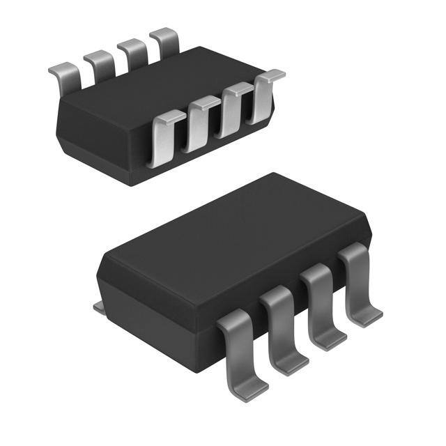
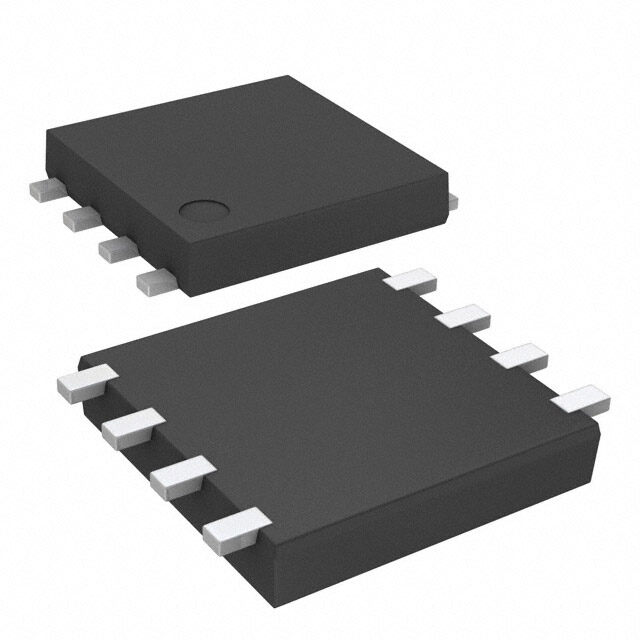
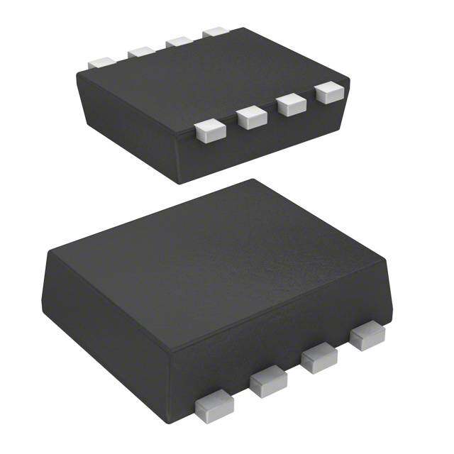
| 供应商器件封装 | SM8 |
| 其它名称 | ZXMHC10A07T8DKR |
| 典型关闭延迟时间 | 4.1 ns, 5.9 ns |
| 功率-最大值 | 1.3W |
| 包装 | Digi-Reel® |
| 商标 | Diodes Incorporated |
| 安装类型 | 表面贴装 |
| 安装风格 | SMD/SMT |
| 封装 | Reel |
| 封装/外壳 | SOT-223-8 |
| 封装/箱体 | SM-8 |
| 工厂包装数量 | 1000 |
| 晶体管极性 | N and P-Channel |
| 最大工作温度 | + 150 C |
| 最小工作温度 | - 55 C |
| 标准包装 | 1 |
| 正向跨导-最小值 | 1.6 S, 1.2 S |
| 漏源极电压(Vdss) | 100V |
| 电流-连续漏极(Id)(25°C时) | 1A,800mA |
| 通道模式 | Enhancement |
| 配置 | Half-Bridge |


- 商务部:美国ITC正式对集成电路等产品启动337调查
- 曝三星4nm工艺存在良率问题 高通将骁龙8 Gen1或转产台积电
- 太阳诱电将投资9.5亿元在常州建新厂生产MLCC 预计2023年完工
- 英特尔发布欧洲新工厂建设计划 深化IDM 2.0 战略
- 台积电先进制程称霸业界 有大客户加持明年业绩稳了
- 达到5530亿美元!SIA预计今年全球半导体销售额将创下新高
- 英特尔拟将自动驾驶子公司Mobileye上市 估值或超500亿美元
- 三星加码芯片和SET,合并消费电子和移动部门,撤换高东真等 CEO
- 三星电子宣布重大人事变动 还合并消费电子和移动部门
- 海关总署:前11个月进口集成电路产品价值2.52万亿元 增长14.8%


PDF Datasheet 数据手册内容提取
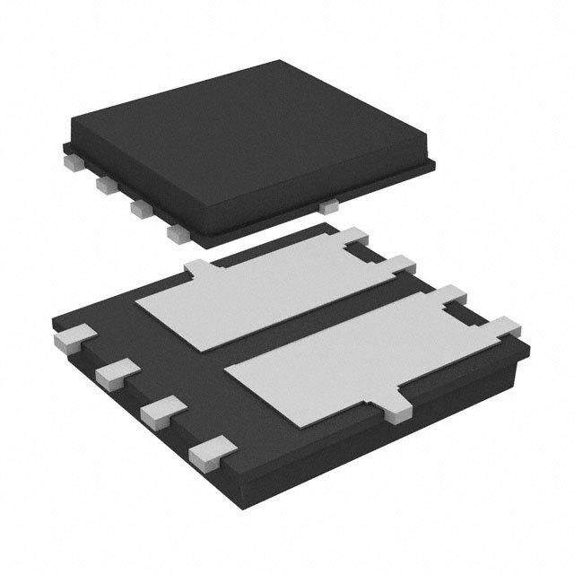
ZXMHC10A07T8 Green COMPLEMENTARY 100V ENHANCEMENT MODE MOSFET H-BRIDGE Product Summary Features Device BVDSS RDS(ON) max TAI D= m+2a5x° C 2L oxw N O +n -2R xe sPi sCtahnacnen els in a SOIC Package 0.7Ω @ VGS = 10V 1.4A Low Input Capacitance N-Channel 100V T 0.9Ω @ VGS = 6V 1.1A Fast Switching Speed CON P-Channel -100V 1.0Ω @ VGS = -10V -1.3A Lead-Free Finish; RoHS Compliant (Notes 1 & 2) U 1.45Ω @ VGS = -6V -0.9A Halogen and Antimony Free. “Green” Device (Note 3) DTI OA Description Mechanical Data RM PR This new generation complementary MOSFET H-Bridge features low Case: SM-8 (8 LEAD SOT223) W O on-resistance achievable with low gate drive. Case Material: Molded Plastic, "Green" Molding Compound; F E UL Flammability Classification Rating 94V-0 N N Moisture Sensitivity: Level 1 per J-STD-020 I Applications Terminal Connections Indicator: See Diagram E C DC Motor Control Terminals: Finish Matte Tin Annealed over Copper Leadframe; N DC-AC Inverters Solderable per MIL-STD-202, Method 208 A Weight: 0.117 grams (Approximate) V D A SM-8 PIN1 G3 G4 S2 S3 D3 D4 G2 S1S4 G1 D1 D2 Top View Pin CToopn fVigiuerwa tion Internal Schematic Ordering Information (Note 4) Part Number Reel Size Tape Width Quantity per Reel ZXMHC10A07T8TA 7’’ 12mm 1,000 units Notes: 1. EU Directive 2002/95/EC (RoHS) & 2011/65/EU (RoHS 2) compliant. All applicable RoHS exemptions applied. 2. See http://www.diodes.com/quality/lead_free.html for more information about Diodes Incorporated’s definitions of Halogen- and Antimony-free, "Green" and Lead-free. 3. Halogen- and Antimony-free "Green” products are defined as those which contain <900ppm bromine, <900ppm chlorine (<1500ppm total Br + Cl) and <1000ppm antimony compounds. 4. For packaging details, go to our website at http://www.diodes.com/products/packages.html. Marking Information SM-8 ZXMHC10A07 = Product Type Marking Code ZXMHC W YWW = Date Code Marking 10A07 W Y or Y = Last Digit of Year (ex: 5= 2015) Y WW or WW = Week Code (01~53) ZXMHC10A07T8 1 of 10 March 2015 Document number: DS33510 Rev. 4 - 2 www.diodes.com © Diodes Incorporated
ZXMHC10A07T8 Maximum Ratings (@TA = +25°C, unless otherwise specified.) Characteristic Symbol N-channel P-channel Units Drain-Source Voltage VDSS 100 -100 V Gate-Source Voltage VGSS ±20 ±20 V TA = +25°C (Note 6) 1.1 -0.9 Steady Continuous Drain Current, VGS = 10V (Note 8) State TA = +70°C (Note 6) ID 0.9 -0.8 A T TA = +25°C (Note 5) 1.0 -0.8 CN Maximum Body Diode Forward Current (Note 6) IS 2.3 -2.2 A O U Pulsed Drain Current (Note 7) IDM 5.2 -4.5 A I DT Pulsed Source Current (Note 7) ISM 5.2 -4.5 A OA RM POR Thermal Characteristics (@TA = +25°C, unless otherwise specified.) W F Characteristic Symbol Value Units E N Total Power Dissipation (Note 8) 1.3 W N I Linear Derating Factor TA = +25°C (Note 5) PD 10.4 mW/°C E Total Power Dissipation (Note 8) 1.3 W C Linear Derating Factor TA = +25°C (Note 6) PD mW/°C N Steady State (Note 5) 94.5 °C/W A Thermal Resistance, Junction to Ambient (Note 8) Steady State (Note 6) RθJA 73.3 °C/W V D Operating and Storage Temperature Range TJ, TSTG -55 to +150 °C A Notes: 5. For a device surface mounted on 50mm x 50mm x 1.6mm FR4 PCB with high coverage of single sided 2oz copper, in still air conditions, with the heat sink split into two equal areas one for each drain connection. 6. For a device surface mounted on FR4 PCB measured at t 10 seconds. 7. Repetitive rating 50mm x 50mm x 1.6mm FR4 PCB, D = 0.02, pulse width 300μs - pulse width limited by maximum junction temperature. Refer to Transient Thermal Impedance graph. 8. For device with one active die. ZXMHC10A07T8 2 of 10 March 2015 Document number: DS33510 Rev. 4 - 2 www.diodes.com © Diodes Incorporated
ZXMHC10A07T8 Electrical Characteristics N-CHANNEL (@TA = +25°C, unless otherwise specified.) Characteristic Symbol Min Typ Max Unit Test Condition OFF CHARACTERISTICS (Note 10) Drain-Source Breakdown Voltage BVDSS 100 — — V VGS = 0V, ID = 250μA Zero Gate Voltage Drain Current IDSS — — 1.0 μA VDS = 100V, VGS = 0V Gate-Source Leakage IGSS — — 100 nA VGS = ±20V, VDS = 0V ON CHARACTERISTICS (Note 10) T N Gate Threshold Voltage VGS(TH) 2.0 — 4.0 V VDS = VGS, ID = 250μA UCIO Static Drain-Source On-Resistance (Note 9) RDS(ON) —— —— 00..79 Ω VVGGSS == 16.00VV, ,I IDD = = 1 1..50AA DT Forward Transfer Admittance (Notes 9 & 11) gfs — 1.6 — S VDS = 15V, ID = 1.0A ROMA DDiYoNdeA MFoICrw CarHdA VRoAltCagTeE (RNISotTeI C9)S (Note 11) VSD — — 0.95 V VGS = 0V, IS = 1.5A PR Input Capacitance Ciss — 138 — W FO Output Capacitance Coss — 12 — pF Vf =D S1 M= H60zV , VGS = 0V, EN Reverse Transfer Capacitance Crss — 6 — NE I TGoattael- SGoauterc Ceh Cahrgaerg e QQggs —— 20..97 —— nC V10DVS = 50V, ID = 1.0A, VGS = C Gate-Drain Charge Qgd — 1.0 — N Turn-On Delay Time tD(ON) — 1.8 — A Turn-On Rise Time tR — 1.5 — ns VDD = 50V, VGS = 10V, V Turn-Off Delay Time tD(OFF) — 4.1 — ID = 1.0A, RG = 6.0Ω D Turn-Off Fall Time tF — 2.1 — A RReevveerrssee RReeccoovveerryy TCihmaerg e tQRRrr —— 2172 —— nnCs IS = 1.8A, di/dt = 100A/μs Electrical Characteristics P-CHANNEL (@TA = +25°C, unless otherwise specified.) Characteristic Symbol Min Typ Max Unit Test Condition OFF CHARACTERISTICS (Note 10) Drain-Source Breakdown Voltage BVDSS -100 — — V VGS = 0V, ID = -250μA Zero Gate Voltage Drain Current IDSS — — -1.0 μA VDS = -100V, VGS = 0V Gate-Source Leakage IGSS — — 100 nA VGS = ±20V, VDS = 0V ON CHARACTERISTICS (Note 10) Gate Threshold Voltage VGS(TH) -2.0 — -4.0 V VDS = VGS, ID = -250μA Static Drain-Source On-Resistance (Note 9) RDS(ON) —— —— 11.4.05 Ω VVGGSS == --16.00VV,, IIDD == - -00.6.5AA Forward Transfer Admittance (Notes 9 & 11) gfs — 1.2 — S VDS = -15V, ID = -0.6A Diode Forward Voltage (Note 9) VSD — -0.85 -0.95 V VGS = 0V, IS = -0.75A DYNAMIC CHARACTERISTICS (Note 11) Input Capacitance Ciss — 141 — pF Output Capacitance Coss — 13.1 — pF Vf =D S1 M= H-5z0 V , VGS = 0V, Reverse Transfer Capacitance Crss — 10.8 — pF Gate Charge (VGS = -5.0V) Qg — 1.6 — nC TGoattael- SGoauterc Ceh Cahrgaerg (eV GS = -10V) QQggs —— 30..56 —— nnCC VDS = -50V, ID = -0.6A Gate-Drain Charge Qgd — 1.6 — nC Turn-On Delay Time tD(ON) — 1.6 — ns Turn-On Rise Time tR — 2.1 — ns VDD = -50V, VGS = -10V, Turn-Off Delay Time tD(OFF) — 5.9 — ns RG = 6.0Ω, ID = -1.0A Turn-Off Fall Time tF — 3.3 — ns RReevveerrssee RReeccoovveerryy TCihmaerg e tQRRrr —— 2391 —— nnCs IS = -0.9A, di/dt = 100A/μs Notes: 9. Measured under pulsed conditions. Width≤300μs. Duty cycle ≤ 2%. 10. Short duration pulse test used to minimize self-heating effect. 11. Guaranteed by design. Not subject to product testing. ZXMHC10A07T8 3 of 10 March 2015 Document number: DS33510 Rev. 4 - 2 www.diodes.com © Diodes Incorporated
ZXMHC10A07T8 Typical Characteristics T N C O U I DT OA RM PR O W F E N N I E C N A V D A ZXMHC10A07T8 4 of 10 March 2015 Document number: DS33510 Rev. 4 - 2 www.diodes.com © Diodes Incorporated
ZXMHC10A07T8 Typical Characteristics (N-Channel) T N C O U I DT OA RM PR O W F E N N I E C N A V D A ZXMHC10A07T8 5 of 10 March 2015 Document number: DS33510 Rev. 4 - 2 www.diodes.com © Diodes Incorporated
ZXMHC10A07T8 Typical Characteristics (N-Channel) (Cont.) T N C O U I DT OA RM PR O W F E N N I E C N A V D A ZXMHC10A07T8 6 of 10 March 2015 Document number: DS33510 Rev. 4 - 2 www.diodes.com © Diodes Incorporated
ZXMHC10A07T8 Typical Characteristics (P-Channel) T N C O U I DT OA RM PR O W F E N N I E C N A V D A ZXMHC10A07T8 7 of 10 March 2015 Document number: DS33510 Rev. 4 - 2 www.diodes.com © Diodes Incorporated
ZXMHC10A07T8 Typical Characteristics (P-Channel) (Cont.) T N C O U I DT OA RM PR O W F E N N I E C N A V D A ZXMHC10A07T8 8 of 10 March 2015 Document number: DS33510 Rev. 4 - 2 www.diodes.com © Diodes Incorporated
ZXMHC10A07T8 Package Outline Dimensions Please see AP02002 at http://www.diodes.com/datasheets/ap02002.pdf for the latest version. A1 A Seating Plane T SM-8 N C Dim Min Max Typ O U A -- 1.70 1.60 DTI D A1 0.02 0.10 0.04 OA e1 b 0.70 0.90 0.80 RM c 0.24 0.32 0.28 L D 6.30 6.70 6.60 PR e 1.53 REF O W e1 4.59 REF F EN ø E 6.70 7.30 7.00 N E1 3.30 3.70 3.50 I E E E1 ØL 0.-7- 5 1.-0- 0 04.59°0 C Ø1 -- 15° -- N ø1 c Ø2 -- -- 10° A All Dimensions in mm V D A b e ø2 Suggested Pad Layout Please see AP02001 at http://www.diodes.com/datasheets/ap02001.pdf for the latest version. Y Dimensions Value (in mm) C 1.52 C1 4.60 C1 Y1 X 0.95 Y 2.80 Y1 6.80 X C ZXMHC10A07T8 9 of 10 March 2015 Document number: DS33510 Rev. 4 - 2 www.diodes.com © Diodes Incorporated
ZXMHC10A07T8 IMPORTANT NOTICE DIODES INCORPORATED MAKES NO WARRANTY OF ANY KIND, EXPRESS OR IMPLIED, WITH REGARDS TO THIS DOCUMENT, INCLUDING, BUT NOT LIMITED TO, THE IMPLIED WARRANTIES OF MERCHANTABILITY AND FITNESS FOR A PARTICULAR PURPOSE (AND THEIR EQUIVALENTS UNDER THE LAWS OF ANY JURISDICTION). Diodes Incorporated and its subsidiaries reserve the right to make modifications, enhancements, improvements, corrections or other changes without further notice to this document and any product described herein. Diodes Incorporated does not assume any liability arising out of the T N atrpapdleicmaatiorkn riogrh utss,e n oorf tthheis ridgohctsu mofe ontth oerr sa. n yA npyr oCduusctto dmeesrc orirb eudse hr eorfe tihni;s n deoitchuemr ednote osr Dpirooddeusc tIsn cdoerspcorirbaetedd h ceorenivne iyn asnuyc hli caepnpsliec autinodnes rs ihtsa lpl aatsesnutm oer CO all risks of such use and will agree to hold Diodes Incorporated and all the companies whose products are represented on Diodes Incorporated U website, harmless against all damages. I DT OA Diodes Incorporated does not warrant or accept any liability whatsoever in respect of any products purchased through unauthorized sales channel. RM Should Customers purchase or use Diodes Incorporated products for any unintended or unauthorized application, Customers shall indemnify and hold Diodes Incorporated and its representatives harmless against all claims, damages, expenses, and attorney fees arising out of, directly or PR indirectly, any claim of personal injury or death associated with such unintended or unauthorized application. W O F Products described herein may be covered by one or more United States, international or foreign patents pending. Product names and markings E N noted herein may also be covered by one or more United States, international or foreign trademarks. N I E This document is written in English but may be translated into multiple languages for reference. Only the English version of this document is the final and determinative format released by Diodes Incorporated. C N LIFE SUPPORT A V Diodes Incorporated products are specifically not authorized for use as critical components in life support devices or systems without the express D written approval of the Chief Executive Officer of Diodes Incorporated. As used herein: A A. Life support devices or systems are devices or systems which: 1. are intended to implant into the body, or 2. support or sustain life and whose failure to perform when properly used in accordance with instructions for use provided in the labeling can be reasonably expected to result in significant injury to the user. B. A critical component is any component in a life support device or system whose failure to perform can be reasonably expected to cause the failure of the life support device or to affect its safety or effectiveness. Customers represent that they have all necessary expertise in the safety and regulatory ramifications of their life support devices or systems, and acknowledge and agree that they are solely responsible for all legal, regulatory and safety-related requirements concerning their products and any use of Diodes Incorporated products in such safety-critical, life support devices or systems, notwithstanding any devices- or systems-related information or support that may be provided by Diodes Incorporated. Further, Customers must fully indemnify Diodes Incorporated and its representatives against any damages arising out of the use of Diodes Incorporated products in such safety-critical, life support devices or systems. Copyright © 2015, Diodes Incorporated www.diodes.com ZXMHC10A07T8 10 of 10 March 2015 Document number: DS33510 Rev. 4 - 2 www.diodes.com © Diodes Incorporated
Mouser Electronics Authorized Distributor Click to View Pricing, Inventory, Delivery & Lifecycle Information: D iodes Incorporated: ZXMHC10A07T8TA