ICGOO在线商城 > 分立半导体产品 > 晶体管 - 双极 (BJT) - 阵列 - 预偏置 > XN0111F00L
 Datasheet下载
- 型号: XN0111F00L
- 制造商: Panasonic Corporation
- 库位|库存: xxxx|xxxx
- 要求:
| 数量阶梯 | 香港交货 | 国内含税 |
| +xxxx | $xxxx | ¥xxxx |
查看当月历史价格
查看今年历史价格
XN0111F00L产品简介:
ICGOO电子元器件商城为您提供XN0111F00L由Panasonic Corporation设计生产,在icgoo商城现货销售,并且可以通过原厂、代理商等渠道进行代购。 XN0111F00L价格参考。Panasonic CorporationXN0111F00L封装/规格:晶体管 - 双极 (BJT) - 阵列 - 预偏置, Pre-Biased Bipolar Transistor (BJT) 2 个 PNP 预偏压式(双) 50V 100mA 80MHz 300mW 表面贴装 迷你型5-G1。您可以下载XN0111F00L参考资料、Datasheet数据手册功能说明书,资料中有XN0111F00L 详细功能的应用电路图电压和使用方法及教程。
型号为XN0111F00L的Panasonic Electronic Components品牌双极晶体管(BJT)阵列,属于预偏置型晶体管,主要应用于需要高效、稳定信号处理和功率控制的电子设备中。该器件集成了多个BJT晶体管,并内置偏置电路,简化了外围电路设计,提高了系统稳定性。

XN0111F00L常见应用场景包括:

1. 电源管理电路:用于DC-DC转换器、稳压器等电路中,实现高效能的功率控制。
2. 马达驱动:在小型电机或步进电机驱动电路中作为开关元件,提供稳定的电流放大和控制。
3. 工业自动化设备:用于PLC、传感器接口、继电器驱动等工业控制系统中,提升响应速度与可靠性。
4. 消费类电子产品:如电视、音响、家用电器等,用于音频放大、开关控制或信号处理。
5. 汽车电子:适用于车载电源系统、车灯控制模块、电动窗驱动等对可靠性要求较高的场景。

由于其集成化设计和预偏置特性,XN0111F00L在降低设计复杂度的同时,也减少了PCB空间占用,适用于高密度、高性能要求的电子系统。
| 参数 | 数值 |
| 产品目录 | |
| 描述 | TRANS PREBIAS DUAL PNP MINI5 |
| 产品分类 | 晶体管(BJT) - 阵列﹐预偏压式 |
| 品牌 | Panasonic Electronic Components |
| 数据手册 | http://industrial.panasonic.com/www-cgi/jvcr13pz.cgi?E+SC+4+BFA7001+XN0111F+8+WW |
| 产品图片 |
|
| 产品型号 | XN0111F00L |
| rohs | 含铅 / 不符合限制有害物质指令(RoHS)规范要求 |
| 产品系列 | - |
| 不同 Ib、Ic时的 Vce饱和值(最大值) | 250mV @ 300µA, 10mA |
| 不同 Ic、Vce 时的DC电流增益(hFE)(最小值) | 30 @ 5mA,10V |
| 产品目录绘图 |
|
| 产品目录页面 | |
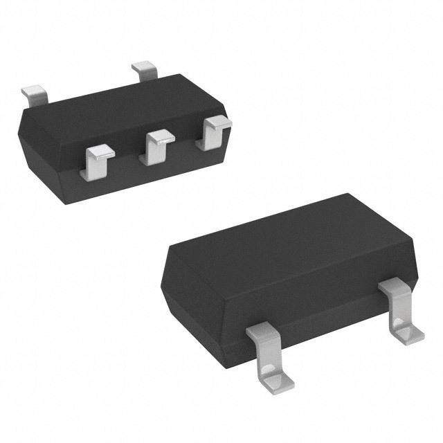
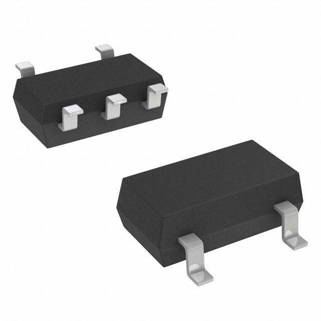
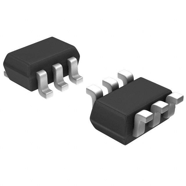
| 供应商器件封装 | 迷你型5-G1 |
| 其它名称 | XN0111F00LTR |
| 功率-最大值 | 300mW |
| 包装 | 带卷 (TR) |
| 安装类型 | 表面贴装 |
| 封装/外壳 | SC-74A,SOT-753 |
| 晶体管类型 | 2 个 PNP 预偏压式(双) |
| 标准包装 | 3,000 |
| 电压-集射极击穿(最大值) | 50V |
| 电流-集电极(Ic)(最大值) | 100mA |
| 电流-集电极截止(最大值) | 500nA |
| 电阻器-发射极基底(R2)(Ω) | 10k |
| 电阻器-基底(R1)(Ω) | 4.7k |
| 频率-跃迁 | 80MHz |


- 商务部:美国ITC正式对集成电路等产品启动337调查
- 曝三星4nm工艺存在良率问题 高通将骁龙8 Gen1或转产台积电
- 太阳诱电将投资9.5亿元在常州建新厂生产MLCC 预计2023年完工
- 英特尔发布欧洲新工厂建设计划 深化IDM 2.0 战略
- 台积电先进制程称霸业界 有大客户加持明年业绩稳了
- 达到5530亿美元!SIA预计今年全球半导体销售额将创下新高
- 英特尔拟将自动驾驶子公司Mobileye上市 估值或超500亿美元
- 三星加码芯片和SET,合并消费电子和移动部门,撤换高东真等 CEO
- 三星电子宣布重大人事变动 还合并消费电子和移动部门
- 海关总署:前11个月进口集成电路产品价值2.52万亿元 增长14.8%


PDF Datasheet 数据手册内容提取
This product complies with the RoHS Directive (EU 2002/95/EC). Composite Transistors XN0111F (XN111F) Silicon PNP epitaxial planar type Unit: mm For switching/digital circuits /21.9.90±+–000...10250 0.16+–00..0160 (0.95) (0.95) e ■ Features 3 4 5 •T(Ewmoi tetleerm-ceonutpsl eindc torrapnosriasttoedrs iwntioth o bnue iplta-icnk aregseistor) c d +0.251.50–0.05+0.22.8–0.3 5˚ 0.4±0.2 •Reduction of the mounting area and assembly cost bny one half 2 1 e0.30+–00..0150 65) ■ Basic Part Number a 10˚ (0. ge. a •UNR211F (UN211F) × 2 n u cl+0.21.1–0.1e +0.3s1.1–0.1t ■ Absolute Maximum Ratings Ta = 25°C n ecy 0.1 Parameter eSymbol Rating Unit 1: Collector c(Tt rl1i)f 0 to 4: Emitter Collector-base voltage (Emitter open) V −50iV u CBO 2: Collecdtor (Tr2) 5: Base (Tr1) CCoolllleeccttoorr- ceumrirtetnert voltnage t(Base open) VICCEO n−−t15000 mVA ur3E :I ABPJar:s eoS C(T-7r24)A Mini5-G1 Package oMarking Symbol: 7O ■CCTJSutoooEMontllraclllaeeelt giccpoctteooon ttwrr ret--iembeeacmmraap sdpieiePltie r tsCavaersDatroriu tphalvurtamaaoeirtegilreoteaatn eg(cEert m(esBirtaitssecert ieooc/ppsceeD nni ))Tsac =oSTo PnTVVy2tsTitmjCCg5BEn°bOOCuole −±d5 IIi53CC p31°nt lo==05Cc a l00+−−1nu215 0edm0 µdeA pAls, m,amfI CmIBana°°Eoi iolCC= Wle=nn nt0 otdd0 eietwdiindoininnasassgncnc wfcocioenenn tI ttintgi yntynepuUpurenemeeRiaddLc l t toCayynob.ppnM−−opeTe55niuard23n00e2t nclataitsoTneo4ysnpti ic.ncfT15Moor.r1japxm/aetin/oUnVVn.it CCEmoollillteetccettroo-brr--abesmaes icetu tceturo tfcofu fctfou acifrufr enrcrtnuetrn e(rtCe n(noEtal ml(eBncitattoseerr ooopppeeennn))) IIICCEBBEOOO VVVCCEBEB === −−−5650 0V VV, v,I, i CII BEs=i t== 0 f00ollowww.se −−− 100...015 mµµAAA Forward current Mtransfer ratio hFE VCE = −1s0e V , IC = p−:5// mA 30 hFE Ratio * hFE(Small VCE =e −a10 V, IhCt t= −5 mA 0.50 0.99 Pl /Large) Collector-emitter saturation voltage V I = −10 mA, I = − 0.3 mA − 0.25 V CE(sat) C B Output voltage high-level V V = −5 V, V = − 0.5 V, R = 1 kΩ −4.9 V OH CC B L Output voltage low-level V V = −5 V, V = −2.5 V, R = 1 kΩ − 0.2 V OL CC B L Input resistance R −30% 4.7 +30% kΩ 1 Resistance ratio R / R 0.47 1 2 Transition frequency f V = −10 V, I = 1 mA, f = 200 MHz 80 MHz T CB E Note)1.Measuring methods are based on JAPANESE INDUSTRIAL STANDARD JIS C 7030 measuring methods for transistors. 2.*:Ratio between 2 elements Note) The part number in the parenthesis shows conventional part number. Publication date: February 2004 SJJ00013BED 1
This product complies with the RoHS Directive (EU 2002/95/EC). XN0111F P T I V V I T a C CE CE(sat) C ()Total power dissipation P mWT524130000000000 ()Collector current I mAC−−−−−−2211406284000000 IB n= −1−.0 0 .m9− A m0c.A−8 0m.7A− m0.A6T mea −−−−=A 0000 2....24535/ °mmmmCAAAAe()ector-emitter saturation voltage V VCE(sat)d−−−1 0−10.1100 −25°C 25°C TICa =/ I7B5 =°C 10 0 0a − 0.1 mA Coll− 0.01 ge. 0 40 80 120 160 0 −2 −4 −6 −8 −10 −12 − 0.1 −1 a −10 −100 Ambient temperature Ta (°C) Collector-emitter voltage uVCE (V) Collectoer csutrrent IC (mA) n cl y n c e Forward current transfer ratio hFE−M11148260000000−1 Caolliec−t1oDVh0rF IcNEiu rnrntene tII − CnOIt1Cs0aV VT2−T0 5(a2CaOn m °E5= ==C c° = A2 C7− 5−e5) 0°/°1C.C0ec2 − DVV1i 0s00coonCollector output capacitancet (pF)Ciob (Common base, input open circuited) nu−6543210e 0nd.1 CiopnltllcealcitnuoredC−-b1deoa pbsls e m amfvaonaoi isllViltenatntg oCtd−fe 1eBe w0 odVinfITldin Eli=aC n a=s =aBs1o g0 n c2n Mc (5wwfcVo°ciHoC)oeznw−enn t. 1tutitgi0sr 0yn ynepuUpuPreemeeRioµd()dOutput current I ALc dOtto−−−auyy−n111−c1b.p000p−t01234 ope0el.i4uadft nl−aa 0Itsn.6peousntIti −Ov ico0 ..l8ntacfg ooeV.− rj 1VIN.p0mI/N ae t(VTiV−naO 1/=)o .=2 2 n−5.5° CV−1.4 −10 ai vi w ()ge V VIN −1 M Please http:// a olt v ut p n I− 0.1 − 0.01 − 0.1 −1 −10 −100 Output current I (mA) O 2 SJJ00013BED
Request for your special attention and precautions in using the technical information and semiconductors described in this book (1)(cid:9)If any of the products or technical information described in this book is to be exported or provided to non-residents, the laws and regulations of the exporting country, especially, those with regard to security export control, must be observed. (2)(cid:9)The technical information described in this book is intended only to show the main characteristics and application circuit examples of the products, and no license is granted under any intellectual property right or other right owned by our company or any other company. Therefore, no responsibility is assumed by our company as to the infringement upon any such right owned by any other company which may arise as a result of the use of technical information described in this book. (3)(cid:9)The products described in this book are intended to be used for standard applications or general electronic equipment (such as office / equipment, communications equipment, measuring instruments and household appliances). Consult our sales staff in advance for information on the following applicateions: (cid:150) Special applications (such as for airplanes, aerospace, automobiles, traffic control equipment, combustion equipment, life support systems and safety devices) in which exceptional quality and reliability are required, or if the failure or malfunction of the prod- c ucts may directly jeopardize life or harm the human body. (cid:150) Any applications other than the standard applications intended. d n (4)(cid:9)The products and product specifications described in this book are subject to change without notice for modification and/or im- e provement. At the final stage of your design, purchasing, or use of the products, therefore, ask for the most upe-t.o-date Product Standards in advance to make sure that the latest spaecifications satisfy your requirements. ag u st (5)(cid:9)When designing your equipment, comply with the range of absolute maximum rating and the guarantee ed operating conditions (operating power supply voltage and opernating environment etc.). Especially, please be careful not to yexclceed the range of absolute maximum rating on the transient state, such as power-on, power-onff and mode-switching. Otherwiseec, we will not be liable for any (cid:9) dEevfeecnt wwhheicnh t hmea pyr aordiusec tlsa taerre i nu syeodeu wr eitqhuinip tmhee ngt.uaranteed values, take into the consideration ocf ti nlicfidence of break down and failure i u mode, possible to occur to semiconductor products. Measures on the systems such as redudndant design, arresting the spread of fire or preventing glitch are retcommended in order to prevetnt physical injury, fire, social damoages, for example, by using the products. r n n r P (6)(cid:9)Comply with the instructions for use in order to prevent breakdown and characteruistics change due to external factors (ESD, EOS, o tdhaemrmp-apl rostorfe spisa caknidn gm iesc rheaqnuiicraeld s, tsraetsiss)f ya tt hteho ec otinmdiet ioofn sh, asnudclhin ags, smheoluf nlitfine ga nodnr gtah tfe c eulsatpoysmepdeer t'sim per oscinecsse. fWirsht eonp eunsiinngg tphreo dpuaccktsa ogfoenrs. .which (7)(cid:9)TEMhleics trbioc oIkna dmusatyriD abl eCi noo.,t Lrtedps.rinted coDri srecproondtuicnedu ewdh ietpnhlecalr nuwedhdoe pllsly mamf aonaoiilrl ennptotda erewtdinidinaialsaslyncnc,c ocowenen ti tttitgih ynonupuUute eeRthddL e t topayynrb.pipoopere uadwt nrliatattseneo spntie ricm.ncfisoso.irjonpm/ oaetfi nM/atsushita ce/ win mic n o e ntena sit follww.s ai vi w M se p:// ea htt Pl