ICGOO在线商城 > 分立半导体产品 > 晶体管 - FET,MOSFET - 单 > STD90N03L

 Datasheet下载
- 型号: STD90N03L
- 制造商: STMicroelectronics
- 库位|库存: xxxx|xxxx
- 要求:
| 数量阶梯 | 香港交货 | 国内含税 |
| +xxxx | $xxxx | ¥xxxx |
查看当月历史价格
查看今年历史价格
STD90N03L产品简介:
ICGOO电子元器件商城为您提供STD90N03L由STMicroelectronics设计生产,在icgoo商城现货销售,并且可以通过原厂、代理商等渠道进行代购。 STD90N03L价格参考。STMicroelectronicsSTD90N03L封装/规格:晶体管 - FET,MOSFET - 单, 表面贴装 N 沟道 30V 80A(Tc) 95W(Tc) DPAK。您可以下载STD90N03L参考资料、Datasheet数据手册功能说明书,资料中有STD90N03L 详细功能的应用电路图电压和使用方法及教程。
STD90N03L 是由 STMicroelectronics(意法半导体)生产的一款 N 沟道增强型功率 MOSFET。该型号属于晶体管 - FET,MOSFET - 单一类别,广泛应用于需要高效开关和低导通电阻的场景。以下是其主要应用场景:

1. 电源管理
   STD90N03L 常用于开关电源(SMPS)、直流-直流转换器(DC-DC Converter)以及电池管理系统(BMS)。其低导通电阻(Rds(on))特性有助于减少功率损耗,提高效率。

2. 电机驱动
   适用于小型直流电机或步进电机的驱动电路。由于其良好的开关特性和耐压能力(最高可达 30V),可以稳定控制电机的启动、停止和调速。

3. 负载切换
   在汽车电子、工业设备或消费电子产品中,用于动态切换负载。例如,汽车中的电动窗、座椅调节器等需要频繁开启/关闭的电路。

4. 保护电路
   可作为过流保护或短路保护元件使用。通过检测电流并快速关断 MOSFET,防止系统因过载而损坏。

5. 音频放大器
   在某些低功率音频放大器设计中,用作输出级开关器件,提供高效的信号放大功能。

6. LED 驱动
   用于高亮度 LED 的驱动电路,特别是在需要精确电流控制的应用中,如汽车照明、背光显示等。

7. 通信设备
   在基站、路由器或其他通信设备中,作为信号路径上的开关或调节器,确保信号传输的稳定性和可靠性。

总结来说,STD90N03L 凭借其出色的电气性能和可靠性,适合多种中低电压、中低功率的应用场合,尤其在需要高效能量转换和精确控制的领域表现出色。
| 参数 | 数值 |
| 产品目录 | |
| 描述 | MOSFET N-CH 30V 80A DPAK |
| 产品分类 | FET - 单 |
| FET功能 | 逻辑电平门 |
| FET类型 | MOSFET N 通道,金属氧化物 |
| 品牌 | STMicroelectronics |
| 数据手册 | |
| 产品图片 |
|
| 产品型号 | STD90N03L |
| rohs | 无铅 / 符合限制有害物质指令(RoHS)规范要求 |
| 产品系列 | STripFET™ III |
| 不同Id时的Vgs(th)(最大值) | 1V @ 250µA |
| 不同Vds时的输入电容(Ciss) | 2805pF @ 25V |
| 不同Vgs时的栅极电荷(Qg) | 32nC @ 5V |
| 不同 Id、Vgs时的 RdsOn(最大值) | 5.7 毫欧 @ 40A,10V |
| 产品目录页面 | |
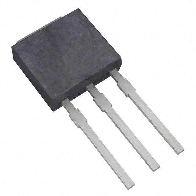
| 供应商器件封装 | D-Pak |
| 其它名称 | 497-7979-2 |
| 功率-最大值 | 95W |
| 包装 | 带卷 (TR) |
| 安装类型 | 表面贴装 |
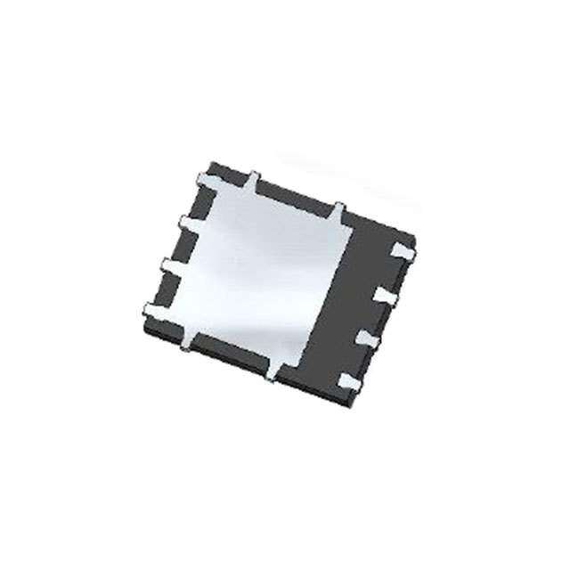
| 封装/外壳 | TO-252-3,DPak(2 引线+接片),SC-63 |
| 标准包装 | 2,500 |
| 漏源极电压(Vdss) | 30V |
| 电流-连续漏极(Id)(25°C时) | 80A (Tc) |


PDF Datasheet 数据手册内容提取
STD90N03L STD90N03L-1 Ω N-channel 30V - 0.005 - 80A - DPAK/IPAK STripFET™ III Power MOSFET General features Type V R I DSS DS(on) D STD90N03L 30V 0.0057Ω 80A (1) s ) STD90N03L-1 30V 0.0057Ω 80A (1) ( 3 ct 3 1. Pulse width limited by safe operating area 2 u 1 1 ■ R *Q industry’s benchmark d DS(on) g o ■ Conduction losses reduced r IPAK P DPAK ■ Switching losses reduced e ■ Low threshold device t e l o Description s b This device utilizes the latest advanced design O rules of ST’s proprietary STripFET™ technology. - Internal schematic diagram This is suitable for the most demanding DC-)DC s converter application where high efficiency is to ( be achieved. ct u d Applications o r P ■ Switching applications e t e l o s b O Order codes Part number Marking Package Packaging STD90N03L D90N03L DPAK Tape & reel STD90N03L-1 D90N03L-1 IPAK Tube October 2006 Rev1 1/16 www.st.com 16
Content STD90N03L - STD90N03L-1 Content 1 Electrical ratings . . . . . . . . . . . . . . . . . . . . . . . . . . . . . . . . . . . . . . . . . . . . 3 2 Electrical characteristics . . . . . . . . . . . . . . . . . . . . . . . . . . . . . . . . . . . . . 4 2.1 Electrical characteristics (curves) . . . . . . . . . . . . . . . . . . . . . . . . . . . . . 6 3 Test circuit . . . . . . . . . . . . . . . . . . . . . . . . . . . . . . . . . . . . . . . . . . . . . . . . 8 ) s 4 Package mechanical data . . . . . . . . . . . . . . . . . . . . . . . . . . . . . . . (. . . . . 11 t c u d 5 Packaging mechanical data . . . . . . . . . . . . . . . . . . . . . . . . . . . . . . . . . . 14 o r P 6 Revision history . . . . . . . . . . . . . . . . . . . . . . . . . . . . . . . . . . . . . . . . . . . 15 e t e l o s b O - ) s ( t c u d o r P e t e l o s b O 2/16
STD90N03L - STD90N03L-1 Electrical ratings 1 Electrical ratings Table 1. Absolute maximum ratings Symbol Parameter Value Unit V Drain-source voltage (V = 0) 30 V DS GS V Gate-source voltage ±20 V GS I (1) Drain current (continuous) at T = 25°C 80 A D C I Drain current (continuous) at T =100°C 64 A D C ) I (2) Drain current (pulsed) 320 sA DM ( t P Total dissipation at T = 25°C 95 c W TOT C u Derating factor 0.63 d W/°C o E (3) Single pulse avalanche energy 35r0 mJ AS P TJ Operating junction temperature e -55 to 175 °C T Storage temperature t stg e l 1. Value limited by wire bonding o s 2. Pulse width limited by safe operating area b 3. Starting Tj = 25°C, ID =40A, VDD =15V O - Table 2. Thermal data ) s ( Symbol t Parameter Value Unit c u R Thermal resistance junction-case max 1.58 °C/W thj-case d R Tohermal resistance junction-ambient max 100 °C/W thj-amb r P Maximum lead temperature for soldering e Tj purpose 275 °C t e l o s b O 3/16
Electrical characteristics STD90N03L - STD90N03L-1 2 Electrical characteristics (T =25°C unless otherwise specified) CASE Table 3. On/off states Symbol Parameter Test conditions Min. Typ. Max. Unit V(BR)DSS Dvorlataing-esource breakdown ID = 250µA, VGS= 0 30 V Zero gate voltage drain VDS = 30V 1 µA I DSS current (VGS = 0) VDS = 30V, Tc=125°C 10 s )µA ( Gate body leakage current ct IGSS (V = 0) VGS = ±20V u ±100 nA DS d VGS(th) Gate threshold voltage VDS= VGS, ID = 250µA 1 o V r P Static drain-source on VGS= 10V, ID= 40A 0.005 0.0057 Ω R DS(on) resistance V = 5V, I = 40A e 0.007 0.0011 Ω GS D t e l o Table 4. Dynamic s b Symbol Parameter O Test conditions Min. Typ. Max. Unit Ciss IOnuptuptu ct acpaapcaitcaitnacneces ) - VDS =25V, f=1MHz, 2805 pF CCorssss Rcaepvaecrsitea ntrcaenscfetr ( VGS=0 57469 ppFF u Qg Totoal gdate charge VDD=15V, ID = 80A 22 32 nC Qgs rGate-source charge VGS =5V 10 nC P Q gd Gate-drain charge (see Figure 13) 7 nC e t f=1MHz Gate Bias e Bias=0 Test Signal ol RG Gate input resistance Level=20mV 1.2 Ω s b open drain O Table 5. Switching times Symbol Parameter Test conditions Min. Typ. Max. Unit V =15V, I =40A, td(on) Turn-on delay time RDD=4.7Ω, VD =5V 19 ns t Rise time G GS 135 ns r (see Figure 12) V =15V, I =40A, td(off) Turn-off delay time RDD=4.7Ω, VD =5V 24 ns t Fall time G GS 33 ns f (see Figure 12) 4/16
STD90N03L - STD90N03L-1 Electrical characteristics Table 6. Source drain diode Symbol Parameter Test conditions Min. Typ. Max. Unit ISD Source-drain current 80 A Source-drain current I (1) 320 A SDM (pulsed) VSD(2) Forward on voltage ISD=40A, VGS=0 1.3 V trr Reverse recovery time ISD=80A, di/dt = 100A/µs, 36 ns Qrr Reverse recovery charge VDD=19 V, Tj= 150°C 32 µC I Reverse recovery current (see Figure 15) 1.8 A RRM ) s 1. Pulse width limited by safe operating area ( t 2. Pulsed: pulse duration=300µs, duty cycle 1.5% c u d o r P e t e l o s b O - ) s ( t c u d o r P e t e l o s b O 5/16
Electrical characteristics STD90N03L - STD90N03L-1 2.1 Electrical characteristics (curves) Figure 1. Safe operating area Figure 2. Thermal impedance ) s ( t c u d o r P e Figure 3. Output characteristics Figure 4. Transfer characteristics t e l o s b O - ) s ( t c u d o r P e t e l o s Fbigure 5. Static drain-source on resistance Figure 6. Normalized B vs temperature VDSS O 6/16
STD90N03L - STD90N03L-1 Electrical characteristics Figure 7. Gate charge vs gate-source voltage Figure 8. Capacitance variations ) s ( t c u d o r Figure 9. Normalized gate threshold voltage Figure 10. NormlaizedP on resistance vs vs temperature temper ature e t e l o s b O - ) s ( t c u d o r P e t e Figureo 1l1. Source-drain diode forward s characteristics b O 7/16
Test circuit STD90N03L - STD90N03L-1 3 Test circuit Figure 12. Switching times test circuit for Figure 13. Gate charge test circuit resistive load ) s ( t c u d o r P e t Figure 14. Test circuit for inductive load Figure 15. Uenclamped Inductive load test l switching and diode recovery times o circuit s b O - ) s ( t c u d o r P e t e l o s b O 8/16
STD90N03L - STD90N03L-1 Appendix A Figure 16. Buck Converter: Power Losses Estimation ) s ( t c u d o r P e The power losses associated with the FETs in a Synchtronous Buck converter can be e estimated using the equations shown in the table blelow. The formulas give a good o approximation, for the sake of performance comparison, of how different pairs of devices s affect the converter efficiency. However a vebry important parameter, the working temperature, is not considered. The reaOl device behavior is really dependent on how the heat generated inside the devices is removed to allow for a safer working junction - temperature. ) s The low side (SW2) device( requires: t c ■ Very low RDS(on)u to reduce conduction losses d ■ Small Qgls to reduce the gate charge losses o ■ Small Cross to reduce losses due to output capacitance P ■ Sm all Qrr to reduce losses on SW1 during its turn-on e e■tThe Cgd/Cgs ratio lower than Vth/Vgg ratio especially with low drain to source l o ■ voltage to avoid the cross conduction phenomenon; s b The high side (SW1) device requires: O ■ Small Rg and Ls to allow higher gate current peak and to limit the voltage feedback on the gate ■ Small Qg to have a faster commutation and to reduce gate charge losses ■ Low R to reduce the conduction losses. DS(on) 9/16
STD90N03L - STD90N03L-1 Table 7. Power losses calculation High Side Switching (SW1) Low Side Switch (SW2) Pconduction R * I2 *δ R * I2 *(1−δ) DS(on)SW1 L DS(on)SW2 L I Pswitching V *(Q +Q )*f* L Zero voltage switching in gsth(SW1) gd(SW1) I g Recovery Not applicable ) (1) V *Q *f s in rr(SW2) ( P t diode c u Conduction Not applicable d V *I *t *f f(SWo2) L deadtime r P Pgate(QG) Q *V *f e Q *V *f g(SW1) gg t gls(SW2) gg e l o s PQoss Vin*Qoss(SW1b)*f Vin*Qoss(SW2)*f O 2 2 - 1. Dissipated by SW1 during turn-on ) s Table 8. Paramiters mean(ing t c Parameter u Meaning d d o Duty-cycle r QgsthP Post threshold gate charge e Qgls Third quadrant gate charge t e ol Pconduction On state losses b s Pswitching On-off transition losses O Pdiode Conduction and reverse recovery diode losses Pgate Gate drive losses PQoss Output capacitance losses 10/16
STD90N03L - STD90N03L-1 Package mechanical data 4 Package mechanical data In order to meet environmental requirements, ST offers these devices in ECOPACK® packages. These packages have a Lead-free second level interconnect . The category of second level interconnect is marked on the package and on the inner box label, in compliance with JEDEC Standard JESD97. The maximum ratings related to soldering conditions are also marked on the inner box label. ECOPACK is an ST trademark. ECOPACK specifications are available at: www.st.com ) s ( t c u d o r P e t e l o s b O - ) s ( t c u d o r P e t e l o s b O 11/16
Package mechanical data STD90N03L - STD90N03L-1 TO-251 (IPAK) MECHANICAL DATA mm inch DIM. MIN. TYP. MAX. MIN. TYP. MAX. A 2.2 2.4 0.086 0.094 A1 0.9 1.1 0.035 0.043 A3 0.7 1.3 0.027 0.051 ) B 0.64 0.9 0.025 0.03s1 ( B2 5.2 5.4 0.204 t0.212 c B3 0.85 u 0.033 B5 0.3 0.01d2 o B6 0.95 0.037 r C 0.45 0.6 0.017 P 0.023 C2 0.48 0.6 0.01 9 0.023 e D 6 6.2 t0.236 0.244 e E 6.4 6.6 0.252 0.260 l o G 4.4 4.6 0.173 0.181 s H 15.9 b 16.3 0.626 0.641 L 9 O 9.4 0.354 0.370 L1 0.8 1.2 0.031 0.047 - L2 0.8 1 0.031 0.039 ) s ( t c u H d o C r P A t e C2 A3 e ol A1 s b L2 D L O B3 B6 B B5 3 E = B2 = 2 G = = = = 1 L1 0068771-E 12/16
STD90N03L - STD90N03L-1 Package mechanical data DPAK MECHANICAL DATA mm. inch DIM. MIN. TYP MAX. MIN. TYP. MAX. A 2.2 2.4 0.086 0.094 A1 0.9 1.1 0.035 0.043 A2 0.03 0.23 0.001 0.009 B 0.64 0.9 0.025 0.035 ) s b4 5.2 5.4 0.204 0.212 ( C 0.45 0.6 0.017 0t.023 c C2 0.48 0.6 0.019 0.023 u D 6 6.2 0.236 0.244 d D1 5.1 0.200 o E 6.4 6.6 0.252 0.260 r E1 4.7 P 0.185 e 2.28 0.090 e e1 4.4 4.6 0.173 0.181 t H 9.35 10.1 e 0.368 0.397 L 1 l 0.039 o (L1) 2.8 0.110 s L2 0.8 0.031 b L4 0.6 O 1 0.023 0.039 R 0.2 0.008 V2 0° - 8° 0° 8° ) s ( t c u d o r P e t e l o s b O 0068772-F 13/16
Packaging mechanical data STD90N03L - STD90N03L-1 5 Packaging mechanical data DPAK FOOTPRINT ) s ( t c All dimensions are in millimeters u d o r P TAPE AND REEL SHIPMENT e t ReEEL MECHANICAL DATA l o mm inch DIM. s MIN. MAX. MIN. MAX. b A 330 12.992 O B 1.5 0.059 - C 12.8 13.2 0.504 0.520 ) s D 20.2 0.795 ( G 16.4 18.4 0.645 0.724 t c N 50 1.968 u T 22.4 0.881 d o BASE QTY BULK QTY TAPE MErCHANICAL DATA P 2500 2500 mm inch DIM. e MIN. MAX. MIN. MAX. t e A0 6.8 7 0.267 0.275 ol B0 10.4 10.6 0.409 0.417 s B1 12.1 0.476 b D 1.5 1.6 0.059 0.063 O D1 1.5 0.059 E 1.65 1.85 0.065 0.073 F 7.4 7.6 0.291 0.299 K0 2.55 2.75 0.100 0.108 P0 3.9 4.1 0.153 0.161 P1 7.9 8.1 0.311 0.319 P2 1.9 2.1 0.075 0.082 R 40 1.574 W 15.7 16.3 0.618 0.641 14/16
STD90N03L - STD90N03L-1 Revision history 6 Revision history T able 9. Revision history Date Revision Changes 20-Oct-2006 1 Initial release. ) s ( t c u d o r P e t e l o s b O - ) s ( t c u d o r P e t e l o s b O 15/16
Revision history STD90N03L - STD90N03L-1 ) s ( t Please Read Carefully: c u d Information in this document is provided solely in connection with ST products. STMicroelectronics NV and itso subsidiaries (“ST”) reserve the right to make changes, corrections, modifications or improvements, to this document, and the products arnd services described herein at any P time, without notice. e All ST products are sold pursuant to ST’s terms and conditions of sale. t e Purchasers are solely responsible for the choice, selection and use of the ST products and services described herein, and ST assumes no l liability whatsoever relating to the choice, selection or use of the ST products and soervices described herein. s No license, express or implied, by estoppel or otherwise, to any intellectual property rights is granted under this document. If any part of this b document refers to any third party products or services it shall not be deemed a license grant by ST for the use of such third party products O or services, or any intellectual property contained therein or considered as a warranty covering the use in any manner whatsoever of such third party products or services or any intellectual property con-tai ned therein. ) s UNLESS OTHERWISE SET FORTH IN ST’S TE(RMS AND CONDITIONS OF SALE ST DISCLAIMS ANY EXPRESS OR IMPLIED t WARRANTY WITH RESPECT TO THE USEc AND/OR SALE OF ST PRODUCTS INCLUDING WITHOUT LIMITATION IMPLIED WARRANTIES OF MERCHANTABILITY, FuITNESS FOR A PARTICULAR PURPOSE (AND THEIR EQUIVALENTS UNDER THE LAWS OF ANY JURISDICTION), OR INFRINGdEMENT OF ANY PATENT, COPYRIGHT OR OTHER INTELLECTUAL PROPERTY RIGHT. o UNLESS EXPRESSLY APPROVED IN WRITING BY AN AUTHORIZED ST REPRESENTATIVE, ST PRODUCTS ARE NOT r RECOMMENDED, AUTHORPIZED OR WARRANTED FOR USE IN MILITARY, AIR CRAFT, SPACE, LIFE SAVING, OR LIFE SUSTAINING APPLICATIONS, NOR IN PRODUCTS OR SYSTEMS WHERE FAILURE OR MALFUNCTION MAY RESULT IN PERSONAL INJURY, e DEATH, OR SEVERE PROPERTY OR ENVIRONMENTAL DAMAGE. ST PRODUCTS WHICH ARE NOT SPECIFIED AS "AUTOMOTIVE t GRADE" MAY eONLY BE USED IN AUTOMOTIVE APPLICATIONS AT USER’S OWN RISK. l o s Resale of ST products with provisions different from the statements and/or technical features set forth in this document shall immediately void b any warranty granted by ST for the ST product or service described herein and shall not create or extend in any manner whatsoever, any O liability of ST. ST and the ST logo are trademarks or registered trademarks of ST in various countries. Information in this document supersedes and replaces all information previously supplied. The ST logo is a registered trademark of STMicroelectronics. All other names are the property of their respective owners. © 2006 STMicroelectronics - All rights reserved STMicroelectronics group of companies Australia - Belgium - Brazil - Canada - China - Czech Republic - Finland - France - Germany - Hong Kong - India - Israel - Italy - Japan - Malaysia - Malta - Morocco - Singapore - Spain - Sweden - Switzerland - United Kingdom - United States of America www.st.com 16/16