ICGOO在线商城 > 分立半导体产品 > 晶体管 - FET,MOSFET - 单 > STB11NK40ZT4
 Datasheet下载
- 型号: STB11NK40ZT4
- 制造商: STMicroelectronics
- 库位|库存: xxxx|xxxx
- 要求:
| 数量阶梯 | 香港交货 | 国内含税 |
| +xxxx | $xxxx | ¥xxxx |
查看当月历史价格
查看今年历史价格
STB11NK40ZT4产品简介:
ICGOO电子元器件商城为您提供STB11NK40ZT4由STMicroelectronics设计生产,在icgoo商城现货销售,并且可以通过原厂、代理商等渠道进行代购。 STB11NK40ZT4价格参考。STMicroelectronicsSTB11NK40ZT4封装/规格:晶体管 - FET,MOSFET - 单, 表面贴装 N 沟道 400V 9A(Tc) 110W(Tc) D2PAK。您可以下载STB11NK40ZT4参考资料、Datasheet数据手册功能说明书,资料中有STB11NK40ZT4 详细功能的应用电路图电压和使用方法及教程。
STMicroelectronics的STB11NK40ZT4是一款N沟道增强型MOSFET,广泛应用于需要高效功率开关的场景。其主要应用场景包括:

1. 电源管理:适用于开关电源(SMPS)、DC-DC转换器和电源适配器,实现高效的能量转换和稳定的电压调节。

2. 电机控制:用于直流电机驱动、步进电机控制等场合,提供快速开关响应和良好的导通性能。

3. 照明系统:如LED驱动器和工业照明设备中,作为功率开关元件,支持调光和节能功能。

4. 工业自动化:在工业控制系统中,用于继电器替代、负载开关和保护电路,提升系统可靠性和寿命。

5. 消费电子:常见于家电(如变频空调、洗衣机)和高功率充电设备中,实现高效能与小型化设计。

6. 汽车电子:用于车载电源系统、电动助力转向(EPS)和电池管理系统(BMS),满足汽车环境下的高可靠性和耐温要求。

该器件具有低导通电阻、高耐压(400V)和强电流能力(11A),适合高频开关应用,同时具备良好的热稳定性和抗干扰能力,适用于多种中高功率电子系统。
| 参数 | 数值 |
| 产品目录 | |
| ChannelMode | Enhancement |
| 描述 | MOSFET N-CH 400V 9A D2PAKMOSFET N-Ch 400 Volt 9 Amp Zener SuperMESH |
| 产品分类 | FET - 单分离式半导体 |
| FET功能 | 标准 |
| FET类型 | MOSFET N 通道,金属氧化物 |
| Id-ContinuousDrainCurrent | 9 A |
| Id-连续漏极电流 | 9 A |
| 品牌 | STMicroelectronics |
| 产品手册 | |
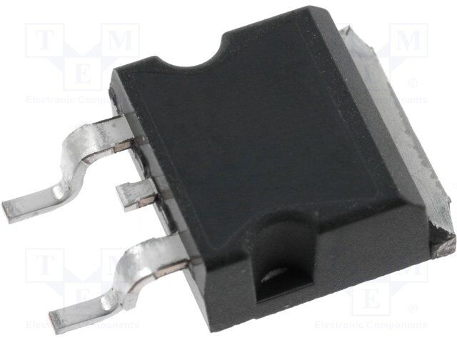
| 产品图片 |
|
| rohs | 符合RoHS无铅 / 符合限制有害物质指令(RoHS)规范要求 |
| 产品系列 | 晶体管,MOSFET,STMicroelectronics STB11NK40ZT4SuperMESH™ |
| 数据手册 | |
| 产品型号 | STB11NK40ZT4 |
| Pd-PowerDissipation | 110 W |
| Pd-功率耗散 | 110 W |
| RdsOn-Drain-SourceResistance | 550 mOhms |
| RdsOn-漏源导通电阻 | 550 mOhms |
| Vds-Drain-SourceBreakdownVoltage | 400 V |
| Vds-漏源极击穿电压 | 400 V |
| Vgs-Gate-SourceBreakdownVoltage | +/- 30 V |
| Vgs-栅源极击穿电压 | 30 V |
| 上升时间 | 20 ns |
| 下降时间 | 18 ns |
| 不同Id时的Vgs(th)(最大值) | 4.5V @ 100µA |
| 不同Vds时的输入电容(Ciss) | 930pF @ 25V |
| 不同Vgs时的栅极电荷(Qg) | 32nC @ 10V |
| 不同 Id、Vgs时的 RdsOn(最大值) | 550 毫欧 @ 4.5A,10V |
| 产品目录页面 | |
| 产品种类 | MOSFET |
| 供应商器件封装 | D2PAK |
| 其它名称 | 497-7930-1 |
| 其它有关文件 | http://www.st.com/web/catalog/sense_power/FM100/CL824/SC1166/PF67094?referrer=70071840 |
| 典型关闭延迟时间 | 40 ns |
| 功率-最大值 | 110W |
| 包装 | 剪切带 (CT) |
| 商标 | STMicroelectronics |
| 安装类型 | 表面贴装 |
| 安装风格 | SMD/SMT |
| 封装 | Reel |
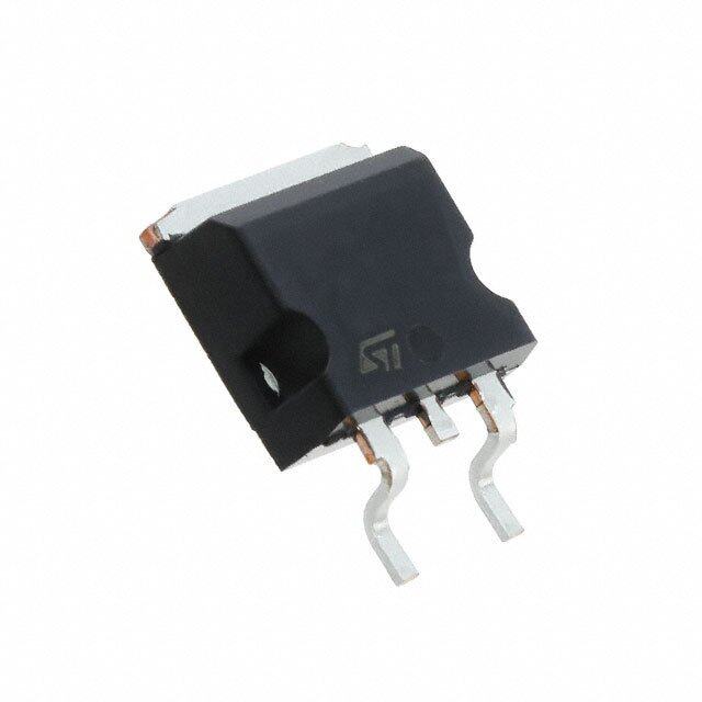
| 封装/外壳 | TO-263-3,D²Pak(2 引线+接片),TO-263AB |
| 封装/箱体 | D2PAK-2 |
| 工厂包装数量 | 1000 |
| 晶体管极性 | N-Channel |
| 最大工作温度 | + 150 C |
| 最小工作温度 | - 55 C |
| 标准包装 | 1 |
| 正向跨导-最小值 | 5.8 S |
| 漏源极电压(Vdss) | 400V |
| 电流-连续漏极(Id)(25°C时) | 9A (Tc) |
| 系列 | STB11NK40Z |
| 通道模式 | Enhancement |
| 配置 | Single |


- 商务部:美国ITC正式对集成电路等产品启动337调查
- 曝三星4nm工艺存在良率问题 高通将骁龙8 Gen1或转产台积电
- 太阳诱电将投资9.5亿元在常州建新厂生产MLCC 预计2023年完工
- 英特尔发布欧洲新工厂建设计划 深化IDM 2.0 战略
- 台积电先进制程称霸业界 有大客户加持明年业绩稳了
- 达到5530亿美元!SIA预计今年全球半导体销售额将创下新高
- 英特尔拟将自动驾驶子公司Mobileye上市 估值或超500亿美元
- 三星加码芯片和SET,合并消费电子和移动部门,撤换高东真等 CEO
- 三星电子宣布重大人事变动 还合并消费电子和移动部门
- 海关总署:前11个月进口集成电路产品价值2.52万亿元 增长14.8%


PDF Datasheet 数据手册内容提取
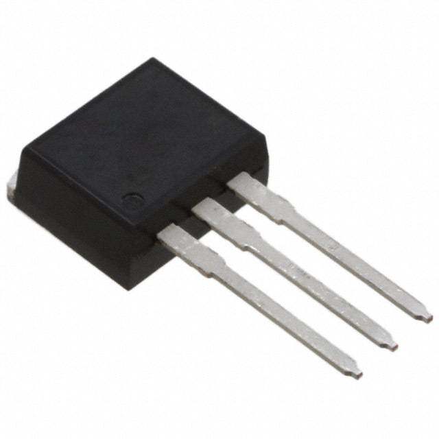
STB11NK40Z, STP11NK40ZFP STP11NK40Z Ω 2 N-channel 400 V, 0.49 , 9 A, TO-220, TO-220FP, D PAK TM Zener-protected SuperMESH Power MOSFET Features Type V R I Pw DSS DS(on) D STB11NK40Z 400V <0.55Ω 10A 110W STP11NK40Z 400V <0.55Ω 10A 110W 3 23 2 1 1 STP11NK40ZFP 400V <0.55Ω 10A 30W TO-220 TO-220FP ■ Extremely high dv/dt capability ■ 100% avalanche tested 3 1 ■ Gate charge minimized D2PAK ■ Very low intrinsic capacitances ■ Very good manufacturing repeatability Applications ■ Switching application Figure 1. Internal schematic diagram Description The SuperMESH™ series is obtained through an extreme optimization of ST’s well established strip-based PowerMESH™ layout. In addition to pushing on-resistance significantly down, special care is taken to ensure a very good dv/dt capability for the most demanding applications. Table 1. Device summary Order code Marking Package Packaging STB11NK40ZT4 B11NK40Z D²PAK Tape and reel STP11NK40Z P11NK40Z TO-220 Tube STP11NK40ZFP P11NK40ZFP TO-220FP Tube April 2009 Doc ID 8936 Rev 7 1/17 www.st.com 17
Contents STB11NK40Z, STP11NK40ZFP, STP11NK40Z Contents 1 Electrical ratings . . . . . . . . . . . . . . . . . . . . . . . . . . . . . . . . . . . . . . . . . . . . 3 2 Electrical characteristics . . . . . . . . . . . . . . . . . . . . . . . . . . . . . . . . . . . . . 5 2.1 Electrical characteristics (curves) . . . . . . . . . . . . . . . . . . . . . . . . . . . . 7 3 Test circuits . . . . . . . . . . . . . . . . . . . . . . . . . . . . . . . . . . . . . . . . . . . . . 10 4 Package mechanical data . . . . . . . . . . . . . . . . . . . . . . . . . . . . . . . . . . . . 11 5 Packaging mechanical data . . . . . . . . . . . . . . . . . . . . . . . . . . . . . . . . . . 15 6 Revision history . . . . . . . . . . . . . . . . . . . . . . . . . . . . . . . . . . . . . . . . . . . 16 2/17 Doc ID 8936 Rev 7
STB11NK40Z, STP11NK40ZFP, STP11NK40Z Electrical ratings 1 Electrical ratings Table 2. Absolute maximum ratings Value Symbol Parameter Unit TO-220/D²PAK TO-220FP V Drain-source voltage (V = 0) 400 V DS GS V Drain-gate voltage (R = 20KΩ) 400 V DGR GS V Gate-source voltage ± 30 V GS I Drain current (continuous) at T = 25°C 9 9(1) A D C I Drain current (continuous) at T =100°C 5.67 5.67(1) A D C I (2) Drain current (pulsed) 36 36(1) A DM P Total dissipation at T = 25°C 110 30 W TOT C Derating factor 0.88 0.24 W/°C Gate source ESD (HBM-C= 100pF, V 3500 V ESD(G-S) R= 1.5kΩ) dv/dt(3) Peak diode recovery voltage slope 4.5 V/ns V Insulation withstand voltage (DC) -- 2500 V ISO T Operating junction temperature J -55 to 150 °C T Storage temperature stg 1. Limited only by maximum temperature allowed 2. Pulse width limited by safe operating area 3. I ≤ 9A, di/dt ≤ 200 A/µs, V ≤ V , T ≤ T SD DD (BR)DSS j JMAX. Table 3. Thermal data Value Symbol Parameter Unit TO-220/D²PAK TO-220FP R Thermal resistance junction-case max 1.14 4.2 °C/W thj-case R Thermal resistance junction-ambient max 62.5 °C/W thj-a Maximum lead temperature for soldering T 300 °C l purpose Doc ID 8936 Rev 7 3/17
Electrical ratings STB11NK40Z, STP11NK40ZFP, STP11NK40Z Table 4. Avalanche characteristics Symbol Parameter Value Unit Avalanche current, repetitive or not- I 9 A AR repetitive (pulse width limited by T max) j Single pulse avalanche energy E 190 mJ AS (starting T=25°C, Id=Iar, Vdd=50V) j 4/17 Doc ID 8936 Rev 7
STB11NK40Z, STP11NK40ZFP, STP11NK40Z Electrical characteristics 2 Electrical characteristics (T =25°C unless otherwise specified) CASE Table 5. On/off states Symbol Parameter Test conditions Min. Typ. Max. Unit Drain-source breakdown V(BR)DSS voltage ID = 1mA, VGS= 0 400 V Zero gate voltage drain VDS = Max rating, 1 µA I DSS current (VGS = 0) VDS = Max rating @125°C 50 µA Gate body leakage current IGSS (V = 0) VGS = ± 20V, VDS = 0 ±10 µA DS VGS(th) Gate threshold voltage VDS= VGS, ID = 100µA 3 3.75 4.5 V Static drain-source on RDS(on) resistance VGS= 10V, ID= 4.5A 0.49 0.55 Ω Table 6. Dynamic Symbol Parameter Test conditions Min. Typ. Max. Unit gfs (1) Forward transconductance VDS =15V, ID = 4.5A - 5.8 - S C Input capacitance iss 930 pF C Output capacitance oss VDS =25V, f=1 MHz, VGS=0 - 140 - pF Reverse transfer Crss 30 pF capacitance Coss eq(2). Ecaqpuaivcaitlaennct eoutput VGS=0, VDS =0V to 320V - 78 - pF Qg Total gate charge VDD=320V, ID = 9A 32 nC Qgs Gate-source charge VGS =10V - 6 - nC Qgd Gate-drain charge (see Figure 18) 18.5 nC 1. Pulsed: pulse duration=300µs, duty cycle 1.5% 2. C is defined as a constant equivalent capacitance giving the same charging time as C when V oss eq. oss DS inceases from 0 to 80% V DSS Doc ID 8936 Rev 7 5/17
Electrical characteristics STB11NK40Z, STP11NK40ZFP, STP11NK40Z Table 7. Switching times Symbol Parameter Test conditions Min. Typ. Max. Unit V =200 V, I =4.5A, td(on) Turn-on delay time RDD=4.7Ω, VD=10V - 20 - ns t Rise time G GS 20 ns r (see Figure 20) V =200V, I =4.5A, td(off) Turn-off delay time RDD=4.7Ω, VD =10V - 40 - ns t Fall time G GS 18 ns f (see Figure 20) tr(Voff) Off-voltage rise time VDD=320V, ID=9A, 15 ns tf Fall time RG=4.7Ω, VGS=10V - 17 - ns tc Cross-over time (see Figure 20) 30 ns Table 8. Source drain diode Symbol Parameter Test conditions Min. Typ. Max Unit ISD Source-drain current - 9 A I (1) Source-drain current (pulsed) - 36 A SDM VSD(2) Forward on voltage ISD=9A, VGS=0 - 1.6 V trr Reverse recovery time ISD=9A, 225 ns Qrr Reverse recovery charge di/dt = 100A/µs, - 1.6 µC IRRM Reverse recovery current VDD=45V, Tj=150°C 14 A 1. Pulse width limited by safe operating area 2. Pulsed: pulse duration=300 µs, duty cycle 1.5 % Table 9. Gate-source zener diode Symbol Parameter Test conditions Min. Typ. Max. Unit BVGSO Gate-source breakdown voltage Igs=±1mA (open drain) 30 - - V The built-in back-to-back Zener diodes have specifically been designed to enhance not only the device’s ESD capability, but also to make them safely absorb possible voltage transients that may occasionally be applied from gate to source. In this respect the Zener voltage is appropriate to achieve an efficient and cost-effective intervention to protect the device’s integrity. These integrated Zener diodes thus avoid the usage of external components. 6/17 Doc ID 8936 Rev 7
STB11NK40Z, STP11NK40ZFP, STP11NK40Z Electrical characteristics 2.1 Electrical characteristics (curves) Figure 2. Safe operating area for TO-220 Figure 3. Thermal impedance for TO-220 D²PAK D²PAK Figure 4. Safe operating area for TO-220FP Figure 5. Thermal impedance for TO-220FP Figure 6. Output characteristics Figure 7. Transfer characteristics Doc ID 8936 Rev 7 7/17
Electrical characteristics STB11NK40Z, STP11NK40ZFP, STP11NK40Z Figure 8. Transconductance Figure 9. Static drain-source on resistance Figure 10. Gate charge vs gate-source voltage Figure 11. Capacitance variations Figure 12. Normalized gate threshold voltage Figure 13. Normalized on resistance vs vs temperature temperature 8/17 Doc ID 8936 Rev 7
STB11NK40Z, STP11NK40ZFP, STP11NK40Z Electrical characteristics Figure 14. Source-drain diode forward Figure 15. Normalized B vs temperature VDSS characteristics Figure 16. Maximum avalanche energy vs temperature Doc ID 8936 Rev 7 9/17
Test circuits STB11NK40Z, STP11NK40ZFP, STP11NK40Z 3 Test circuits Figure 17. Switching times test circuit for Figure 18. Gate charge test circuit resistive load Figure 19. Test circuit for inductive load Figure 20. Unclamped inductive load test switching and diode recovery times circuit Figure 21. Unclamped inductive waveform Figure 22. Switching time waveform 10/17 Doc ID 8936 Rev 7
STB11NK40Z, STP11NK40ZFP, STP11NK40Z Package mechanical data 4 Package mechanical data In order to meet environmental requirements, ST offers these devices in different grades of ECOPACK® packages, depending on their level of environmental compliance. ECOPACK® specifications, grade definitions and product status are available at: www.st.com. ECOPACK is an ST trademark. Doc ID 8936 Rev 7 11/17
Package mechanical data STB11NK40Z, STP11NK40ZFP, STP11NK40Z D²PAK (TO-263) mechanical data mm inch Dim Min Typ Max Min Typ Max A 4.40 4.60 0.173 0.181 A1 0.03 0.23 0.001 0.009 b 0.70 0.93 0.027 0.037 b2 1.14 1.70 0.045 0.067 c 0.45 0.60 0.017 0.024 c2 1.23 1.36 0.048 0.053 D 8.95 9.35 0.352 0.368 D1 7.50 0.295 E 10 10.40 0.394 0.409 E1 8.50 0.334 e 2.54 0.1 e1 4.88 5.28 0.192 0.208 H 15 15.85 0.590 0.624 J1 2.49 2.69 0.099 0.106 L 2.29 2.79 0.090 0.110 L1 1.27 1.40 0.05 0.055 L2 1.30 1.75 0.051 0.069 R 0.4 0.016 V2 0° 8° 0° 8° 0079457_M 12/17 Doc ID 8936 Rev 7
STB11NK40Z, STP11NK40ZFP, STP11NK40Z Package mechanical data TO-220 mechanical data mm inch Dim Min Typ Max Min Typ Max A 4.40 4.60 0.173 0.181 b 0.61 0.88 0.024 0.034 b1 1.14 1.70 0.044 0.066 c 0.48 0.70 0.019 0.027 D 15.25 15.75 0.6 0.62 D1 1.27 0.050 E 10 10.40 0.393 0.409 e 2.40 2.70 0.094 0.106 e1 4.95 5.15 0.194 0.202 F 1.23 1.32 0.048 0.051 H1 6.20 6.60 0.244 0.256 J1 2.40 2.72 0.094 0.107 L 13 14 0.511 0.551 L1 3.50 3.93 0.137 0.154 L20 16.40 0.645 L30 28.90 1.137 ∅P 3.75 3.85 0.147 0.151 Q 2.65 2.95 0.104 0.116 Doc ID 8936 Rev 7 13/17
Package mechanical data STB11NK40Z, STP11NK40ZFP, STP11NK40Z TO-220FP mechanical data mm Dim. Min. Typ. Max. A 4.4 4.6 B 2.5 2.7 D 2.5 2.75 E 0.45 0.7 F 0.75 1 F1 1.15 1.70 F2 1.15 1.5 G 4.95 5.2 G1 2.4 2.7 H 10 10.4 L2 16 L3 28.6 30.6 L4 9.8 10.6 L5 2.9 3.6 L6 15.9 16.4 L7 9 9.3 Dia 3 3.2 L7 E A B D Dia L5 L6 F1 F2 F H G G1 L2 L4 L3 7012510_Rev_J 14/17 Doc ID 8936 Rev 7
STB11NK40Z, STP11NK40ZFP, STP11NK40Z Packaging mechanical data 5 Packaging mechanical data D2PAK FOOTPRINT TAPE AND REEL SHIPMENT REEL MECHANICAL DATA mm inch DIM. MIN. MAX. MIN. MAX. A 330 12.992 B 1.5 0.059 C 12.8 13.2 0.504 0.520 D 20.2 0795 G 24.4 26.4 0.960 1.039 N 100 3.937 T 30.4 1.197 BASE QTY BULK QTY TAPE MECHANICAL DATA 1000 1000 mm inch DIM. MIN. MAX. MIN. MAX. A0 10.5 10.7 0.413 0.421 B0 15.7 15.9 0.618 0.626 D 1.5 1.6 0.059 0.063 D1 1.59 1.61 0.062 0.063 E 1.65 1.85 0.065 0.073 F 11.4 11.6 0.449 0.456 K0 4.8 5.0 0.189 0.197 P0 3.9 4.1 0.153 0.161 P1 11.9 12.1 0.468 0.476 P2 1.9 2.1 0.075 0.082 R 50 1.574 T 0.25 0.35 0.0098 0.0137 W 23.7 24.3 0.933 0.956 * on sales type Doc ID 8936 Rev 7 15/17
Revision history STB11NK40Z, STP11NK40ZFP, STP11NK40Z 6 Revision history T able 10. Document revision history Date Revision Changes 23-Aug-2005 2 Preliminary version 28-Oct-2005 3 Complete version 26-Jul-2006 4 New template, no content change 22-Nov-2006 5 Corrected unit on Table 5.: On/off states 18-Jan-2007 6 Typo mistakes on page 1 20-Apr-2009 7 Updated mechanical data 16/17 Doc ID 8936 Rev 7
STB11NK40Z, STP11NK40ZFP, STP11NK40Z Please Read Carefully: Information in this document is provided solely in connection with ST products. STMicroelectronics NV and its subsidiaries (“ST”) reserve the right to make changes, corrections, modifications or improvements, to this document, and the products and services described herein at any time, without notice. All ST products are sold pursuant to ST’s terms and conditions of sale. Purchasers are solely responsible for the choice, selection and use of the ST products and services described herein, and ST assumes no liability whatsoever relating to the choice, selection or use of the ST products and services described herein. No license, express or implied, by estoppel or otherwise, to any intellectual property rights is granted under this document. If any part of this document refers to any third party products or services it shall not be deemed a license grant by ST for the use of such third party products or services, or any intellectual property contained therein or considered as a warranty covering the use in any manner whatsoever of such third party products or services or any intellectual property contained therein. UNLESS OTHERWISE SET FORTH IN ST’S TERMS AND CONDITIONS OF SALE ST DISCLAIMS ANY EXPRESS OR IMPLIED WARRANTY WITH RESPECT TO THE USE AND/OR SALE OF ST PRODUCTS INCLUDING WITHOUT LIMITATION IMPLIED WARRANTIES OF MERCHANTABILITY, FITNESS FOR A PARTICULAR PURPOSE (AND THEIR EQUIVALENTS UNDER THE LAWS OF ANY JURISDICTION), OR INFRINGEMENT OF ANY PATENT, COPYRIGHT OR OTHER INTELLECTUAL PROPERTY RIGHT. UNLESS EXPRESSLY APPROVED IN WRITING BY AN AUTHORIZED ST REPRESENTATIVE, ST PRODUCTS ARE NOT RECOMMENDED, AUTHORIZED OR WARRANTED FOR USE IN MILITARY, AIR CRAFT, SPACE, LIFE SAVING, OR LIFE SUSTAINING APPLICATIONS, NOR IN PRODUCTS OR SYSTEMS WHERE FAILURE OR MALFUNCTION MAY RESULT IN PERSONAL INJURY, DEATH, OR SEVERE PROPERTY OR ENVIRONMENTAL DAMAGE. ST PRODUCTS WHICH ARE NOT SPECIFIED AS "AUTOMOTIVE GRADE" MAY ONLY BE USED IN AUTOMOTIVE APPLICATIONS AT USER’S OWN RISK. Resale of ST products with provisions different from the statements and/or technical features set forth in this document shall immediately void any warranty granted by ST for the ST product or service described herein and shall not create or extend in any manner whatsoever, any liability of ST. ST and the ST logo are trademarks or registered trademarks of ST in various countries. Information in this document supersedes and replaces all information previously supplied. The ST logo is a registered trademark of STMicroelectronics. All other names are the property of their respective owners. © 2009 STMicroelectronics - All rights reserved STMicroelectronics group of companies Australia - Belgium - Brazil - Canada - China - Czech Republic - Finland - France - Germany - Hong Kong - India - Israel - Italy - Japan - Malaysia - Malta - Morocco - Philippines - Singapore - Spain - Sweden - Switzerland - United Kingdom - United States of America www.st.com Doc ID 8936 Rev 7 17/17
Mouser Electronics Authorized Distributor Click to View Pricing, Inventory, Delivery & Lifecycle Information: S TMicroelectronics: STP11NK40Z STP11NK40ZFP STB11NK40ZT4