ICGOO在线商城 > 分立半导体产品 > 晶体管 - FET,MOSFET - 单 > SIHF15N60E-E3
 Datasheet下载
- 型号: SIHF15N60E-E3
- 制造商: Vishay
- 库位|库存: xxxx|xxxx
- 要求:
| 数量阶梯 | 香港交货 | 国内含税 |
| +xxxx | $xxxx | ¥xxxx |
查看当月历史价格
查看今年历史价格
SIHF15N60E-E3产品简介:
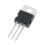
ICGOO电子元器件商城为您提供SIHF15N60E-E3由Vishay设计生产,在icgoo商城现货销售,并且可以通过原厂、代理商等渠道进行代购。 SIHF15N60E-E3价格参考¥12.39-¥12.39。VishaySIHF15N60E-E3封装/规格:晶体管 - FET,MOSFET - 单, 通孔 N 沟道 600V 15A(Tc) 34W(Tc) TO-220 整包。您可以下载SIHF15N60E-E3参考资料、Datasheet数据手册功能说明书,资料中有SIHF15N60E-E3 详细功能的应用电路图电压和使用方法及教程。
Vishay Siliconix 的 SIHF15N60E-E3 是一款 N 沟道增强型功率 MOSFET,具有15A电流承载能力和600V漏源击穿电压。该器件广泛应用于需要高效能和高可靠性的电源管理系统中。

其主要应用场景包括:

1. 电源适配器与充电器:适用于笔记本电脑、手机等电子设备的AC-DC电源转换器,提供高效的能量转换。
2. 工业电源系统:如不间断电源(UPS)、开关电源(SMPS)及变频器,用于提高能源效率和减小体积。
3. 电机控制与驱动电路:在电动工具、家用电器或自动化设备中,用于直流电机或步进电机的驱动控制。
4. 照明系统:如LED照明驱动电源,支持高效率和稳定输出。
5. 新能源应用:例如太阳能逆变器、储能系统中的DC-DC转换模块,利用其高耐压和低导通电阻特性提升整体效率。

SIHF15N60E-E3具备低RDS(on)、快速开关特性和高耐用性,适合高频工作环境,有助于减少发热并提高系统稳定性。
| 参数 | 数值 |
| 产品目录 | |
| 描述 | MOSFET N-CH 600V 15A TO220 FULLPMOSFET 600V 280mOhm@10V 15A N-Ch E-SRS |
| 产品分类 | FET - 单分离式半导体 |
| FET功能 | 标准 |
| FET类型 | MOSFET N 通道,金属氧化物 |
| Id-ContinuousDrainCurrent | 15 A |
| Id-连续漏极电流 | 15 A |
| 品牌 | Vishay / SiliconixVishay Siliconix |
| 产品手册 | |
| 产品图片 |
|
| rohs | 符合RoHS无铅 / 符合限制有害物质指令(RoHS)规范要求 |
| 产品系列 | 晶体管,MOSFET,Vishay / Siliconix SIHF15N60E-E3- |
| 数据手册 | |
| 产品型号 | SIHF15N60E-E3SIHF15N60E-E3 |
| Pd-PowerDissipation | 180 W |
| Pd-功率耗散 | 180 W |
| Qg-GateCharge | 38 nC |
| Qg-栅极电荷 | 38 nC |
| RdsOn-Drain-SourceResistance | 280 mOhms |
| RdsOn-漏源导通电阻 | 280 mOhms |
| Vds-Drain-SourceBreakdownVoltage | 600 V |
| Vds-漏源极击穿电压 | 600 V |
| Vgs-Gate-SourceBreakdownVoltage | +/- 20 V |
| Vgs-栅源极击穿电压 | 20 V |
| 上升时间 | 51 nS |
| 下降时间 | 33 nS |
| 不同Id时的Vgs(th)(最大值) | 4V @ 250µA |
| 不同Vds时的输入电容(Ciss) | 1350pF @ 100V |
| 不同Vgs时的栅极电荷(Qg) | 78nC @ 10V |
| 不同 Id、Vgs时的 RdsOn(最大值) | 280 毫欧 @ 8A,10V |
| 产品培训模块 | http://www.digikey.cn/PTM/IndividualPTM.page?site=cn&lang=zhs&ptm=30391 |
| 产品种类 | MOSFET |
| 供应商器件封装 | TO-220 整包 |
| 其它名称 | SIHF15N60EE3 |
| 典型关闭延迟时间 | 35 nS |
| 功率-最大值 | 34W |
| 包装 | 散装 |
| 商标 | Vishay / Siliconix |
| 安装类型 | 通孔 |
| 安装风格 | Through Hole |
| 导通电阻 | 280 mOhms |
| 封装 | Tube |
| 封装/外壳 | TO-220-3 整包 |
| 封装/箱体 | TO-220FP-3 |
| 工厂包装数量 | 50 |
| 晶体管极性 | N-Channel |
| 最大工作温度 | + 150 C |
| 最小工作温度 | - 55 C |
| 标准包装 | 1,000 |
| 正向跨导-最小值 | 4.6 S |
| 汲极/源极击穿电压 | 600 V |
| 漏极连续电流 | 15 A |
| 漏源极电压(Vdss) | 600V |
| 电流-连续漏极(Id)(25°C时) | 15A (Tc) |
| 系列 | E |
| 配置 | Single |


- 商务部:美国ITC正式对集成电路等产品启动337调查
- 曝三星4nm工艺存在良率问题 高通将骁龙8 Gen1或转产台积电
- 太阳诱电将投资9.5亿元在常州建新厂生产MLCC 预计2023年完工
- 英特尔发布欧洲新工厂建设计划 深化IDM 2.0 战略
- 台积电先进制程称霸业界 有大客户加持明年业绩稳了
- 达到5530亿美元!SIA预计今年全球半导体销售额将创下新高
- 英特尔拟将自动驾驶子公司Mobileye上市 估值或超500亿美元
- 三星加码芯片和SET,合并消费电子和移动部门,撤换高东真等 CEO
- 三星电子宣布重大人事变动 还合并消费电子和移动部门
- 海关总署:前11个月进口集成电路产品价值2.52万亿元 增长14.8%


PDF Datasheet 数据手册内容提取
SiHF15N60E www.vishay.com Vishay Siliconix E Series Power MOSFET FEATURES D TO-220 FULLPAK • Low figure-of-merit (FOM) R x Q on g • Low input capacitance (C ) iss • Reduced switching and conduction losses G • Ultra low gate charge (Q ) g Available • Avalanche energy rated (UIS) • Material categorization: for definitions of compliance S please see www.vishay.com/doc?99912 G D S N-Channel MOSFET APPLICATIONS • Server and telecom power supplies PRODUCT SUMMARY • Switch mode power supplies (SMPS) V (V) at T max. 650 • Power factor correction power supplies (PFC) DS J RDS(on) max. () at 25 °C VGS = 10 V 0.28 • Lighting Q max. (nC) 78 - High-intensity discharge (HID) g Q (nC) 9 - Fluorescent ballast lighting gs Q (nC) 17 • Industrial gd Configuration Single - Welding - Induction heating - Motor drives - Battery chargers - Renewable energy - Solar (PV inverters) ORDERING INFORMATION Package TO-220 FULLPAK Lead (Pb)-free SiHF15N60E-E3 Lead (Pb)-free and Halogen-free SiHF15N60E-GE3 ABSOLUTE MAXIMUM RATINGS (T = 25 °C, unless otherwise noted) C PARAMETER SYMBOL LIMIT UNIT Drain-Source Voltage V 600 DS V Gate-Source Voltage V ± 30 GS T = 25 °C 15 Continuous Drain Current (T = 150 °C) e V at 10 V C I J GS D T = 100 °C 9.6 A C Pulsed Drain Current a I 39 DM Linear Derating Factor 0.27 W/°C Single Pulse Avalanche Energy b E 102 mJ AS Maximum Power Dissipation P 34 W D Operating Junction and Storage Temperature Range T , T -55 to +150 °C J stg Drain-Source Voltage Slope V = 0 V to 80 % V 70 DS DS dV/dt V/ns Reverse Diode dV/dt d 7.7 Soldering Recommendations (Peak temperature) c For 10 s 300 °C Mounting Torque M3 screw 0.6 Nm Notes a. Repetitive rating; pulse width limited by maximum junction temperature. b. VDD = 50 V, starting TJ = 25 °C, L = 11.6 mH, Rg = 25 , IAS = 4.2 A. c. 1.6 mm from case. d. ISD ID, dI/dt = 100 A/μs, starting TJ = 25 °C. e. Limited by maximum junction temperature. S16-1602-Rev. I, 15-Aug-16 1 Document Number: 91480 For technical questions, contact: hvm@vishay.com THIS DOCUMENT IS SUBJECT TO CHANGE WITHOUT NOTICE. THE PRODUCTS DESCRIBED HEREIN AND THIS DOCUMENT ARE SUBJECT TO SPECIFIC DISCLAIMERS, SET FORTH AT www.vishay.com/doc?91000
SiHF15N60E www.vishay.com Vishay Siliconix THERMAL RESISTANCE RATINGS PARAMETER SYMBOL TYP. MAX. UNIT Maximum Junction-to-Ambient R - 65 thJA °C/W Maximum Junction-to-Case (Drain) R - 3.7 thJC SPECIFICATIONS (T = 25 °C, unless otherwise noted) J PARAMETER SYMBOL TEST CONDITIONS MIN. TYP. MAX. UNIT Static Drain-Source Breakdown Voltage V V = 0 V, I = 250 μA 600 - - V DS GS D VDS Temperature Coefficient VDS/TJ Reference to 25 °C, ID = 1 mA - 0.71 - V/°C Gate-Source Threshold Voltage (N) V V = V , I = 250 μA 2 - 4 V GS(th) DS GS D V = ± 20 V - - ± 100 nA GS Gate-Source Leakage I GSS V = ± 30 V - - ± 1 μA GS V = 600 V, V = 0 V - - 1 DS GS Zero Gate Voltage Drain Current I μA DSS V = 480 V, V = 0 V, T = 125 °C - - 10 DS GS J Drain-Source On-State Resistance RDS(on) VGS = 10 V ID = 8 A - 0.23 0.28 Forward Transconductance g V = 30 V, I = 8 A - 4.6 - S fs DS D Dynamic Input Capacitance C - 1350 - iss V = 0 V, GS Output Capacitance C V = 100 V, - 70 - oss DS f = 1 MHz Reverse Transfer Capacitance C - 5 - rss pF Effective Output Capacitance, Energy C - 53 - Related a o(er) V = 0 V to 480 V, V = 0 V DS GS Effective Output Capacitance, Time C - 177 - Related b o(tr) Total Gate Charge Q - 39 78 g Gate-Source Charge Q V = 10 V I = 8 A, V = 480 V - 11 - nC gs GS D DS Gate-Drain Charge Q - 17 - gd Turn-On Delay Time t - 16 32 d(on) Rise Time t - 26 52 r VDD = 480 V, ID = 8 A, ns Turn-Off Delay Time td(off) VGS = 10 V, Rg = 9.1 - 41 82 Fall Time t - 22 44 f Gate Input Resistance Rg f = 1 MHz, open drain 0.3 0.86 1.7 Drain-Source Body Diode Characteristics MOSFET symbol Continuous Source-Drain Diode Current IS showing the D - - 15 A integral reverse G Pulsed Diode Forward Current I - - 60 SM p - n junction diode S Diode Forward Voltage V T = 25 °C, I = 8 A, V = 0 V - 1.0 1.2 V SD J S GS Reverse Recovery Time t - 302 604 ns rr T = 25 °C, I = I = 8 A, Reverse Recovery Charge Q J F S - 4.0 8 μC rr dI/dt = 100 A/μs, V = 25 V R Reverse Recovery Current I - 24 - A RRM Notes a. C is a fixed capacitance that gives the same energy as C while V is rising from 0 % to 80 % V . oss(er) oss DS DSS b. C is a fixed capacitance that gives the same charging time as C while V is rising from 0 % to 80 % V . oss(tr) oss DS DSS S16-1602-Rev. I, 15-Aug-16 2 Document Number: 91480 For technical questions, contact: hvm@vishay.com THIS DOCUMENT IS SUBJECT TO CHANGE WITHOUT NOTICE. THE PRODUCTS DESCRIBED HEREIN AND THIS DOCUMENT ARE SUBJECT TO SPECIFIC DISCLAIMERS, SET FORTH AT www.vishay.com/doc?91000
SiHF15N60E www.vishay.com Vishay Siliconix TYPICAL CHARACTERISTICS (25 °C, unless otherwise noted) 50 3 TOP 15 V A) 1143 VV TJ = 25 °C ID = 8 A nt ( 40 1121 VV eed) 2.5 urce Curre 30 BOTTOM 1 059876 VVVVVV n-to-Source (Normaliz 1.25 , Drain-to-SoD 1200 R, DraiDS(on)On Resistanc 0.15 VGS = 10 V I 0 0 0 5 10 15 20 25 30 - 60- 40- 20 0 20 40 60 80 100120140160 VDS, Drain-to-Source Voltage (V) TJ, Junction Temperature (°C) Fig. 1 - Typical Output Characteristics Fig. 4 - Normalized On-Resistance vs. Temperature 30 10 000 A) TOP 111543 VVV TJ = 150 °C nt ( 25 1121 VV Ciss o-Source Curre 1250 BOTTOM 1 09876 VVVVV pacitance (pF) 1100000 Coss VCCCGirosssSsss = === 0 CCC gVgdsd,s +f+ = CC 1ggd dM, CHdzs Shorted n-t 10 Ca ai 10 Crss Dr , D 5 I 5 V 0 1 0 5 10 15 20 25 30 0 100 200 300 400 500 600 V , Drain-to-Source Voltage (V) DS V , Drain-to-Source Voltage (V) DS Fig. 2 - Typical Output Characteristics Fig. 5 - Typical Capacitance vs. Drain-to-Source Voltage 50 10 A) T = 25 °C 9 nt ( 40 J 8 urre 2000 7 C o-Source 2300 TJ = 150 °C C (pF) oss 200 Coss Eoss 456 E (μJ) oss n-t 3 ai Dr 10 2 , D I 1 0 20 0 0 5 10 15 20 25 0 100 200 300 400 500 600 VGS, Gate-to-Source Voltage (V) VDS Fig. 3 - Typical Transfer Characteristics Fig. 6 - C and E vs. V oss oss DS S16-1602-Rev. I, 15-Aug-16 3 Document Number: 91480 For technical questions, contact: hvm@vishay.com THIS DOCUMENT IS SUBJECT TO CHANGE WITHOUT NOTICE. THE PRODUCTS DESCRIBED HEREIN AND THIS DOCUMENT ARE SUBJECT TO SPECIFIC DISCLAIMERS, SET FORTH AT www.vishay.com/doc?91000
SiHF15N60E www.vishay.com Vishay Siliconix 24 20 V = 480 V ge (V) 20 VVDDDSSS == 310200 VV e Volta 16 ent (A) 15 ourc 12 Curr 10 o-S ain ate-t 8 , DrD 5 G I , S 4 G V 0 0 0 20 40 60 80 25 50 75 100 125 150 Qg, Total Gate Charge (nC) TJ, Case Temperature (°C) Fig. 7 - Typical Gate Charge vs. Gate-to-Source Voltage Fig. 10 - Maximum Drain Current vs. Case Temperature 100 750 A) 725 se Drain Current ( 10 TJ = 150 °C TJ = 25 °C Drain-to-Sourcedown Voltage (V) 666725705050 Rever 1 V, DSBreak 567050 , D IS V = 0 V 550 GS 0.1 525 0.2 0.4 0.6 0.8 1 1.2 1.4 1.6 - 60- 40- 20 0 20 40 60 80 100120140160 V , Source-Drain Voltage (V) T , Junction Temperature (°C) SD J Fig. 8 - Typical Source-Drain Diode Forward Voltage Fig. 11 - Temperature vs. Drain-to-Source Voltage 100 Operation in this Area Limited by RDS(on) IDMLimited 10 A) 100 μs ent ( Limited by RDS(on)* Curr 1 n ai 1 ms Dr , D I 0.1 10 ms T = 25 °C C T = 150 °C J Single Pulse BVDSS Limited 0.01 1 10 100 1000 V , Drain-to-Source Voltage (V) DS * V > minimum V at which R is specified GS GS DS(on) Fig. 9 - Maximum Safe Operating Area S16-1602-Rev. I, 15-Aug-16 4 Document Number: 91480 For technical questions, contact: hvm@vishay.com THIS DOCUMENT IS SUBJECT TO CHANGE WITHOUT NOTICE. THE PRODUCTS DESCRIBED HEREIN AND THIS DOCUMENT ARE SUBJECT TO SPECIFIC DISCLAIMERS, SET FORTH AT www.vishay.com/doc?91000
SiHF15N60E www.vishay.com Vishay Siliconix 1 Duty Cycle = 0.5 nt sie 0.2 ective Tranmpedance 0.1 0.1 d Effmal I 0.020.05 alizeTher Single Pulse m or N 0.01 0.0001 0.001 0.01 0.1 1 10 Pulse Time (s) Fig. 12 - Normalized Thermal Transient Impedance, Junction-to-Case RD VDS V DS t p VGS D.U.T. VDD R G + -VDD V DS 10 V Pulse width ≤ 1 µs Duty factor ≤ 0.1 % I AS Fig. 13 - Switching Time Test Circuit Fig. 16 - Unclamped Inductive Waveforms V DS Q G 90 % 10 V Q Q GS GD 10 % V G V GS t t t t d(on) r d(off) f Charge Fig. 14 - Switching Time Waveforms Fig. 17 - Basic Gate Charge Waveform L Current regulator V Same type as D.U.T. DS Vary t to obtain p required IAS 50 kΩ RG D.U.T + 12 V 0.2 µF 0.3 µF V - DD + I V AS D.U.T. - DS 10 V tp 0.01 Ω VGS 3 mA Fig. 15 - Unclamped Inductive Test Circuit I I G D Current sampling resistors Fig. 18 - Gate Charge Test Circuit S16-1602-Rev. I, 15-Aug-16 5 Document Number: 91480 For technical questions, contact: hvm@vishay.com THIS DOCUMENT IS SUBJECT TO CHANGE WITHOUT NOTICE. THE PRODUCTS DESCRIBED HEREIN AND THIS DOCUMENT ARE SUBJECT TO SPECIFIC DISCLAIMERS, SET FORTH AT www.vishay.com/doc?91000
SiHF15N60E www.vishay.com Vishay Siliconix Peak Diode Recovery dV/dt Test Circuit + Circuit layout considerations D.U.T. (cid:129) Low stray inductance (cid:129) Ground plane (cid:129) Low leakage inductance current transformer - + - + - Rg (cid:129) dV/dt controlled by Rg + (cid:129) Driver same type as D.U.T. V - DD (cid:129) ISD controlled by duty factor “D” (cid:129) D.U.T. - device under test Driver gate drive Period D = P.W. P.W. Period V = 10 Va GS D.U.T. l waveform SD Reverse recovery Body diode forward current current dI/dt D.U.T. V waveform DS Diode recovery dV/dt V DD Re-applied voltage Body diode forward drop Inductor current Ripple ≤ 5 % ISD Note a. V = 5 V for logic level devices GS Fig. 19 - For N-Channel Vishay Siliconix maintains worldwide manufacturing capability. Products may be manufactured at one of several qualified locations. Reliability data for Silicon Technology and Package Reliability represent a composite of all qualified locations. For related documents such as package/tape drawings, part marking, and reliability data, see www.vishay.com/ppg?91480. S16-1602-Rev. I, 15-Aug-16 6 Document Number: 91480 For technical questions, contact: hvm@vishay.com THIS DOCUMENT IS SUBJECT TO CHANGE WITHOUT NOTICE. THE PRODUCTS DESCRIBED HEREIN AND THIS DOCUMENT ARE SUBJECT TO SPECIFIC DISCLAIMERS, SET FORTH AT www.vishay.com/doc?91000
Package Information Vishay Siliconix TO-220 FULLPAK (HIGH VOLTAGE) E A Ø P A1 n d1 d3 D u L1 V L b3 A2 b2 c b e MILLIMETERS INCHES DIM. MIN. MAX. MIN. MAX. A 4.570 4.830 0.180 0.190 A1 2.570 2.830 0.101 0.111 A2 2.510 2.850 0.099 0.112 b 0.622 0.890 0.024 0.035 b2 1.229 1.400 0.048 0.055 b3 1.229 1.400 0.048 0.055 c 0.440 0.629 0.017 0.025 D 8.650 9.800 0.341 0.386 d1 15.88 16.120 0.622 0.635 d3 12.300 12.920 0.484 0.509 E 10.360 10.630 0.408 0.419 e 2.54 BSC 0.100 BSC L 13.200 13.730 0.520 0.541 L1 3.100 3.500 0.122 0.138 n 6.050 6.150 0.238 0.242 Ø P 3.050 3.450 0.120 0.136 u 2.400 2.500 0.094 0.098 v 0.400 0.500 0.016 0.020 ECN: X09-0126-Rev. B, 26-Oct-09 DWG: 5972 Notes 1. To be used only for process drawing. 2. These dimensions apply to all TO-220, FULLPAK leadframe versions 3 leads. 3. All critical dimensions should C meet C > 1.33. pk 4. All dimensions include burrs and plating thickness. 5. No chipping or package damage. Document Number: 91359 www.vishay.com Revision: 26-Oct-09 1
Legal Disclaimer Notice www.vishay.com Vishay Disclaimer ALL PRODUCT, PRODUCT SPECIFICATIONS AND DATA ARE SUBJECT TO CHANGE WITHOUT NOTICE TO IMPROVE RELIABILITY, FUNCTION OR DESIGN OR OTHERWISE. Vishay Intertechnology, Inc., its affiliates, agents, and employees, and all persons acting on its or their behalf (collectively, “Vishay”), disclaim any and all liability for any errors, inaccuracies or incompleteness contained in any datasheet or in any other disclosure relating to any product. Vishay makes no warranty, representation or guarantee regarding the suitability of the products for any particular purpose or the continuing production of any product. To the maximum extent permitted by applicable law, Vishay disclaims (i) any and all liability arising out of the application or use of any product, (ii) any and all liability, including without limitation special, consequential or incidental damages, and (iii) any and all implied warranties, including warranties of fitness for particular purpose, non-infringement and merchantability. Statements regarding the suitability of products for certain types of applications are based on Vishay’s knowledge of typical requirements that are often placed on Vishay products in generic applications. Such statements are not binding statements about the suitability of products for a particular application. It is the customer’s responsibility to validate that a particular product with the properties described in the product specification is suitable for use in a particular application. Parameters provided in datasheets and / or specifications may vary in different applications and performance may vary over time. All operating parameters, including typical parameters, must be validated for each customer application by the customer’s technical experts. Product specifications do not expand or otherwise modify Vishay’s terms and conditions of purchase, including but not limited to the warranty expressed therein. Except as expressly indicated in writing, Vishay products are not designed for use in medical, life-saving, or life-sustaining applications or for any other application in which the failure of the Vishay product could result in personal injury or death. Customers using or selling Vishay products not expressly indicated for use in such applications do so at their own risk. Please contact authorized Vishay personnel to obtain written terms and conditions regarding products designed for such applications. No license, express or implied, by estoppel or otherwise, to any intellectual property rights is granted by this document or by any conduct of Vishay. Product names and markings noted herein may be trademarks of their respective owners. © 2017 VISHAY INTERTECHNOLOGY, INC. ALL RIGHTS RESERVED Revision: 08-Feb-17 1 Document Number: 91000
Mouser Electronics Authorized Distributor Click to View Pricing, Inventory, Delivery & Lifecycle Information: V ishay: SIHF15N60E-E3 SIHF15N60E-GE3