ICGOO在线商城 > 分立半导体产品 > 晶体管 - FET,MOSFET - 单 > STW78N65M5
 Datasheet下载
- 型号: STW78N65M5
- 制造商: STMicroelectronics
- 库位|库存: xxxx|xxxx
- 要求:
| 数量阶梯 | 香港交货 | 国内含税 |
| +xxxx | $xxxx | ¥xxxx |
查看当月历史价格
查看今年历史价格
STW78N65M5产品简介:
ICGOO电子元器件商城为您提供STW78N65M5由STMicroelectronics设计生产,在icgoo商城现货销售,并且可以通过原厂、代理商等渠道进行代购。 STW78N65M5价格参考。STMicroelectronicsSTW78N65M5封装/规格:晶体管 - FET,MOSFET - 单, 通孔 N 沟道 650V 69A(Tc) 450W(Tc) TO-247。您可以下载STW78N65M5参考资料、Datasheet数据手册功能说明书,资料中有STW78N65M5 详细功能的应用电路图电压和使用方法及教程。
STMicroelectronics的型号STW78N65M5是一款N沟道增强型MOSFET,其主要应用场景包括但不限于以下几个方面:

1. 开关电源(SMPS):该MOSFET适用于各种开关模式电源设计,如AC-DC转换器、DC-DC转换器和反激式转换器。它能够高效地处理高电压输入,并在高频开关条件下保持较低的导通电阻(Rds(on)),从而减少功率损耗。

2. 电机驱动:由于其高耐压(650V)和低导通电阻特性,STW78N65M5非常适合用于工业电机控制、家用电器中的电机驱动以及电动工具的电源管理。它可以承受电机启动时的大电流冲击,并提供稳定的运行性能。

3. 逆变器:在太阳能逆变器或不间断电源(UPS)系统中,这款MOSFET可以作为关键组件来实现高效的电能转换与管理。其快速开关能力和良好的热稳定性有助于提高整体效率并延长设备寿命。

4. PFC电路(功率因数校正):在需要进行功率因数校正的应用场合,例如大型家电、服务器电源等,STW78N65M5可被用作主开关器件之一,帮助优化输入电流波形以满足电磁兼容性要求。

5. 负载切换与保护:在汽车电子、通信基站等领域,该产品可用于实现负载的动态切换及过流保护功能。凭借其坚固耐用的设计和出色的电气参数,能够在严苛环境下可靠工作。

总之,STW78N65M5凭借其优异的电气特性和可靠性,广泛应用于消费类电子产品、工业自动化设备以及新能源技术等多个领域,为各类电力电子系统提供了高性能解决方案。
| 参数 | 数值 |
| 产品目录 | |
| 描述 | MOSF N CH 650V 69A TO247MOSFET N-Ch 650 V 0.033 Ohm 69 A MDmesh(TM) |
| 产品分类 | FET - 单分离式半导体 |
| FET功能 | 标准 |
| FET类型 | MOSFET N 通道,金属氧化物 |
| Id-连续漏极电流 | 69 A |
| 品牌 | STMicroelectronics |
| 产品手册 | |
| 产品图片 |
|
| rohs | 符合RoHS无铅 / 符合限制有害物质指令(RoHS)规范要求 |
| 产品系列 | 晶体管,MOSFET,STMicroelectronics STW78N65M5MDmesh™ V |
| 数据手册 | |
| 产品型号 | STW78N65M5 |
| Pd-PowerDissipation | 450 W |
| Pd-功率耗散 | 450 W |
| Qg-GateCharge | 203 nC |
| Qg-栅极电荷 | 203 nC |
| RdsOn-漏源导通电阻 | 24 mOhms |
| Vds-漏源极击穿电压 | 650 V |
| Vgs-Gate-SourceBreakdownVoltage | 25 V |
| Vgs-栅源极击穿电压 | 25 V |
| Vgsth-Gate-SourceThresholdVoltage | 4 V |
| Vgsth-栅源极阈值电压 | 4 V |
| 上升时间 | 14 ns |
| 下降时间 | 14 ns |
| 不同Id时的Vgs(th)(最大值) | 5V @ 250µA |
| 不同Vds时的输入电容(Ciss) | 9000pF @ 100V |
| 不同Vgs时的栅极电荷(Qg) | 203nC @ 10V |
| 不同 Id、Vgs时的 RdsOn(最大值) | 32 毫欧 @ 34.5A, 10V |
| 产品种类 | MOSFET |
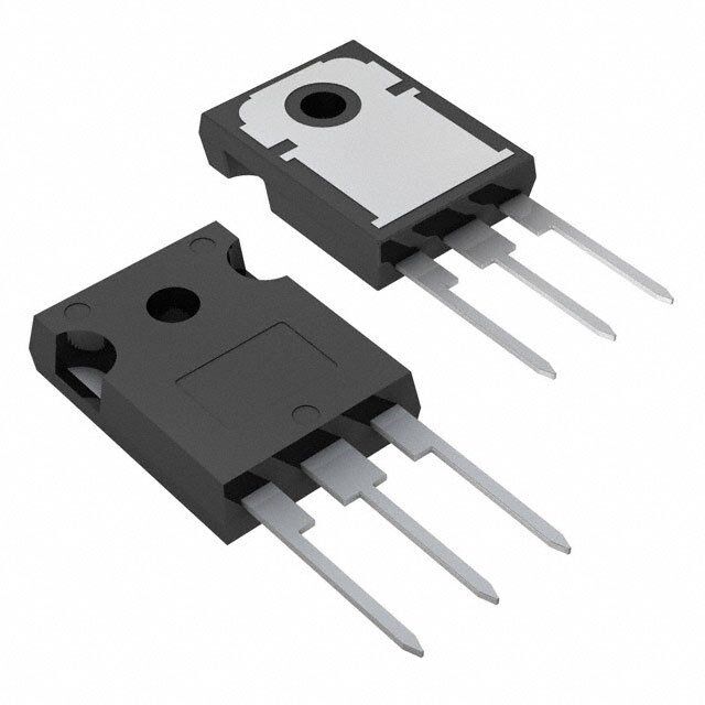
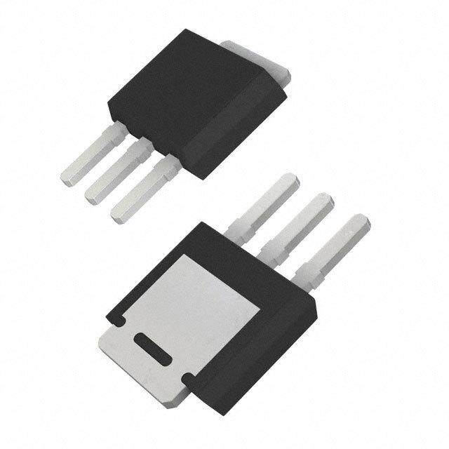
| 供应商器件封装 | TO-247 |
| 其它名称 | 497-13603-5 |
| 其它有关文件 | http://www.st.com/web/catalog/sense_power/FM100/CL824/SC1167/PF253746?referrer=70071840 |
| 功率-最大值 | 450W |
| 包装 | 管件 |
| 商标 | STMicroelectronics |
| 商标名 | MDmesh |
| 安装类型 | 通孔 |
| 安装风格 | Through Hole |
| 导通电阻 | 24 mOhms |
| 封装 | Tube |
| 封装/外壳 | TO-247-3 |
| 封装/箱体 | TO-247-3 |
| 工厂包装数量 | 30 |
| 晶体管极性 | N-Channel |
| 最大工作温度 | + 150 C |
| 最小工作温度 | - 55 C |
| 标准包装 | 30 |
| 汲极/源极击穿电压 | 650 V |
| 漏极连续电流 | 69 A |
| 漏源极电压(Vdss) | 650V |
| 电流-连续漏极(Id)(25°C时) | 69A (Tc) |
| 系列 | STW78N65M5 |
| 通道模式 | Enhancement |
| 配置 | Single |


- 商务部:美国ITC正式对集成电路等产品启动337调查
- 曝三星4nm工艺存在良率问题 高通将骁龙8 Gen1或转产台积电
- 太阳诱电将投资9.5亿元在常州建新厂生产MLCC 预计2023年完工
- 英特尔发布欧洲新工厂建设计划 深化IDM 2.0 战略
- 台积电先进制程称霸业界 有大客户加持明年业绩稳了
- 达到5530亿美元!SIA预计今年全球半导体销售额将创下新高
- 英特尔拟将自动驾驶子公司Mobileye上市 估值或超500亿美元
- 三星加码芯片和SET,合并消费电子和移动部门,撤换高东真等 CEO
- 三星电子宣布重大人事变动 还合并消费电子和移动部门
- 海关总署:前11个月进口集成电路产品价值2.52万亿元 增长14.8%


PDF Datasheet 数据手册内容提取
STW78N65M5 Ω Automotive-grade N-channel 650 V, 0.024 typ., 69 A, MDmesh™ V Power MOSFET in a TO-247 package Datasheet - production data Features Order code V @T R max. I DS jmax. DS(on) D STW78N65M5 710 V 0.032 Ω 69 A • Designed for automotive applications and AEC-Q101 qualified 3 2 • Higher V rating 1 DSS • Higher dv/dt capability TO-247 • Excellent switching performance • Easy to drive • 100% avalanche tested Figure 1. Internal schematic diagram Applications • Switching applications (cid:39)(cid:11)(cid:21)(cid:12) Description This device is an N-channel MDmesh™ V Power MOSFET based on an innovative proprietary (cid:42)(cid:11)(cid:20)(cid:12) vertical process technology, which is combined with STMicroelectronics’ well-known PowerMESH™ horizontal layout structure. The (cid:54)(cid:11)(cid:22)(cid:12) resulting product has extremely low on- resistance, which is unmatched among silicon- based Power MOSFETs, making it especially (cid:36)(cid:48)(cid:19)(cid:20)(cid:23)(cid:26)(cid:24)(cid:89)(cid:20) suitable for applications which require superior power density and outstanding efficiency. Table 1. Device summary Order code Marking Package Packaging STW78N65M5 78N65M5 TO-247 Tube August 2013 DocID023457 Rev 4 1/14 This is information on a product in full production. www.st.com
Contents STW78N65M5 Contents 1 Electrical ratings . . . . . . . . . . . . . . . . . . . . . . . . . . . . . . . . . . . . . . . . . . . . 3 2 Electrical characteristics . . . . . . . . . . . . . . . . . . . . . . . . . . . . . . . . . . . . . 4 2.1 Electrical characteristics (curves) . . . . . . . . . . . . . . . . . . . . . . . . . . . . 6 3 Test circuits . . . . . . . . . . . . . . . . . . . . . . . . . . . . . . . . . . . . . . . . . . . . . . 9 4 Package mechanical data . . . . . . . . . . . . . . . . . . . . . . . . . . . . . . . . . . . . 10 5 Revision history . . . . . . . . . . . . . . . . . . . . . . . . . . . . . . . . . . . . . . . . . . . 13 2/14 DocID023457 Rev 4
STW78N65M5 Electrical ratings 1 Electrical ratings Table 2. Absolute maximum ratings Symbol Parameter Value Unit V Gate- source voltage ±25 V GS I Drain current (continuous) at T = 25 °C 69 A D C I Drain current (continuous) at T = 100 °C 41.5 A D C I (1) Drain current (pulsed) 276 A DM P Total dissipation at T = 25 °C 450 W TOT C dv/dt (2) Peak diode recovery voltage slope 15 V/ns dv/dt (3) MOSFET dv/dt ruggedness 50 V/ns T Storage temperature - 55 to 150 °C stg T Max. operating junction temperature 150 °C j 1. Pulse width limited by safe operating area 2. I ≤ 69 A, di/dt = 400 A/µs, V < V , V = 400 V SD DS peak (BR)DSS DD 3. V ≤ 520 V DS Table 3. Thermal data Symbol Parameter Value Unit R Thermal resistance junction-case max 0.28 °C/W thj-case R Thermal resistance junction-ambient max 50 °C/W thj-amb Table 4. Avalanche characteristics Symbol Parameter Value Unit Max current during repetitive or single pulse avalanche I 15 A AR (pulse width limited by T ) JMAX Single pulse avalanche energy E 2000 mJ AS (starting T = 25 °C, I = I , V = 50 V) j D AR DD DocID023457 Rev 4 3/14 14
Electrical characteristics STW78N65M5 2 Electrical characteristics (T = 25 °C unless otherwise specified) C Table 5. On /off states Symbol Parameter Test conditions Min. Typ. Max. Unit Drain-source V breakdown voltage I = 1 mA 650 V (BR)DSS D (V = 0) GS Zero gate voltage V = 650 V 1 µA I DS DSS drain current (V = 0) V = 650 V, T =125 °C 100 µA GS DS C Gate-body leakage I V = ± 25 V ±100 nA GSS current (V = 0) GS DS V Gate threshold voltage V = V , I = 250 µA 3 4 5 V GS(th) DS GS D Static drain-source on- R V = 10 V, I = 34.5 A 0.024 0.032 Ω DS(on) resistance GS D Table 6. Dynamic Symbol Parameter Test conditions Min. Typ. Max. Unit C Input capacitance - 9000 - pF iss Coss Output capacitance VDS = 100 V, f = 1 MHz, - 210 - pF V = 0 Reverse transfer GS C - 9 - pF rss capacitance Equivalent C (1) capacitance time V = 0, V = 0 to 520 V - 768 - pF o(tr) GS DS related Equivalent C (2) capacitance energy V = 0, V = 0 to 520 V - 205 - pF o(er) GS DS related Intrinsic gate R f = 1 MHz open drain - 1.5 - Ω G resistance Q Total gate charge - 203 - nC g V = 520 V, I = 34.5 A, DD D Q Gate-source charge V = 10 V - 50 - nC gs GS (see Figure16) Q Gate-drain charge - 84 - nC gd 1. C is a constant capacitance value that gives the same charging time as C while V is rising from 0 o(tr) oss DS to 80% V . DSS 2. C is a constant capacitance value that gives the same stored energy as C while V is rising from 0 o(er) oss DS to 80% V . DSS 4/14 DocID023457 Rev 4
STW78N65M5 Electrical characteristics Table 7. Switching times Symbol Parameter Test conditions Min. Typ. Max. Unit t Voltage delay time - 163 - ns d(V) V = 400 V, I = 40 A, DD D tr(V) Voltage rise time RG = 4.7 Ω, VGS = 10 V - 14 - ns t Current fall time (see Figure17) - 14 - ns f(i) (see Figure20) t Crossing time - 26 - ns c(off) Table 8. Source drain diode Symbol Parameter Test conditions Min. Typ. Max. Unit I Source-drain current - 69 A SD I (1) Source-drain current (pulsed) - 276 A SDM V (2) Forward on voltage I = 69 A, V = 0 - 1.5 V SD SD GS t Reverse recovery time - 504 ns rr I = 69 A, SD Q Reverse recovery charge di/dt = 100 A/µs - 13 µC rr V = 100 V (see Figure17) I Reverse recovery current DD - 49 A RRM t Reverse recovery time I = 69 A, - 635 ns rr SD di/dt = 100 A/µs Q Reverse recovery charge - 19 µC rr V = 100 V, T = 150 °C DD j IRRM Reverse recovery current (see Figure17) - 59 A 1. Pulse width limited by safe operating area 2. Pulsed: pulse duration = 300 µs, duty cycle 1.5% DocID023457 Rev 4 5/14 14
Electrical characteristics STW78N65M5 2.1 Electrical characteristics (curves) Figure 2. Safe operating area Figure 3. Thermal impedance ID AM15574v1 (A) 11000 OpeLriatmiitoen di nb ty hims aaxr eRa DiSs(on) 11000µµss 1ms 10ms Tj=150°C 1 Tc=25°C Single pulse 0.1 0.1 1 10 100 VDS(V) Figure 4. Output characteristics Figure 5. Transfer characteristics ID AM10393v1 ID(A) AM10394v1 (A) VDS=30V 225 250 VGS=10V 200 8V 175 200 150 150 125 7V 100 100 75 50 50 6V 25 0 0 0 5 10 15 20 25 VDS(V) 3 4 5 6 7 8 9 VGS(V) Figure 6. Gate charge vs gate-source voltage Figure 7. Static drain-source on-resistance VGS AM15575v1 RDS(on) AM10396v1 (V) (Ω) VDD=520V VGS=10V 12 ID=34.5A 0.026 10 8 0.024 6 4 0.022 2 0 0.020 0 50 100 150 200 250Qg(nC) 0 10 20 30 40 50 60 70 80 ID(A) 6/14 DocID023457 Rev 4
STW78N65M5 Electrical characteristics Figure 8. Capacitance variations Figure 9. Output capacitance stored energy C AM15577v1 Eoss AM10398v1 (pF) (µJ) 40 100000 35 10000 Ciss 30 25 1000 20 Coss 100 15 10 10 Crss 5 1 0 0.1 1 10 100 1000 VDS(V) 0 100 200 300 400 500 600 VDS(V) Figure 10. Normalized gate threshold voltage vs Figure 11. Normalized on-resistance vs temperature temperature VGS(th) AM04972v1 RDS(on) AM15573v1 (norm) (norm) 1.10 ID=250µA VDS=10 V VDS=VGS 2.5 ID=34.5 A 1.00 2 1.5 0.90 1 0.80 0.5 0.70 0 -50 -25 0 25 50 75 100 TJ(°C) -55 -25 5 35 65 95 125 TJ(°C) Figure 12. Source-drain diode forward Figure 13. Normalized V vs temperature DS characteristics VSD AM04974v1 VDS AM10399v1 (V) (norm) TJ=-50°C 1.08 1.2 ID = 1mA 1.06 1.0 1.04 0.8 1.02 TJ=25°C 1.00 0.6 TJ=150°C 0.98 0.4 0.96 0.2 0.94 0 0.92 0 10 20 30 40 50 ISD(A) -50 -25 0 25 50 75 100 TJ(°C) DocID023457 Rev 4 7/14 14
Electrical characteristics STW78N65M5 Figure 14. Switching losses vs gate resistance (1) AM15576v1 E(µJ) VDD=400V VGS=10V Eon 2500 ID=40A 2000 1500 Eoff 1000 500 0 0 10 20 30 40 RG(Ω) 1. Eon including reverse recovery of a SiC diode 8/14 DocID023457 Rev 4
STW78N65M5 Test circuits 3 Test circuits Figure 15. Switching times test circuit for Figure 16. Gate charge test circuit resistive load VDD 12V 47kΩ 1kΩ 100nF RL 2μ20F0 3μ.F3 VDD IG=CONST VD Vi=20V=VGMAX 100Ω D.U.T. VGS 2200 RG D.U.T. μF 2.7kΩ VG PW 47kΩ 1kΩ PW AM01468v1 AM01469v1 Figure 17. Test circuit for inductive load Figure 18. Unclamped inductive load test circuit switching and diode recovery times L A A A D FAST L=100μH VD G D.U.T. DIODE 2200 3.3 μF μF VDD S B 3.3 1000 B B μF μF 25Ω D VDD ID G RG S Vi D.U.T. Pw AM01470v1 AM01471v1 Figure 19. Unclamped inductive waveform Figure 20. Switching time waveform V(BR)DSS (cid:38)(cid:82)(cid:81)(cid:70)(cid:72)(cid:83)(cid:87)(cid:3)(cid:90)(cid:68)(cid:89)(cid:72)(cid:73)(cid:82)(cid:85)(cid:80)(cid:3)(cid:73)(cid:82)(cid:85)(cid:3)(cid:44)(cid:81)(cid:71)(cid:88)(cid:70)(cid:87)(cid:76)(cid:89)(cid:72)(cid:3)(cid:47)(cid:82)(cid:68)(cid:71)(cid:3)(cid:55)(cid:88)(cid:85)(cid:81)(cid:16)(cid:82)(cid:73)(cid:73)(cid:3) (cid:44)(cid:71) VD (cid:28)(cid:19)(cid:8)(cid:57)(cid:71)(cid:86) (cid:28)(cid:19)(cid:8)(cid:44)(cid:71) (cid:55)(cid:71)(cid:72)(cid:79)(cid:68)(cid:92)(cid:16)(cid:16)(cid:82)(cid:82)(cid:73)(cid:73)(cid:73)(cid:73) IDM (cid:57)(cid:74)(cid:86) (cid:28)(cid:19)(cid:8)(cid:57)(cid:74)(cid:86) (cid:82)(cid:82)(cid:81)(cid:81) ID (cid:57)(cid:74)(cid:86)(cid:11)(cid:44)(cid:11)(cid:87)(cid:12)(cid:12)(cid:12)(cid:12) VDD VDD (cid:20)(cid:19)(cid:8)(cid:57)(cid:71)(cid:86) (cid:20)(cid:19)(cid:8)(cid:44)(cid:71) (cid:57)(cid:71)(cid:86) (cid:55)(cid:55)(cid:85)(cid:85)(cid:76)(cid:76)(cid:86)(cid:86)(cid:72)(cid:72) (cid:55)(cid:55)(cid:73)(cid:73)(cid:68)(cid:68)(cid:79)(cid:79)(cid:79)(cid:79) AM01472v1 (cid:55)(cid:70)(cid:85)(cid:82)(cid:86)(cid:86)(cid:16)(cid:16)(cid:82)(cid:89)(cid:72)(cid:85) (cid:36)(cid:48)(cid:19)(cid:24)(cid:24)(cid:23)(cid:19)(cid:89)(cid:20) DocID023457 Rev 4 9/14 14
Package mechanical data STW78N65M5 4 Package mechanical data In order to meet environmental requirements, ST offers these devices in different grades of ECOPACK® packages, depending on their level of environmental compliance. ECOPACK® specifications, grade definitions and product status are available at: www.st.com. ECOPACK is an ST trademark. 10/14 DocID023457 Rev 4
STW78N65M5 Package mechanical data Table 9. TO-247 mechanical data mm. Dim. Min. Typ. Max. A 4.85 5.15 A1 2.20 2.60 b 1.0 1.40 b1 2.0 2.40 b2 3.0 3.40 c 0.40 0.80 D 19.85 20.15 E 15.45 15.75 e 5.30 5.45 5.60 L 14.20 14.80 L1 3.70 4.30 L2 18.50 ∅P 3.55 3.65 ∅R 4.50 5.50 S 5.30 5.50 5.70 DocID023457 Rev 4 11/14 14
Package mechanical data STW78N65M5 Figure 21. TO-247 drawing 0075325_G 12/14 DocID023457 Rev 4
STW78N65M5 Revision history 5 Revision history Table 10. Document revision history Date Revision Changes 16-Jul-2012 1 First release. Modified: R on first page, I , I on Table2, note 2 on Table2, DS(on) D DM 22-Jan-2013 2 typical values on Table6, 7, max and typical values on Table8, Figure2, 6, 8, 9, 11 and 14 – Minor text changes – Modified: Applications in first page 07-Aug-2013 3 – Added: MOSFET dv/dt ruggedness parameter in Table2 – Added: Table4: Avalanche characteristics – Modified: Figure15, 16, 17 and 18 – Minor text changes 08-Aug-2013 4 – Modified: Figure14 DocID023457 Rev 4 13/14 14
STW78N65M5 Please Read Carefully: Information in this document is provided solely in connection with ST products. STMicroelectronics NV and its subsidiaries (“ST”) reserve the right to make changes, corrections, modifications or improvements, to this document, and the products and services described herein at any time, without notice. All ST products are sold pursuant to ST’s terms and conditions of sale. Purchasers are solely responsible for the choice, selection and use of the ST products and services described herein, and ST assumes no liability whatsoever relating to the choice, selection or use of the ST products and services described herein. No license, express or implied, by estoppel or otherwise, to any intellectual property rights is granted under this document. If any part of this document refers to any third party products or services it shall not be deemed a license grant by ST for the use of such third party products or services, or any intellectual property contained therein or considered as a warranty covering the use in any manner whatsoever of such third party products or services or any intellectual property contained therein. UNLESS OTHERWISE SET FORTH IN ST’S TERMS AND CONDITIONS OF SALE ST DISCLAIMS ANY EXPRESS OR IMPLIED WARRANTY WITH RESPECT TO THE USE AND/OR SALE OF ST PRODUCTS INCLUDING WITHOUT LIMITATION IMPLIED WARRANTIES OF MERCHANTABILITY, FITNESS FOR A PARTICULAR PURPOSE (AND THEIR EQUIVALENTS UNDER THE LAWS OF ANY JURISDICTION), OR INFRINGEMENT OF ANY PATENT, COPYRIGHT OR OTHER INTELLECTUAL PROPERTY RIGHT. ST PRODUCTS ARE NOT AUTHORIZED FOR USE IN WEAPONS. NOR ARE ST PRODUCTS DESIGNED OR AUTHORIZED FOR USE IN: (A) SAFETY CRITICAL APPLICATIONS SUCH AS LIFE SUPPORTING, ACTIVE IMPLANTED DEVICES OR SYSTEMS WITH PRODUCT FUNCTIONAL SAFETY REQUIREMENTS; (B) AERONAUTIC APPLICATIONS; (C) AUTOMOTIVE APPLICATIONS OR ENVIRONMENTS, AND/OR (D) AEROSPACE APPLICATIONS OR ENVIRONMENTS. WHERE ST PRODUCTS ARE NOT DESIGNED FOR SUCH USE, THE PURCHASER SHALL USE PRODUCTS AT PURCHASER’S SOLE RISK, EVEN IF ST HAS BEEN INFORMED IN WRITING OF SUCH USAGE, UNLESS A PRODUCT IS EXPRESSLY DESIGNATED BY ST AS BEING INTENDED FOR “AUTOMOTIVE, AUTOMOTIVE SAFETY OR MEDICAL” INDUSTRY DOMAINS ACCORDING TO ST PRODUCT DESIGN SPECIFICATIONS. PRODUCTS FORMALLY ESCC, QML OR JAN QUALIFIED ARE DEEMED SUITABLE FOR USE IN AEROSPACE BY THE CORRESPONDING GOVERNMENTAL AGENCY. Resale of ST products with provisions different from the statements and/or technical features set forth in this document shall immediately void any warranty granted by ST for the ST product or service described herein and shall not create or extend in any manner whatsoever, any liability of ST. ST and the ST logo are trademarks or registered trademarks of ST in various countries. Information in this document supersedes and replaces all information previously supplied. The ST logo is a registered trademark of STMicroelectronics. All other names are the property of their respective owners. © 2013 STMicroelectronics - All rights reserved STMicroelectronics group of companies Australia - Belgium - Brazil - Canada - China - Czech Republic - Finland - France - Germany - Hong Kong - India - Israel - Italy - Japan - Malaysia - Malta - Morocco - Philippines - Singapore - Spain - Sweden - Switzerland - United Kingdom - United States of America www.st.com 14/14 DocID023457 Rev 4
Mouser Electronics Authorized Distributor Click to View Pricing, Inventory, Delivery & Lifecycle Information: S TMicroelectronics: STW78N65M5