ICGOO在线商城 > 分立半导体产品 > 晶体管 - FET,MOSFET - 单 > CSD25302Q2
 Datasheet下载
- 型号: CSD25302Q2
- 制造商: Texas Instruments
- 库位|库存: xxxx|xxxx
- 要求:
| 数量阶梯 | 香港交货 | 国内含税 |
| +xxxx | $xxxx | ¥xxxx |
查看当月历史价格
查看今年历史价格
CSD25302Q2产品简介:
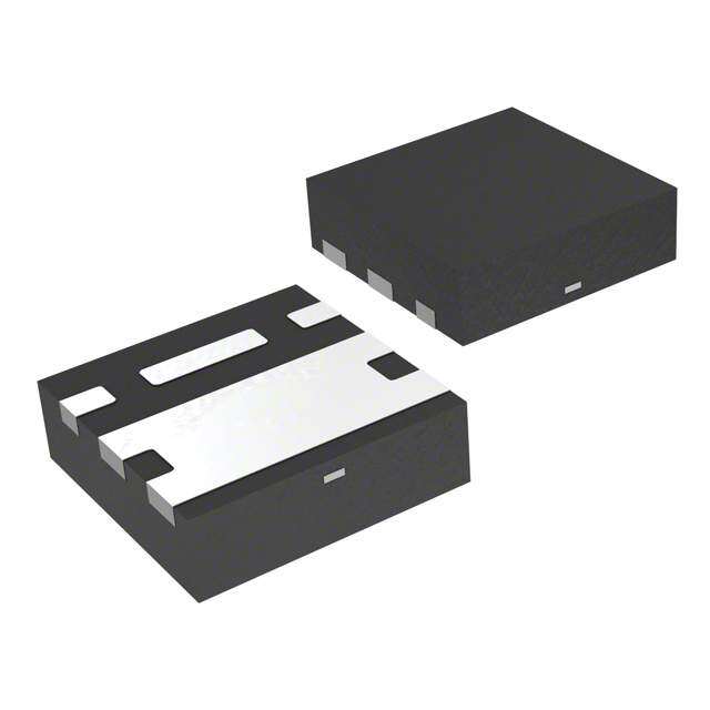
ICGOO电子元器件商城为您提供CSD25302Q2由Texas Instruments设计生产,在icgoo商城现货销售,并且可以通过原厂、代理商等渠道进行代购。 CSD25302Q2价格参考。Texas InstrumentsCSD25302Q2封装/规格:晶体管 - FET,MOSFET - 单, 表面贴装 P 沟道 20V 5A(Tc) 2.4W(Ta) 6-SON。您可以下载CSD25302Q2参考资料、Datasheet数据手册功能说明书,资料中有CSD25302Q2 详细功能的应用电路图电压和使用方法及教程。
Texas Instruments 的 CSD25302Q2 是一款 N 沟道增强型 MOSFET,属于小型功率 MOSFET,常用于需要高效能和小尺寸封装的应用场景。该器件采用 6 引脚 SC70 封装,具备低导通电阻(Rds(on))和快速开关特性,适合用于以下应用场景:

1. 电源管理:如 DC-DC 转换器、负载开关、电池管理系统等,因其低导通电阻可降低导通损耗,提高效率。

2. 电机驱动:适用于小型电机或步进电机的驱动电路,作为开关元件使用,具备良好的热稳定性和响应速度。

3. LED 驱动:在 LED 照明系统中用于调光控制或作为开关元件,支持高频 PWM 调光。

4. 工业控制:如 PLC 模块、传感器开关、继电器替代等,适用于需要高可靠性和小尺寸设计的工业环境。

5. 便携式设备:由于其小型封装和低功耗特性,适合用于智能手机、平板电脑、穿戴设备等便携电子产品中的电源开关或负载控制。

6. 汽车电子:如车载娱乐系统、LED 灯具控制、电池供电模块等,符合汽车级工作温度范围要求。

综上,CSD25302Q2 适用于需要高效、高速开关、空间受限的低至中功率应用场合。
| 参数 | 数值 |
| 产品目录 | |
| ChannelMode | Enhancement |
| 描述 | MOSFET PCH -20V -5A 6SONMOSFET PCh NexFET Pwr MOSFET |
| 产品分类 | FET - 单分离式半导体 |
| FET功能 | 逻辑电平门 |
| FET类型 | MOSFET P 通道,金属氧化物 |
| Id-ContinuousDrainCurrent | - 5 A |
| Id-连续漏极电流 | - 5 A |
| 品牌 | Texas Instruments |
| 产品手册 | |
| 产品图片 |
|
| rohs | 符合RoHS无铅 / 符合限制有害物质指令(RoHS)规范要求 |
| 产品系列 | 晶体管,MOSFET,Texas Instruments CSD25302Q2NexFET™ |
| 数据手册 | |
| 产品型号 | CSD25302Q2 |
| PCN过时产品 | |
| Pd-PowerDissipation | 2.4 W |
| Pd-功率耗散 | 2.4 W |
| Qg-GateCharge | 2.6 nC |
| Qg-栅极电荷 | 2.6 nC |
| RdsOn-Drain-SourceResistance | 49 mOhms |
| RdsOn-漏源导通电阻 | 49 mOhms |
| Vds-Drain-SourceBreakdownVoltage | - 20 V |
| Vds-漏源极击穿电压 | - 20 V |
| Vgs-Gate-SourceBreakdownVoltage | +/- 8 V |
| Vgs-栅源极击穿电压 | 8 V |
| 上升时间 | 13.2 ns |
| 下降时间 | 1.3 ns |
| 不同Id时的Vgs(th)(最大值) | 900mV @ 250µA |
| 不同Vds时的输入电容(Ciss) | 350pF @ 10V |
| 不同Vgs时的栅极电荷(Qg) | 3.4nC @ 4.5V |
| 不同 Id、Vgs时的 RdsOn(最大值) | 49 毫欧 @ 3A,4.5V |
| 产品培训模块 | http://www.digikey.cn/PTM/IndividualPTM.page?site=cn&lang=zhs&ptm=25585 |
| 产品目录页面 | |
| 产品种类 | MOSFET |
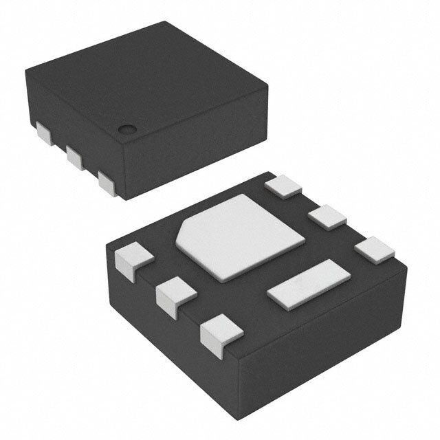
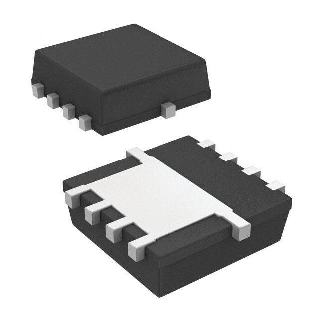
| 供应商器件封装 | 6-SON |
| 其它名称 | 296-25444-1 |
| 典型关闭延迟时间 | 8.6 ns |
| 制造商产品页 | http://www.ti.com/general/docs/suppproductinfo.tsp?distId=10&orderablePartNumber=CSD25302Q2 |
| 功率-最大值 | 2.4W |
| 包装 | 剪切带 (CT) |
| 商标 | Texas Instruments |
| 商标名 | NexFET |
| 安装类型 | 表面贴装 |
| 安装风格 | SMD/SMT |
| 封装 | Reel |
| 封装/外壳 | 6-SMD,扁平引线 |
| 封装/箱体 | WSON-6 FET |
| 工厂包装数量 | 3000 |
| 晶体管极性 | P-Channel |
| 最大工作温度 | + 150 C |
| 最小工作温度 | - 55 C |
| 标准包装 | 1 |
| 正向跨导-最小值 | 12.3 S |
| 漏源极电压(Vdss) | 20V |
| 电流-连续漏极(Id)(25°C时) | 5A (Tc) |
| 系列 | CSD25302Q2 |
| 视频文件 | http://www.digikey.cn/classic/video.aspx?PlayerID=1364138032001&width=640&height=455&videoID=541363338001http://www.digikey.cn/classic/video.aspx?PlayerID=1364138032001&width=640&height=455&videoID=1083957888001 |
| 通道模式 | Enhancement |
| 配置 | Single |


- 商务部:美国ITC正式对集成电路等产品启动337调查
- 曝三星4nm工艺存在良率问题 高通将骁龙8 Gen1或转产台积电
- 太阳诱电将投资9.5亿元在常州建新厂生产MLCC 预计2023年完工
- 英特尔发布欧洲新工厂建设计划 深化IDM 2.0 战略
- 台积电先进制程称霸业界 有大客户加持明年业绩稳了
- 达到5530亿美元!SIA预计今年全球半导体销售额将创下新高
- 英特尔拟将自动驾驶子公司Mobileye上市 估值或超500亿美元
- 三星加码芯片和SET,合并消费电子和移动部门,撤换高东真等 CEO
- 三星电子宣布重大人事变动 还合并消费电子和移动部门
- 海关总署:前11个月进口集成电路产品价值2.52万亿元 增长14.8%


PDF Datasheet 数据手册内容提取
CSD25302Q2 www.ti.com SLPS234B–NOVEMBER2009–REVISEDJANUARY2012 P-Channel NexFET™ Power MOSFET FEATURES 1 PRODUCTSUMMARY • UltralowQ andQ g gd VDS DraintoSourceVoltage –20 V • LowThermalResistance Qg GateChargeTotal(–4.5V) 2.6 nC • AvalancheRated Qgd GateChargeGatetoDrain 0.5 nC • PbFreeTerminalPlating VGS=–1.8V 71 mΩ • RoHSCompliant RDS(on) DraintoSourceOnResistance VGS=–2.5V 56 mΩ • HalogenFree VGS=–4.5V 39 mΩ • SON2-mm×2-mmPlasticPackage VGS(th) ThresholdVoltage –0.65 V ORDERINGINFORMATION APPLICATIONS Device Package Media Qty Ship • BatteryManagement SON2-mm×2-mm 13-Inch Tapeand CSD25302Q2 3000 • LoadManagement PlasticPackage Reel Reel • BatteryProtection ABSOLUTEMAXIMUMRATINGS DESCRIPTION TA=25°Cunlessotherwisestated VALUE UNIT The device has been designed to deliver the lowest VDS DraintoSourceVoltage –20 V on resistance and gate charge in the smallest outline VGS GatetoSourceVoltage ±8 V possible with excellent thermal characteristics in an ContinuousDrainCurrent,TC=25°C –5 A ultra low profile. Low on resistance coupled with the ID ContinuousDrainCurrent(1) –5 A extremely small footprint and low profile make the IDM PulsedDrainCurrent,TA=25°C(2) –20 A device ideal for battery operated space constrained PD PowerDissipation 2.4 W applications. TJ, OperatingJunctionandStorage –55to150 °C TSTG TemperatureRange TopView (1) PackageLimited (2) Pulseduration10µs,dutycycle≤2% S 1 6 S S S 2 5 S G 3 D 4 D P0112-01 R vsV GATECHARGE DS(on) GS 150 6 Wm ID = −3A ID=−3A ce − 125 −V 5 VDS=−10V − On-State Resistan 1570050 TC = 125°C V−Gate VoltageGS 234 R DS(on) 25 TC = 25°C − 1 0 0 1 2 3 4 5 6 7 8 0.0 0.5 1.0 1.5 2.0 2.5 3.0 −VGS − Gate to Source Voltage − V G006 Qg−Gate Charge−nC G003 1 Pleasebeawarethatanimportantnoticeconcerningavailability,standardwarranty,anduseincriticalapplicationsofTexas Instrumentssemiconductorproductsanddisclaimerstheretoappearsattheendofthisdatasheet. PRODUCTIONDATAinformationiscurrentasofpublicationdate. Copyright©2009–2012,TexasInstrumentsIncorporated Products conform to specifications per the terms of the Texas Instruments standard warranty. Production processing does not necessarilyincludetestingofallparameters.
CSD25302Q2 SLPS234B–NOVEMBER2009–REVISEDJANUARY2012 www.ti.com Thesedeviceshavelimitedbuilt-inESDprotection.Theleadsshouldbeshortedtogetherorthedeviceplacedinconductivefoam duringstorageorhandlingtopreventelectrostaticdamagetotheMOSgates. ELECTRICAL CHARACTERISTICS T =25°C,unlessotherwisespecified A PARAMETER TESTCONDITIONS MIN TYP MAX UNIT StaticCharacteristics BV DraintoSourceVoltage V =0V,I =–250μA –20 V DSS GS DS I DraintoSourceLeakage V =0V,V =–16V –1 μA DSS GS DS I GatetoSourceLeakage V =0V,V =±8V –100 nA GSS DS GS V GatetoSourceThresholdVoltage V =V ,I =–250μA –0.5 –0.65 –0.9 V GS(th) DS GS DS V =–1.8V,I =–3.0A 71 92 mΩ GS DS R DraintoSourceOnResistance V =–2.5V,I =–3.0A 56 70 mΩ DS(on) GS DS V =–4.5V,I =–3.0A 39 49 mΩ GS DS g Transconductance V =–10V,I =–3.0A 12.3 S fs DS DS DynamicCharacteristics C InputCapacitance 270 350 pF ISS C OutputCapacitance V =0V,V =–10V,f=1MHz 120 150 pF OSS GS DS C ReverseTransferCapacitance 40 55 pF RSS Q GateChargeTotal(–4.5V) 2.6 3.4 nC g Q GateCharge–GatetoDrain 0.5 nC gd V =–10V,I =–3.0A DS DS Q GateChargeGatetoSource 0.54 nC gs Qg(th) GateChargeatVth 0.2 nC Q OutputCharge V =–13V,V =0V 2.3 nC OSS DS GS t TurnOnDelayTime 3.2 ns d(on) t RiseTime 13.2 ns r V =–10V,V =–4.5V,I =–3.0A,R =2Ω DS GS DS G t TurnOffDelayTime 8.6 ns d(off) t FallTime 1.3 ns f DiodeCharacteristics V DiodeForwardVoltage I =–3.0A,V =0V –0.8 –1.0 V SD DS GS Q ReverseRecoveryCharge 2.5 nC rr V =–13V,I =–3.0A,di/dt=300A/μs dd F t ReverseRecoveryTime 8.8 ns rr THERMAL CHARACTERISTICS T =25°C,unlessotherwisespecified A PARAMETER MIN TYP MAX UNIT R ThermalResistanceJunctiontoCase(1) 8.6 °C/W θJC R ThermalResistanceJunctiontoAmbient(1)(2) 66 °C/W θJA (1) R isdeterminedwiththedevicemountedona1-inch2(6.45-cm2),2-oz.(0.071-mmthick)Cupadona1.5-inch×1.5-inch(3.81-cm× θJC 3.81-cm),0.06-inch(1.52-mm)thickFR4PCB.R isspecifiedbydesign,whereasR isdeterminedbytheuser’sboarddesign. θJC θJA (2) DevicemountedonFR4materialwith1-inch2(6.45-cm2),2-oz.(0.071-mmthick)Cu. 2 SubmitDocumentationFeedback Copyright©2009–2012,TexasInstrumentsIncorporated
CSD25302Q2 www.ti.com SLPS234B–NOVEMBER2009–REVISEDJANUARY2012 GATE Source GATE Source MaxR =66°C/W MaxR =207°C/W θJA θJA whenmountedon whenmountedon 1inch2(6.45cm2)of minimumpadareaof 2-oz.(0.071-mmthick) 2-oz.(0.071-mmthick) Cu. Cu. DRAIN DRAIN M0161-01 M0161-02 TYPICAL MOSFET CHARACTERISTICS T =25°C,unlessotherwisespecified A 10 e c n a d 1 e p m 0.5 al I 0.3 m er Th 0.1 0.1 Duty Cycle = t1/t2 d e 0.05 z ali P m 0.02 Nor 0.01 t1 Z − qJA 0.01 Single Pulse Typical Rq JA =t2 166°C/W (min Cu) TJ = P × Zq JA × Rq JA 0.001 0.0001 0.001 0.01 0.1 1 10 100 1k tP − Pulse Duration − s G012 Figure1. TransientThermalImpedance Copyright©2009–2012,TexasInstrumentsIncorporated SubmitDocumentationFeedback 3
CSD25302Q2 SLPS234B–NOVEMBER2009–REVISEDJANUARY2012 www.ti.com TYPICAL MOSFET CHARACTERISTICS (continued) T =25°C,unlessotherwisespecified A 5.0 5.0 4.5 4.5 VDS = −5V 4.0 4.0 A A − 3.5 − 3.5 Current 23..50 VVGGSS = = − −34.5.5VV Current 23..50 TC = 125°C Drain 2.0 VGS = −2.5V Drain 2.0 TC = 25°C − D 1.5 VGS = −2V − D 1.5 −I 1.0 VGS = −1.8V −I 1.0 0.5 0.5 TC = −55°C 0.0 0.0 0.0 0.2 0.4 0.6 0.8 1.0 0.5 0.7 0.9 1.1 1.3 1.5 −VDS − Drain to Source Voltage − V G001 −VGS − Gate to Source Voltage − V G002 Figure2.SaturationCharacteristics Figure3.TransferCharacteristics 6 0.4 ID=−3A f = 1MHz V 5 VDS=−10V VGS = 0V − F 0.3 e n Voltag 4 nce − COSS = CDS + CGD Gate 3 pacita 0.2 CISS = CGD + CGS − a VGS 2 C − C 0.1 CRSS = CGD − 1 0 0.0 0.0 0.5 1.0 1.5 2.0 2.5 3.0 0 5 10 15 20 Qg−Gate Charge−nC G003 −VDS − Drain to Source Voltage − V G004 Figure4.GateCharge Figure5.Capacitance 0.9 150 V 0.8 ID = −250m A Wm ID = −3A − − 125 e 0.7 e g c a n hreshold Volt 000...456 State Resista 17050 TC = 125°C −V − TGS(th) 000...123 R − On-DS(on) 2550 TC = 25°C 0.0 0 −75 −25 25 75 125 175 1 2 3 4 5 6 7 8 TC − Case Temperature − °C G005 −VGS − Gate to Source Voltage − V G006 Figure6.ThresholdVoltagevs.Temperature Figure7.On-StateResistancevs.GatetoSourceVoltage 4 SubmitDocumentationFeedback Copyright©2009–2012,TexasInstrumentsIncorporated
CSD25302Q2 www.ti.com SLPS234B–NOVEMBER2009–REVISEDJANUARY2012 TYPICAL MOSFET CHARACTERISTICS (continued) T =25°C,unlessotherwisespecified A 1.6 10 ance 1.4 IVDG =S −=3 −A4.5V nt − A 1 State Resist 011...802 Drain Curre 0.1 TC = 125°C malized On- 00..46 − Source to 00.0.0011 TC = 25°C Nor 0.2 −I SD 0.0 0.0001 −75 −25 25 75 125 175 0.0 0.2 0.4 0.6 0.8 1.0 TC − Case Temperature − °C G007 −VSD − Source to Drain Voltage − V G008 Figure8.NormalizedOn-StateResistancevs.Temperature Figure9.TypicalDiodeForwardVoltage 100 6 5 A 10 A − − nt nt 4 e e urr 1ms urr n C 1 10ms n C 3 ai ai − Dr Area Limited 100ms − Dr 2 −I D 0.1 by RDS(on) 1s −I D 1 Single Pulse DC Typical Rq JA = 166°C/W (min Cu) 0.01 0 0.01 0.1 1 10 100 −50 −25 0 25 50 75 100 125 150 175 −VD − Drain Voltage − V G009 TC − Case Temperature − °C G011 Figure10.MaximumSafeOperatingArea Figure11. MaximumDrainCurrentvs.Temperature Copyright©2009–2012,TexasInstrumentsIncorporated SubmitDocumentationFeedback 5
CSD25302Q2 SLPS234B–NOVEMBER2009–REVISEDJANUARY2012 www.ti.com MECHANICAL DATA Q2 Package Dimensions D2 D K2 K1 K3 K 6 5 4 4 5 6 2 3 E E 7 E 8 1 E 4 K 1 2 3 3 2 1 Pin 1 Dot b e Pin 1 ID Top View L D1 Bottom View C Pinout A1 A Source 1, 2, 5, 6, 8 Gate 3 Drain 4, 7 Front View M0175-01 MILLIMETERS INCHES DIM MIN NOM MAX MIN NOM MAX A 0.700 0.750 0.800 0.028 0.030 0.032 A1 0.000 0.050 0.000 0.002 b 0.250 0.300 0.350 0.010 0.012 0.014 C 0.203TYP 0.008TYP D 2.000TYP 0.080TYP D1 0.900 0.950 1.000 0.036 0.038 0.040 D2 0.300TYP 0.012TYP E 2.000TYP 0.080TYP E1 0.900 1.000 1.100 0.036 0.040 0.044 E2 0.280TYP 0.0112TYP E3 0.470TYP 0.0188TYP e 0.650BSC 0.026TYP K 0.280TYP 0.0112TYP K1 0.350TYP 0.014TYP K2 0.200TYP 0.008TYP K3 0.200TYP 0.008TYP K4 0.470TYP 0.0188TYP L 0.200 0.25 0.300 0.008 0.010 0.0121 6 SubmitDocumentationFeedback Copyright©2009–2012,TexasInstrumentsIncorporated
CSD25302Q2 www.ti.com SLPS234B–NOVEMBER2009–REVISEDJANUARY2012 Recommended PCB Pattern 0.65TYP 5 2.30 1.10 1.05 0.8 0.22 1.40 1 0.46 0.40TYP 0.25 M0167-01 Note: Alldimensionsareinmm,unlessotherwisespecified. For recommended circuit layout for PCB designs, see application note SLPA005 – Reducing Ringing throughPCBLayoutTechniques. Q2 Tape and Reel Information 4.00 ±0.10 2.00 ±0.05 Ø 1.50 ±0.10 0.300.10 0.10 10° Max +– ± 0 5 0 7 8. 1. 5 0 0. ± 5 50 0.0 3. 0 ± 4.00 ±0.10 Ø 1.00 ±0.25 3 2. 1.00 ±0.05 0.254 ±0.02 10° Max 2.30 ±0.05 M0168-01 Notes: 1.Measuredfromcenterlineofsprocketholetocenterlineofpocket 2.Cumulativetoleranceof10sprocketholesis±0.20 3.Othermaterialavailable 4.TypicalSRofformtapeMax108OHM/SQ 5.Alldimensionsareinmm,unlessotherwisespecified. Copyright©2009–2012,TexasInstrumentsIncorporated SubmitDocumentationFeedback 7
CSD25302Q2 SLPS234B–NOVEMBER2009–REVISEDJANUARY2012 www.ti.com REVISION HISTORY ChangesfromOriginal(November2009)toRevisionA Page • DeletedthePackageMarkingInformationsection ............................................................................................................... 8 ChangesfromRevisionA(October2010)toRevisionB Page • AddedESDSstatement ........................................................................................................................................................ 2 8 SubmitDocumentationFeedback Copyright©2009–2012,TexasInstrumentsIncorporated
IMPORTANTNOTICE TexasInstrumentsIncorporatedanditssubsidiaries(TI)reservetherighttomakecorrections,modifications,enhancements,improvements, andotherchangestoitsproductsandservicesatanytimeandtodiscontinueanyproductorservicewithoutnotice.Customersshould obtainthelatestrelevantinformationbeforeplacingordersandshouldverifythatsuchinformationiscurrentandcomplete.Allproductsare soldsubjecttoTI’stermsandconditionsofsalesuppliedatthetimeoforderacknowledgment. TIwarrantsperformanceofitshardwareproductstothespecificationsapplicableatthetimeofsaleinaccordancewithTI’sstandard warranty.TestingandotherqualitycontroltechniquesareusedtotheextentTIdeemsnecessarytosupportthiswarranty.Exceptwhere mandatedbygovernmentrequirements,testingofallparametersofeachproductisnotnecessarilyperformed. TIassumesnoliabilityforapplicationsassistanceorcustomerproductdesign.Customersareresponsiblefortheirproductsand applicationsusingTIcomponents.Tominimizetherisksassociatedwithcustomerproductsandapplications,customersshouldprovide adequatedesignandoperatingsafeguards. TIdoesnotwarrantorrepresentthatanylicense,eitherexpressorimplied,isgrantedunderanyTIpatentright,copyright,maskworkright, orotherTIintellectualpropertyrightrelatingtoanycombination,machine,orprocessinwhichTIproductsorservicesareused.Information publishedbyTIregardingthird-partyproductsorservicesdoesnotconstitutealicensefromTItousesuchproductsorservicesora warrantyorendorsementthereof.Useofsuchinformationmayrequirealicensefromathirdpartyunderthepatentsorotherintellectual propertyofthethirdparty,oralicensefromTIunderthepatentsorotherintellectualpropertyofTI. ReproductionofTIinformationinTIdatabooksordatasheetsispermissibleonlyifreproductioniswithoutalterationandisaccompanied byallassociatedwarranties,conditions,limitations,andnotices.Reproductionofthisinformationwithalterationisanunfairanddeceptive businesspractice.TIisnotresponsibleorliableforsuchaltereddocumentation.Informationofthirdpartiesmaybesubjecttoadditional restrictions. ResaleofTIproductsorserviceswithstatementsdifferentfromorbeyondtheparametersstatedbyTIforthatproductorservicevoidsall expressandanyimpliedwarrantiesfortheassociatedTIproductorserviceandisanunfairanddeceptivebusinesspractice.TIisnot responsibleorliableforanysuchstatements. TIproductsarenotauthorizedforuseinsafety-criticalapplications(suchaslifesupport)whereafailureoftheTIproductwouldreasonably beexpectedtocauseseverepersonalinjuryordeath,unlessofficersofthepartieshaveexecutedanagreementspecificallygoverning suchuse.Buyersrepresentthattheyhaveallnecessaryexpertiseinthesafetyandregulatoryramificationsoftheirapplications,and acknowledgeandagreethattheyaresolelyresponsibleforalllegal,regulatoryandsafety-relatedrequirementsconcerningtheirproducts andanyuseofTIproductsinsuchsafety-criticalapplications,notwithstandinganyapplications-relatedinformationorsupportthatmaybe providedbyTI.Further,BuyersmustfullyindemnifyTIanditsrepresentativesagainstanydamagesarisingoutoftheuseofTIproductsin suchsafety-criticalapplications. TIproductsareneitherdesignednorintendedforuseinmilitary/aerospaceapplicationsorenvironmentsunlesstheTIproductsare specificallydesignatedbyTIasmilitary-gradeor"enhancedplastic."OnlyproductsdesignatedbyTIasmilitary-grademeetmilitary specifications.BuyersacknowledgeandagreethatanysuchuseofTIproductswhichTIhasnotdesignatedasmilitary-gradeissolelyat theBuyer'srisk,andthattheyaresolelyresponsibleforcompliancewithalllegalandregulatoryrequirementsinconnectionwithsuchuse. TIproductsareneitherdesignednorintendedforuseinautomotiveapplicationsorenvironmentsunlessthespecificTIproductsare designatedbyTIascompliantwithISO/TS16949requirements.Buyersacknowledgeandagreethat,iftheyuseanynon-designated productsinautomotiveapplications,TIwillnotberesponsibleforanyfailuretomeetsuchrequirements. FollowingareURLswhereyoucanobtaininformationonotherTexasInstrumentsproductsandapplicationsolutions: Products Applications Audio www.ti.com/audio AutomotiveandTransportation www.ti.com/automotive Amplifiers amplifier.ti.com CommunicationsandTelecom www.ti.com/communications DataConverters dataconverter.ti.com ComputersandPeripherals www.ti.com/computers DLP®Products www.dlp.com ConsumerElectronics www.ti.com/consumer-apps DSP dsp.ti.com EnergyandLighting www.ti.com/energy ClocksandTimers www.ti.com/clocks Industrial www.ti.com/industrial Interface interface.ti.com Medical www.ti.com/medical Logic logic.ti.com Security www.ti.com/security PowerMgmt power.ti.com Space,AvionicsandDefense www.ti.com/space-avionics-defense Microcontrollers microcontroller.ti.com VideoandImaging www.ti.com/video RFID www.ti-rfid.com OMAPMobileProcessors www.ti.com/omap WirelessConnectivity www.ti.com/wirelessconnectivity TIE2ECommunityHomePage e2e.ti.com MailingAddress:TexasInstruments,PostOfficeBox655303,Dallas,Texas75265 Copyright©2012,TexasInstrumentsIncorporated