ICGOO在线商城 > 分立半导体产品 > 晶体管 - FET,MOSFET - 单 > IRFP22N50APBF
 Datasheet下载
- 型号: IRFP22N50APBF
- 制造商: Vishay
- 库位|库存: xxxx|xxxx
- 要求:
| 数量阶梯 | 香港交货 | 国内含税 |
| +xxxx | $xxxx | ¥xxxx |
查看当月历史价格
查看今年历史价格
IRFP22N50APBF产品简介:
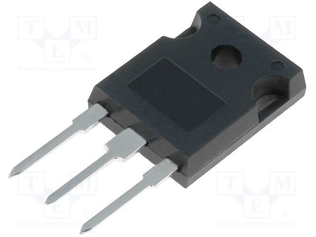
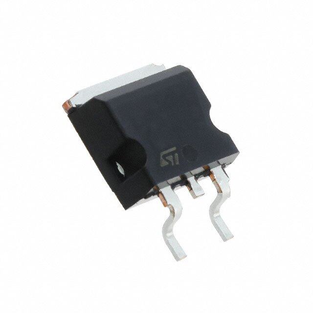
ICGOO电子元器件商城为您提供IRFP22N50APBF由Vishay设计生产,在icgoo商城现货销售,并且可以通过原厂、代理商等渠道进行代购。 IRFP22N50APBF价格参考¥12.87-¥16.08。VishayIRFP22N50APBF封装/规格:晶体管 - FET,MOSFET - 单, 通孔 N 沟道 500V 22A(Tc) 277W(Tc) TO-247-3。您可以下载IRFP22N50APBF参考资料、Datasheet数据手册功能说明书,资料中有IRFP22N50APBF 详细功能的应用电路图电压和使用方法及教程。
Vishay Siliconix的IRFP22N50APBF是一款N沟道增强型MOSFET(金属氧化物场效应晶体管),其应用场景广泛,尤其适用于高电压和中等电流的应用场合。以下是该型号MOSFET的一些典型应用场景:

1. 电源管理:
   - IRFP22N50APBF常用于开关电源(SMPS)中,作为主开关器件。其高击穿电压(500V)使其能够承受较高的输入电压,适用于工业电源、通信设备电源以及不间断电源(UPS)系统。

2. 电机驱动:
   - 在电动工具、家用电器和工业自动化设备中,该MOSFET可用于驱动直流电机或步进电机。它能够快速切换状态,提供高效的功率传输,并且具有较低的导通电阻(Rds(on)),从而减少能量损耗。

3. 逆变器和转换器:
   - 该MOSFET适用于太阳能逆变器、DC-DC转换器等电力电子设备。它可以高效地进行电能转换,确保系统的稳定性和效率。

4. 电磁兼容性(EMC)设计:
   - 在需要考虑电磁干扰(EMI)的设计中,IRFP22N50APBF的快速开关特性和低噪声性能有助于减少电磁辐射,满足严格的EMC标准。

5. 保护电路:
   - 该MOSFET可以用作过流保护、短路保护等安全功能的关键元件。其内置的雪崩击穿能力使其能够在异常情况下吸收瞬态能量,保护整个电路免受损坏。

6. 脉宽调制(PWM)控制:
   - 在LED照明、音频放大器等领域,IRFP22N50APBF可以用于PWM调光或调速控制。它能够精确调节输出功率,实现节能和性能优化。

总之,IRFP22N50APBF凭借其出色的电气特性,在多种电力电子应用中表现出色,特别是在需要高可靠性和高效能的场景下。
| 参数 | 数值 |
| 产品目录 | |
| ChannelMode | Enhancement |
| 描述 | MOSFET N-CH 500V 22A TO-247ACMOSFET N-Chan 500V 22 Amp |
| 产品分类 | FET - 单分离式半导体 |
| FET功能 | 标准 |
| FET类型 | MOSFET N 通道,金属氧化物 |
| Id-ContinuousDrainCurrent | 22 A |
| Id-连续漏极电流 | 22 A |
| 品牌 | Vishay SiliconixVishay / Siliconix |
| 产品手册 | |
| 产品图片 |
|
| rohs | RoHS 合规性豁免无铅 / 符合限制有害物质指令(RoHS)规范要求 |
| 产品系列 | 晶体管,MOSFET,Vishay / Siliconix IRFP22N50APBF- |
| 数据手册 | |
| 产品型号 | IRFP22N50APBFIRFP22N50APBF |
| Pd-PowerDissipation | 277 W |
| Pd-功率耗散 | 277 W |
| RdsOn-Drain-SourceResistance | 230 mOhms |
| RdsOn-漏源导通电阻 | 230 mOhms |
| Vds-Drain-SourceBreakdownVoltage | 500 V |
| Vds-漏源极击穿电压 | 500 V |
| Vgs-Gate-SourceBreakdownVoltage | +/- 30 V |
| Vgs-栅源极击穿电压 | 30 V |
| 上升时间 | 94 ns |
| 下降时间 | 47 ns |
| 不同Id时的Vgs(th)(最大值) | 4V @ 250µA |
| 不同Vds时的输入电容(Ciss) | 3450pF @ 25V |
| 不同Vgs时的栅极电荷(Qg) | 120nC @ 10V |
| 不同 Id、Vgs时的 RdsOn(最大值) | 230 毫欧 @ 13A,10V |
| 产品目录绘图 |
|
| 产品目录页面 | |
| 产品种类 | MOSFET |
| 供应商器件封装 | TO-247-3 |
| 其它名称 | *IRFP22N50APBF |
| 典型关闭延迟时间 | 47 ns |
| 功率-最大值 | 277W |
| 功率耗散 | 277 W |
| 包装 | 管件 |
| 商标 | Vishay / Siliconix |
| 安装类型 | 通孔 |
| 安装风格 | Through Hole |
| 导通电阻 | 230 mOhms |
| 封装 | Tube |
| 封装/外壳 | TO-247-3 |
| 封装/箱体 | TO-247-3 |
| 工厂包装数量 | 500 |
| 晶体管极性 | N-Channel |
| 最大工作温度 | + 150 C |
| 最小工作温度 | - 55 C |
| 标准包装 | 25 |
| 汲极/源极击穿电压 | 500 V |
| 漏极连续电流 | 22 A |
| 漏源极电压(Vdss) | 500V |
| 电流-连续漏极(Id)(25°C时) | 22A (Tc) |
| 通道模式 | Enhancement |
| 配置 | Single |
| 闸/源击穿电压 | +/- 30 V |


- 商务部:美国ITC正式对集成电路等产品启动337调查
- 曝三星4nm工艺存在良率问题 高通将骁龙8 Gen1或转产台积电
- 太阳诱电将投资9.5亿元在常州建新厂生产MLCC 预计2023年完工
- 英特尔发布欧洲新工厂建设计划 深化IDM 2.0 战略
- 台积电先进制程称霸业界 有大客户加持明年业绩稳了
- 达到5530亿美元!SIA预计今年全球半导体销售额将创下新高
- 英特尔拟将自动驾驶子公司Mobileye上市 估值或超500亿美元
- 三星加码芯片和SET,合并消费电子和移动部门,撤换高东真等 CEO
- 三星电子宣布重大人事变动 还合并消费电子和移动部门
- 海关总署:前11个月进口集成电路产品价值2.52万亿元 增长14.8%


PDF Datasheet 数据手册内容提取
IRFP22N50A, SiHFP22N50A Vishay Siliconix Power MOSFET FEATURES PRODUCT SUMMARY • Low Gate Charge Q Results in Simple Drive V (V) 500 g DS Requirement Available RDS(on) () VGS = 10 V 0.23 RoHS* (cid:129) Improved Gate, Avalanche and Dynamic dV/dt Qg (Max.) (nC) 120 Ruggedness COMPLIANT Q (nC) 32 gs (cid:129) Fully Characterized Capacitance and Avalanche Voltage Q (nC) 52 gd and Current Configuration Single (cid:129) Compliant to RoHS Directive 2002/95/EC D TO-247AC APPLICATIONS (cid:129) Switch Mode Power Supply (SMPS) (cid:129) Uninterruptable Power Supply G (cid:129) High Speed Power Switching S D TYPICAL SMPS TOPOLOGIES G S (cid:129) Full Bridge Converters N-Channel MOSFET (cid:129) Power Factor Correction Boost ORDERING INFORMATION Package TO-247AC IRFP22N50APbF Lead (Pb)-free SiHFP22N50A-E3 IRFP22N50A SnPb SiHFP22N50A ABSOLUTE MAXIMUM RATINGS (T = 25 °C, unless otherwise noted) C PARAMETER SYMBOL LIMIT UNIT Drain-Source Voltage V 500 DS V Gate-Source Voltage V ± 30 GS T = 25 °C 22 Continuous Drain Current V at 10 V C I GS D T = 100 °C 14 A C Pulsed Drain Currenta I 88 DM Linear Derating Factor 2.2 W/°C Single Pulse Avalanche Energyb E 1180 mJ AS Repetitive Avalanche Currenta I 22 A AR Repetitive Avalanche Energya E 28 mJ AR Maximum Power Dissipation T = 25 °C P 277 W C D Peak Diode Recovery dV/dtc dV/dt 4.8 V/ns Operating Junction and Storage Temperature Range T, T - 55 to + 150 J stg °C Soldering Recommendations (Peak Temperature) for 10 s 300d 10 lbf · in Mounting Torque 6-32 or M3 screw 1.1 N · m Notes a. Repetitive rating; pulse width limited by maximum junction temperature (see fig. 11). b. Starting TJ = 25 °C, L = 4.87 mH, Rg = 25 , IAS = 22 A (see fig. 12). c. ISD 22 A, dI/dt 190 A/µs, VDD VDS, TJ 150 °C. d. 1.6 mm from case. * Pb containing terminations are not RoHS compliant, exemptions may apply Document Number: 91207 www.vishay.com S11-0446-Rev. C, 14-Mar-11 1 This datasheet is subject to change without notice. THE PRODUCT DESCRIBED HEREIN AND THIS DATASHEET ARE SUBJECT TO SPECIFIC DISCLAIMERS, SET FORTH AT
IRFP22N50A, SiHFP22N50A Vishay Siliconix THERMAL RESISTANCE RATINGS PARAMETER SYMBOL TYP. MAX. UNIT Maximum Junction-to-Ambient R - 40 thJA Case-to-Sink, Flat, Greased Surface R 0.24 - °C/W thCS Maximum Junction-to-Case (Drain) R - 0.45 thJC SPECIFICATIONS (T = 25 °C, unless otherwise noted) J PARAMETER SYMBOL TEST CONDITIONS MIN. TYP. MAX. UNIT Static Drain-Source Breakdown Voltage VDS VGS = 0 V, ID = 250 µA 500 - - V VDS Temperature Coefficient VDS/TJ Reference to 25 °C, ID = 1 mA - 0.55 - V/°C Gate-Source Threshold Voltage VGS(th) VDS = VGS, ID = 250 µA 2.0 - 4.0 V Gate-Source Leakage I V = ± 30 V - - ± 100 nA GSS GS V = 500 V, V = 0 V - - 25 DS GS Zero Gate Voltage Drain Current I µA DSS V = 400 V, V = 0 V, T = 125 °C - - 250 DS GS J Drain-Source On-State Resistance RDS(on) VGS = 10 V ID = 13 Ab - - 0.23 Forward Transconductance g V = 50 V, I = 13 Ab 12 - - S fs DS D Dynamic Input Capacitance C - 3450 - iss V = 0 V, GS Output Capacitance C V = 25 V, - 513 - oss DS f = 1.0 MHz, see fig. 5 Reverse Transfer Capacitance C - 27 - rss pF V = 1.0 V, f = 1.0 MHz 4935 DS Output Capacitance C oss V = 0 V V = 400 V, f = 1.0 MHz 137 GS DS Effective Output Capacitance C eff. V = 0 V to 400 Vc 264 oss DS Total Gate Charge Q - - 120 g I = 22 A, V = 400 V, Gate-Source Charge Q V = 10 V D DS - - 32 nC gs GS see fig. 6 and 13b Gate-Drain Charge Q - - 52 gd Turn-On Delay Time t - 26 - d(on) Rise Time t - 94 - r VDD = 250 V, ID = 22 A, ns Turn-Off Delay Time td(off) RG = 4.3 , RD = 11, see fig. 10b - 47 - Fall Time t - 47 - f Drain-Source Body Diode Characteristics MOSFET symbol Continuous Source-Drain Diode Current IS showing the D - - 22 integral reverse A G Pulsed Diode Forward Currenta I p - n junction diode - - 88 SM S Body Diode Voltage V T = 25 °C, I = 22A, V = 0 Vb - - 1.5 V SD J S GS Body Diode Reverse Recovery Time t - 570 850 ns rr T = 25 °C, I = 22 A, dI/dt = 100 A/µsb J F Body Diode Reverse Recovery Charge Q - 6.1 9.2 µC rr Forward Turn-On Time t Intrinsic turn-on time is negligible (turn-on is dominated by L and L ) on S D Notes a. Repetitive rating; pulse width limited by maximum junction temperature (see fig. 11). b. Pulse width 300 µs; duty cycle 2 %. c. C eff. is a fixed capacitance that gives the same charging time as C while V is rising from 0 % to 80 % V . oss oss DS DS www.vishay.com Document Number: 91207 2 S11-0446-Rev. C, 14-Mar-11 This datasheet is subject to change without notice. THE PRODUCT DESCRIBED HEREIN AND THIS DATASHEET ARE SUBJECT TO SPECIFIC DISCLAIMERS, SET FORTH AT
IRFP22N50A, SiHFP22N50A Vishay Siliconix TYPICAL CHARACTERISTICS (25 °C, unless otherwise noted) Fig. 1 - Typical Output Characteristics Fig. 3 - Typical Transfer Characteristics Fig. 2 - Typical Output Characteristics Fig. 4 - Normalized On-Resistance vs. Temperature Document Number: 91207 www.vishay.com S11-0446-Rev. C, 14-Mar-11 3 This datasheet is subject to change without notice. THE PRODUCT DESCRIBED HEREIN AND THIS DATASHEET ARE SUBJECT TO SPECIFIC DISCLAIMERS, SET FORTH AT
IRFP22N50A, SiHFP22N50A Vishay Siliconix Fig. 5 - Typical Capacitance vs. Drain-to-Source Voltage Fig. 7 - Typical Source-Drain Diode Forward Voltage Fig. 6 - Typical Gate Charge vs. Gate-to-Source Voltage Fig. 8 - Maximum Safe Operating Area www.vishay.com Document Number: 91207 4 S11-0446-Rev. C, 14-Mar-11 This datasheet is subject to change without notice. THE PRODUCT DESCRIBED HEREIN AND THIS DATASHEET ARE SUBJECT TO SPECIFIC DISCLAIMERS, SET FORTH AT
IRFP22N50A, SiHFP22N50A Vishay Siliconix R D V DS V GS D.U.T. R G + -VDD 10 V Pulse width ≤ 1 µs Duty factor ≤ 0.1 % Fig. 10a - Switching Time Test Circuit V DS 90 % 10 % V GS t t t t d(on) r d(off) f Fig. 9 - Maximum Drain Current vs. Case Temperature Fig. 10b - Switching Time Waveforms Fig. 11 - Maximum Effective Transient Thermal Impedance, Junction-to-Case L VDS V Vary tp to obtain DS tp required I V AS DD RG D.U.T + V I - DD A VDS AS 10 V tp 0.01 Ω I AS Fig. 12a - Unclamped Inductive Test Circuit Fig. 12b - Unclamped Inductive Waveforms Document Number: 91207 www.vishay.com S11-0446-Rev. C, 14-Mar-11 5 This datasheet is subject to change without notice. THE PRODUCT DESCRIBED HEREIN AND THIS DATASHEET ARE SUBJECT TO SPECIFIC DISCLAIMERS, SET FORTH AT
IRFP22N50A, SiHFP22N50A Vishay Siliconix Fig. 12c - Maximum Avalanche Energy vs. Drain Current Fig. 12d - Typical Drain-to-Source Voltage vs. Avalanche Current Current regulator Same type as D.U.T. Q 50 kΩ G 10 V 12 V 0.2 µF 0.3 µF QGS QGD + V D.U.T. - DS V G V GS 3 mA Charge I I G D Current sampling resistors Fig. 13b - Gate Charge Test Circuit Fig. 13a - Basic Gate Charge Waveform www.vishay.com Document Number: 91207 6 S11-0446-Rev. C, 14-Mar-11 This datasheet is subject to change without notice. THE PRODUCT DESCRIBED HEREIN AND THIS DATASHEET ARE SUBJECT TO SPECIFIC DISCLAIMERS, SET FORTH AT
IRFP22N50A, SiHFP22N50A Vishay Siliconix Peak Diode Recovery dV/dt Test Circuit + Circuit layout considerations D.U.T. (cid:129) Low stray inductance (cid:129) Ground plane (cid:129) Low leakage inductance current transformer - + - + - Rg (cid:129) dV/dt controlled by Rg + (cid:129) Driver same type as D.U.T. V - DD (cid:129) ISD controlled by duty factor “D” (cid:129) D.U.T. - device under test Driver gate drive Period D = P.W. P.W. Period V = 10 Va GS D.U.T. l waveform SD Reverse recovery Body diode forward current current dI/dt D.U.T. V waveform DS Diode recovery dV/dt V DD Re-applied voltage Body diode forward drop Inductor current Ripple ≤ 5 % ISD Note a. V = 5 V for logic level devices GS Fig. 14 - For N-Channel Vishay Siliconix maintains worldwide manufacturing capability. Products may be manufactured at one of several qualified locations. Reliability data for Silicon Technology and Package Reliability represent a composite of all qualified locations. For related documents such as package/tape drawings, part marking, and reliability data, see www.vishay.com/ppg?91207. Document Number: 91207 www.vishay.com S11-0446-Rev. C, 14-Mar-11 7 This datasheet is subject to change without notice. THE PRODUCT DESCRIBED HEREIN AND THIS DATASHEET ARE SUBJECT TO SPECIFIC DISCLAIMERS, SET FORTH AT
Package Information www.vishay.com Vishay Siliconix TO-247AC (High Voltage) 4 A A B E 7 ØP (Datum B) E/2 S A2 Ø kMDBM 3 R/2 ØP1 A D2 Q 2 x R 4 4 (2) D D1 1 2 3 D 4 Thermal pad 5 L1 C L 4 E1 See view B A 0.01MDBM 2 x b2 C View A - A 2 x e 3 x b b4 A1 0.10MCAM (b1, b3, b5) Planting Base metal Lead Assignments 1. Gate D DE E 2. Drain 3. Source C C (c) c1 4. Drain (b, b2, b4) (4) Section C - C, D - D, E - E View B MILLIMETERS INCHES MILLIMETERS INCHES DIM. MIN. MAX. MIN. MAX. DIM. MIN. MAX. MIN. MAX. A 4.58 5.31 0.180 0.209 D2 0.51 1.30 0.020 0.051 A1 2.21 2.59 0.087 0.102 E 15.29 15.87 0.602 0.625 A2 1.17 2.49 0.046 0.098 E1 13.72 - 0.540 - b 0.99 1.40 0.039 0.055 e 5.46 BSC 0.215 BSC b1 0.99 1.35 0.039 0.053 Ø k 0.254 0.010 b2 1.53 2.39 0.060 0.094 L 14.20 16.25 0.559 0.640 b3 1.65 2.37 0.065 0.093 L1 3.71 4.29 0.146 0.169 b4 2.42 3.43 0.095 0.135 N 7.62 BSC 0.300 BSC b5 2.59 3.38 0.102 0.133 Ø P 3.51 3.66 0.138 0.144 c 0.38 0.86 0.015 0.034 Ø P1 - 7.39 - 0.291 c1 0.38 0.76 0.015 0.030 Q 5.31 5.69 0.209 0.224 D 19.71 20.82 0.776 0.820 R 4.52 5.49 0.178 0.216 D1 13.08 - 0.515 - S 5.51 BSC 0.217 BSC ECN: X13-0103-Rev. D, 01-Jul-13 DWG: 5971 Notes 1.Dimensioning and tolerancing per ASME Y14.5M-1994. 2.Contour of slot optional. 3.Dimension D and E do not include mold flash. Mold flash shall not exceed 0.127 mm (0.005") per side. These dimensions are measured at the outermost extremes of the plastic body. 4.Thermal pad contour optional with dimensions D1 and E1. 5.Lead finish uncontrolled in L1. 6.Ø P to have a maximum draft angle of 1.5 to the top of the part with a maximum hole diameter of 3.91 mm (0.154"). 7.Outline conforms to JEDEC outline TO-247 with exception of dimension c. 8.Xian and Mingxin actually photo. Revision: 01-Jul-13 1 Document Number: 91360 For technical questions, contact: hvm@vishay.com THIS DOCUMENT IS SUBJECT TO CHANGE WITHOUT NOTICE. THE PRODUCTS DESCRIBED HEREIN AND THIS DOCUMENT ARE SUBJECT TO SPECIFIC DISCLAIMERS, SET FORTH AT www.vishay.com/doc?91000
Legal Disclaimer Notice www.vishay.com Vishay Disclaimer ALL PRODUCT, PRODUCT SPECIFICATIONS AND DATA ARE SUBJECT TO CHANGE WITHOUT NOTICE TO IMPROVE RELIABILITY, FUNCTION OR DESIGN OR OTHERWISE. Vishay Intertechnology, Inc., its affiliates, agents, and employees, and all persons acting on its or their behalf (collectively, “Vishay”), disclaim any and all liability for any errors, inaccuracies or incompleteness contained in any datasheet or in any other disclosure relating to any product. Vishay makes no warranty, representation or guarantee regarding the suitability of the products for any particular purpose or the continuing production of any product. To the maximum extent permitted by applicable law, Vishay disclaims (i) any and all liability arising out of the application or use of any product, (ii) any and all liability, including without limitation special, consequential or incidental damages, and (iii) any and all implied warranties, including warranties of fitness for particular purpose, non-infringement and merchantability. Statements regarding the suitability of products for certain types of applications are based on Vishay’s knowledge of typical requirements that are often placed on Vishay products in generic applications. Such statements are not binding statements about the suitability of products for a particular application. It is the customer’s responsibility to validate that a particular product with the properties described in the product specification is suitable for use in a particular application. Parameters provided in datasheets and / or specifications may vary in different applications and performance may vary over time. All operating parameters, including typical parameters, must be validated for each customer application by the customer’s technical experts. Product specifications do not expand or otherwise modify Vishay’s terms and conditions of purchase, including but not limited to the warranty expressed therein. Except as expressly indicated in writing, Vishay products are not designed for use in medical, life-saving, or life-sustaining applications or for any other application in which the failure of the Vishay product could result in personal injury or death. Customers using or selling Vishay products not expressly indicated for use in such applications do so at their own risk. Please contact authorized Vishay personnel to obtain written terms and conditions regarding products designed for such applications. No license, express or implied, by estoppel or otherwise, to any intellectual property rights is granted by this document or by any conduct of Vishay. Product names and markings noted herein may be trademarks of their respective owners. © 2017 VISHAY INTERTECHNOLOGY, INC. ALL RIGHTS RESERVED Revision: 08-Feb-17 1 Document Number: 91000
Mouser Electronics Authorized Distributor Click to View Pricing, Inventory, Delivery & Lifecycle Information: V ishay: IRFP22N50A IRFP22N50APBF