ICGOO在线商城 > 分立半导体产品 > 晶体管 - FET,MOSFET - 单 > RRL025P03TR

 Datasheet下载
- 型号: RRL025P03TR
- 制造商: ROHM Semiconductor
- 库位|库存: xxxx|xxxx
- 要求:
| 数量阶梯 | 香港交货 | 国内含税 |
| +xxxx | $xxxx | ¥xxxx |
查看当月历史价格
查看今年历史价格
RRL025P03TR产品简介:
ICGOO电子元器件商城为您提供RRL025P03TR由ROHM Semiconductor设计生产,在icgoo商城现货销售,并且可以通过原厂、代理商等渠道进行代购。 RRL025P03TR价格参考¥0.68-¥0.68。ROHM SemiconductorRRL025P03TR封装/规格:晶体管 - FET,MOSFET - 单, 表面贴装 P 沟道 30V 2.5A(Ta) 320mW(Ta) TUMT6。您可以下载RRL025P03TR参考资料、Datasheet数据手册功能说明书,资料中有RRL025P03TR 详细功能的应用电路图电压和使用方法及教程。
Rohm Semiconductor的RRL025P03TR是一款N沟道增强型MOSFET晶体管,主要应用于需要高效开关和低功耗的场景。以下是该型号的一些典型应用场景:

 1. 电源管理
   - RRL025P03TR适用于各种电源管理电路,例如DC-DC转换器、降压/升压转换器和负载开关。其低导通电阻(Rds(on))特性有助于减少功率损耗,提高效率。
   - 可用于电池供电设备,如智能手机、平板电脑和其他便携式电子设备中,以优化电池寿命。

 2. 电机驱动
   - 在小型电机驱动应用中,该MOSFET可以用作开关元件,控制电机的启动、停止和速度调节。
   - 适用于家用电器中的风扇、泵或其他低功率电机控制。

 3. 负载开关
   - 在多负载系统中,RRL025P03TR可用作负载开关,实现对不同负载的独立控制。
   - 其快速开关特性和低漏电流性能,使其非常适合需要频繁切换的应用。

 4. 信号切换
   - 用于音频、视频或数据信号的切换,特别是在需要低导通电阻和低噪声的场景中。
   - 可用于工业自动化设备中的信号隔离与传输。

 5. 保护电路
   - 在过流保护、短路保护和热保护电路中,RRL025P03TR可以作为关键元件,确保系统的安全运行。
   - 其耐压能力(Vds = 30V)和高电流处理能力(Id = 2.5A),适合多种保护设计。

 6. 汽车电子
   - 在汽车电子系统中,该MOSFET可用于车身控制模块(BCM)、LED照明驱动、传感器接口等。
   - 满足汽车环境对可靠性和稳定性的要求。

 总结
RRL025P03TR凭借其低导通电阻、小封装尺寸(SOT-23)和良好的电气性能,广泛应用于消费电子、工业控制、通信设备和汽车电子等领域。它特别适合对空间有限且能效要求较高的设计场景。
| 参数 | 数值 |
| 产品目录 | |
| ChannelMode | Enhancement |
| 描述 | MOSFET P-CH 30V 2.5A TUMT6MOSFET Med Pwr, Sw MOSFET P Chan, -30V, -2.5A |
| 产品分类 | FET - 单分离式半导体 |
| FET功能 | 标准 |
| FET类型 | MOSFET P 通道,金属氧化物 |
| Id-ContinuousDrainCurrent | 2.5 A |
| Id-连续漏极电流 | 2.5 A |
| 品牌 | ROHM Semiconductor |
| 产品手册 | |
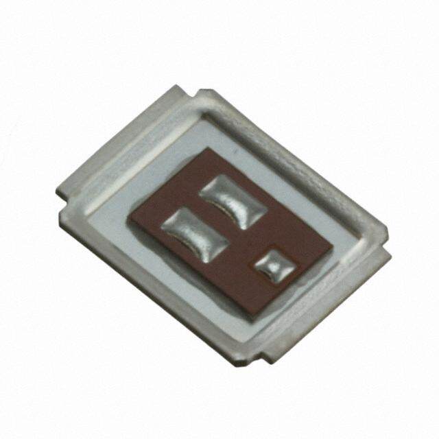
| 产品图片 |
|
| rohs | 符合RoHS无铅 / 符合限制有害物质指令(RoHS)规范要求 |
| 产品系列 | 晶体管,MOSFET,ROHM Semiconductor RRL025P03TR- |
| 数据手册 | |
| 产品型号 | RRL025P03TR |
| Pd-PowerDissipation | 1 W |
| Pd-功率耗散 | 1 W |
| Qg-GateCharge | 5.2 nC |
| Qg-栅极电荷 | 5.2 nC |
| RdsOn-Drain-SourceResistance | 55 mOhms |
| RdsOn-漏源导通电阻 | 55 mOhms |
| Vds-Drain-SourceBreakdownVoltage | 30 V |
| Vds-漏源极击穿电压 | - 30 V |
| Vgs-Gate-SourceBreakdownVoltage | +/- 20 V |
| Vgs-栅源极击穿电压 | 20 V |
| Vgsth-Gate-SourceThresholdVoltage | - 2.5 V |
| Vgsth-栅源极阈值电压 | - 2.5 V |
| 不同Id时的Vgs(th)(最大值) | 2.5V @ 1mA |
| 不同Vds时的输入电容(Ciss) | 480pF @ 10V |
| 不同Vgs时的栅极电荷(Qg) | 5.2nC @ 5V |
| 不同 Id、Vgs时的 RdsOn(最大值) | 75 毫欧 @ 2.5A,10V |
| 产品目录绘图 |
|
| 产品目录页面 | |
| 产品种类 | MOSFET |
| 供应商器件封装 | TUMT6 |
| 其它名称 | RRL025P03CT |
| 功率-最大值 | 1W |
| 包装 | 剪切带 (CT) |
| 商标 | ROHM Semiconductor |
| 安装类型 | 表面贴装 |
| 安装风格 | SMD/SMT |
| 导通电阻 | 55 mOhms |
| 封装 | Reel |
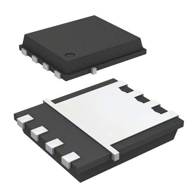
| 封装/外壳 | 6-SMD,扁平引线 |
| 封装/箱体 | TUMT-6 |
| 工厂包装数量 | 3000 |
| 晶体管极性 | P-Channel |
| 最大工作温度 | + 150 C |
| 最小工作温度 | - 55 C |
| 标准包装 | 1 |
| 汲极/源极击穿电压 | 30 V |
| 漏极连续电流 | 2.5 A |
| 漏源极电压(Vdss) | 30V |
| 特色产品 | http://www.digikey.com/cn/zh/ph/ROHM/MOSFET_ECOMOS.html |
| 电流-连续漏极(Id)(25°C时) | 2.5A (Ta) |
| 通道模式 | Enhancement |
| 配置 | Single |


- 商务部:美国ITC正式对集成电路等产品启动337调查
- 曝三星4nm工艺存在良率问题 高通将骁龙8 Gen1或转产台积电
- 太阳诱电将投资9.5亿元在常州建新厂生产MLCC 预计2023年完工
- 英特尔发布欧洲新工厂建设计划 深化IDM 2.0 战略
- 台积电先进制程称霸业界 有大客户加持明年业绩稳了
- 达到5530亿美元!SIA预计今年全球半导体销售额将创下新高
- 英特尔拟将自动驾驶子公司Mobileye上市 估值或超500亿美元
- 三星加码芯片和SET,合并消费电子和移动部门,撤换高东真等 CEO
- 三星电子宣布重大人事变动 还合并消费电子和移动部门
- 海关总署:前11个月进口集成电路产品价值2.52万亿元 增长14.8%


PDF Datasheet 数据手册内容提取
RRL025P03 Pch -30V -2.5A Power MOSFET Datasheet lOutline V -30V (6) DSS TUMT6 (5) R (Max.) 75mW (4) DS(on) I -2.5A D (1) (2) PD 1.0W (3) lFeatures lInner circuit 1) Low on - resistance. (1) Drain (2) Drain 2) Built-in G-S Protection Diode. (3) Gate (4) Source 3) Small Surface Mount Package (TUMT6). (5) Drain (6) Drain 4) Pb-free lead plating ; RoHS compliant *1 ESD PROTECTION DIODE *2 BODY DIODE lPackaging specifications Packaging Taping lApplication Reel size (mm) 180 Tape width (mm) 8 DC/DC converters Type Basic ordering unit (pcs) 3,000 Taping code TR Marking UA lAbsolute maximum ratings(T = 25°C) a Parameter Symbol Value Unit Drain - Source voltage V -30 V DSS Continuous drain current I *1 2.5 A D Pulsed drain current I *2 10 A D,pulse Gate - Source voltage V 20 V GSS P *3 1.0 W D Power dissipation P *4 0.32 W D Junction temperature T 150 °C j Range of storage temperature T -55 to +150 °C stg www.rohm.com © 2013 ROHM Co., Ltd. All rights reserved. 1/11 2013.02 - Rev.B
RRL025P03 Data Sheet lThermal resistance Values Parameter Symbol Unit Min. Typ. Max. R *3 - - 125 °C/W thJA Thermal resistance, junction - ambient R *4 - - 391 °C/W thJA lElectrical characteristics(T = 25°C) a Values Parameter Symbol Conditions Unit Min. Typ. Max. Drain - Source breakdown V V = 0V, I = -1mA -30 - - V voltage (BR)DSS GS D Breakdown voltage ΔV I = -1mA (BR)DSS D - -25 - mV/°C temperature coefficient ΔT referenced to 25°C j Zero gate voltage drain current I V = -30V, V = 0V - - -1 mA DSS DS GS Gate - Source leakage current I V = 20V, V = 0V - - 10 mA GSS GS DS Gate threshold voltage V V = -10V, I = -1mA -1 - -2.5 V GS (th) DS D Gate threshold voltage ΔV I = -1mA (GS)th D - 3.9 - mV/°C temperature coefficient ΔT referenced to 25°C j V = -10V, I = -2.5A - 55 75 GS D V = -4.5V, I = -1.2A - 85 115 Static drain - source GS D R *5 mW on - state resistance DS(on) V = -4.0V, I = -1.2A - 95 125 GS D V = -10V, I = -2.5A, T=125°C - 95 135 GS D j Gate input resistannce R f = 1MHz, open drain - 24 - W G Transconductance g *5 V = -10V, I = -2.5A 2.0 4.4 - S fs DS D *1 Limited only by maximum temperature allowed. *2 Pw 10ms, Duty cycle 1% *3 Mounted on a seramic board (30×30×0.8mm) *4 Mounted on a FR4 (15×20×0.8mm) *5 Pulsed www.rohm.com © 2013 ROHM Co., Ltd. All rights reserved. 2/11 2013.02 - Rev.B
RRL025P03 Data Sheet lElectrical characteristics(T = 25°C) a Values Parameter Symbol Conditions Unit Min. Typ. Max. Input capacitance C V = 0V - 480 - iss GS Output capacitance C V = -10V - 70 - pF oss DS Reverse transfer capacitance C f = 1MHz - 70 - rss Turn - on delay time t *5 V ⋍ -15V, V = -10V - 7 - d(on) DD GS Rise time t *5 I = -1.2A - 16 - r D ns Turn - off delay time t *5 R = 12.5W - 50 - d(off) L Fall time t *5 R = 10W - 33 - f G lGate Charge characteristics(T = 25°C) a Values Parameter Symbol Conditions Unit Min. Typ. Max. V ⋍ -15V, I = -2.5A DD D - 5.2 - V = -5V GS Total gate charge Q *5 g V ⋍ -15V, I = -2.5A DD D - 12 - nC V = -10V GS Gate - Source charge Qgs *5 VDD ⋍ -15V, ID= -2.5A - 1.6 - Gate - Drain charge Q *5 VGS = -5V - 1.6 - gd lBody diode electrical characteristics (Source-Drain)(T = 25°C) a Values Parameter Symbol Conditions Unit Min. Typ. Max. Inverse diode continuous, I *1 T = 25°C - - -0.8 A forward current S a Forward voltage V *5 V = 0V, I = -2.5A - - -1.2 V SD GS s www.rohm.com © 2013 ROHM Co., Ltd. All rights reserved. 3/11 2013.02 - Rev.B
RRL025P03 Data Sheet lElectrical characteristic curves Fig.1 Power Dissipation Derating Curve Fig.2 Maximum Safe Operating Area 120 100 Operation in this area P = 1ms %] is limited by RDS(on) W x. [ 100 10 ( VGS = 10V ) PW = 100ms a m 80 A] P D [D n : P/D 60 rent : -I 1 PW = 10ms atio 40 Cur DC Operation p n Dissi Drai 0.1 Ta=25ºC r 20 Single Pulse e Mounted on a ceramic board. w o (30mm × 30mm × 0.8mm) P 0 0.01 0 50 100 150 200 0.1 1 10 100 Junction Temperature : Tj [°C] Drain - Source Voltage : -V [V] DS Fig.3 Normalized Transient Thermal Fig.4 Single Pulse Maxmum Power Resistance vs. Pulse Width dissipation r(t) 10 1000 ce : TSain=g2l5eº CPu lse TSain=g2l5eº CPu lse an ) st 1 W si P( Re : 100 al top D=1 er m w r 0.1 D=0.5 o e D=0.1 P Th D=0.05 nt ent b o t t o m SDi=g0n.l0e1 nsie 10 si a n 0.01 r a Rth(ch-a)=125ºC/W T Tr Rth(ch-a)(t)=r(t)×Rth(ch-a) ak ed Mounted on ceramic board Pe z (30mm × 30mm × 0.8mm) ali 0.001 1 m r 0.0001 0.01 1 100 0.0001 0.01 1 100 o N Pulse Width : P [s] Pulse Width : P [s] W W www.rohm.com © 2013 ROHM Co., Ltd. All rights reserved. 4/11 2013.02 - Rev.B
RRL025P03 Data Sheet lElectrical characteristic curves Fig.5 Typical Output Characteristics(I) Fig.6 Typical Output Characteristics(II) 3 3 VGS= -10V Ta=25ºC 2.5 VGS= -4.5V 2.5 VGS= -10V Pulsed VGS= -3.8V VGS= -4.5V V = -3.6V -I [A] D 2 TPau=ls2e5dºC -I [A] D 2 VGS= -3.2GVS nt : 1.5 VGS= -3.2V nt : 1.5 VGS= -3.0V e e r r r r Cu VGS= -3.0V Cu n 1 n 1 ai V = -2.8V ai V = -2.8V r GS r GS D D 0.5 0.5 V = -2.5V GS 0 0 0 0.2 0.4 0.6 0.8 1 0 2 4 6 8 10 Drain - Source Voltage : -V [V] Drain - Source Voltage : -V [V] DS DS Fig.7 Breakdown Voltage Fig.8 Typical Transfer Characteristics vs. Junction Temperature V] 60 10 [SS VDS= -10V D Pulsed R) B V( e : - 40 A] 1 TTa== 17255ºCºC ag [D Ta= 25ºC n Volt nt : -I 0.1 Taa= -25ºC w e r do Cur k 20 a n re ai 0.01 B V = 0V r ce IDG =S -1mA D r u pulsed o S - 0 0.001 n -50 0 50 100 150 0 1 2 3 4 ai r D Junction Temperature : T [°C] Gate - Source Voltage : -V [V] j GS www.rohm.com © 2013 ROHM Co., Ltd. All rights reserved. 5/11 2013.02 - Rev.B
RRL025P03 Data Sheet lElectrical characteristic curves Fig.9 Gate Threshold Voltage Fig.10 Transconductance vs. Drain Current vs. Junction Temperature 3 10 V = -10V V] PDuSlsed [S(th) S] VG 2 [s - gf e : e : g c a n 1 eshold Volt 1 V = 10V nsconducta TTTTaaaa====271 -55225ºº5CCººC C hr DS a e T ID = -1mA Tr at pulsed G 0 0.1 -50 0 50 100 150 0.1 1 10 Junction Temperature : T [°C] Drain Current : -I [A] j D Fig.11 Drain CurrentDerating Curve Fig.12 Static Drain - Source On - State Resistance vs. Gate Source Voltage 1.2 300 e c T =25ºC n a 1 sta Pulsed n esi ID= -1.5A o R sipati%) 0.8 State W] 200 ID= -3.0A ain Current Dis: I/Imax. (DD 00..46 n - Source On-: R [mDS(on) 100 Dr 0.2 ai r D c 0 ati 0 -25 0 25 50 75 100 125 150 St 0 2 4 6 8 10 Junction Temperature : T [ºC] Gate - Source Voltage : -V [V] j GS www.rohm.com © 2013 ROHM Co., Ltd. All rights reserved. 6/11 2013.02 - Rev.B
RRL025P03 Data Sheet lElectrical characteristic curves Fig.13 Static Drain - Source On - State Fig.14 Static Drain - Source On - State Resistance vs. Drain Current(I) Resistance vs. Junction Temperature 1000 120 stance TPau=ls2e5dºC stance 100 VIpDuG =lSs =e- d2- .150AV si V = -4.0V si e GS e R V = -4.5V R e VGS= -10V e 80 StatW] GS StatW] -m -m n 100 n 60 e O [on) e O [on) c S( c S( r D r D uR uR 40 So: So: - - n n ai ai 20 r r D D c c ati 10 ati 0 St 0.1 1 10 St -50 -25 0 25 50 75 100 125 150 Drain Current : -I [A] Junction Temperature : T [ºC] D j Fig.15 Static Drain - Source On - State Fig.16 Static Drain-Source On-State Resistance vs. Drain Current(II) Resistance vs. Drain Current(III) esistance 1000 VPGuSls=e -d1 0V TTTaa===1722555ººCCºC Resistance 1000 VPGuSls=e -d4 .5V TTTaaa===1722555ººCCºC State RW] Taa= -25ºC -State Wm] Ta= -25ºC ce On- [mS(on) 100 rce On [DS(on) 100 r D uR ain - Sou: R rain - So: r D Static D 10 0.1 1 10 Static 10 0.1 1 10 Drain Current : -I [A] Drain Current : -I [A] D D www.rohm.com © 2013 ROHM Co., Ltd. All rights reserved. 7/11 2013.02 - Rev.B
RRL025P03 Data Sheet lElectrical characteristic curves Fig.17 Static Drain - Source On - State Fig.18 Typical Capacitance Resistance vs. Drain Current(IV) vs. Drain - Source Voltage e 1000 1000 anc VPGuSls=e -d4 .0V Ta=125ºC sist TTa==7255ººCC Re Ta= -25ºC Coss Ciss e a F] StatW] C [p -m Source On: R [DS(on) 100 acitance : 100 Crss n - Cap Ta=25ºC ai f=1MHz r D V =0V c GS ati 10 10 St 0.1 1 10 0.01 0.1 1 10 100 Drain Current : -I [A] Drain - Source Voltage : -V [V] D DS Fig.19 Switching Characteristics Fig.20 Dynamic Input Characteristics 1000 10 T =25ºC t a d(off) V = -15V DD VGS= -10V V] 8 ns] 100 tf RPuGl=s1e0dW -V [GS e : t [ age : 6 Tim Volt Switching 10 e - Source 24 TVIDaD==D 2=-52 -º.5C1A5 V tr td(on) at RG=10W G Pulsed 1 0 0.01 0.1 1 10 0 2 4 6 8 10 Drain Current : -I [A] Total Gate Charge : Q [nC] D g www.rohm.com © 2013 ROHM Co., Ltd. All rights reserved. 8/11 2013.02 - Rev.B
RRL025P03 Data Sheet lElectrical characteristic curves Fig.21 Source Current vs. Source Drain Voltage 10 V =0V GS Pulsed A] -I [S 1 TTa=a=17255ººCC nt : TT=a =-2255ººCC e a r r u C e 0.1 c r u o S 0.01 0 0.2 0.4 0.6 0.8 1 1.2 Source-Drain Voltage : -V [V] SD www.rohm.com © 2013 ROHM Co., Ltd. All rights reserved. 9/11 2013.02 - Rev.B
RRL025P03 Data Sheet lMeasurement circuits Fig.1-1 Switching Time Measurement Circuit Fig.1-2 Switching Waveforms Fig.2-1 Gate Charge Measurement Circuit Fig.2-2 Gate Charge Waveform www.rohm.com © 2013 ROHM Co., Ltd. All rights reserved. 10/11 2013.02 - Rev.B
RRL025P03 Data Sheet lDimensions (Unit : mm) D A TUMT6 e L E HE Lp b c x S A e 1 e 2 A A y S 1 l A1 S b2 Patterm of terminal position areas MILIMETERS INCHES DIM MIN MAX MIN MAX A - 0.85 - 0.033 A1 0.00 0.10 0 0.004 A2 0.72 0.82 0.028 0.032 b 0.25 0.40 0.01 0.016 c 0.12 0.22 0.005 0.009 D 1.90 2.10 0.075 0.083 E 1.60 1.80 0.063 0.071 e 0.65 0.03 HE 2.00 2.20 0.079 0.087 L 0.20 0.01 Lp - 0.40 - 0.016 x - 0.10 - 0.004 y - 0.10 - 0.004 MILIMETERS INCHES DIM MIN MAX MIN MAX e1 1.70 0.067 b2 - 0.50 - 0.02 l1 - 0.50 - 0.02 Dimension in mm/inches www.rohm.com © 2013 ROHM Co., Ltd. All rights reserved. 11/11 2013.02 - Rev.B
Notice Notes 1) The information contained herein is subject to change without notice. 2) Before you use our Products, please contact our sales representativeand verify the latest specifica- tions : 3) Although ROHM is continuously working to improve product reliability and quality, semicon- ductors can break down and malfunction due to various factors. Therefore, in order to prevent personal injury or fire arising from failure, please take safety measures such as complying with the derating characteristics, implementing redundant and fire prevention designs, and utilizing backups and fail-safe procedures. ROHM shall have no responsibility for any damages arising out of the use of our Poducts beyond the rating specified by ROHM. 4) Examples of application circuits, circuit constants and any other information contained herein are provided only to illustrate the standard usage and operations of the Products. The peripheral conditions must be taken into account when designing circuits for mass production. 5) The technical information specified herein is intended only to show the typical functions of and examples of application circuits for the Products. ROHM does not grant you, explicitly or implicitly, any license to use or exercise intellectual property or other rights held by ROHM or any other parties. ROHM shall have no responsibility whatsoever for any dispute arising out of the use of such technical information. 6) The Products are intended for use in general electronic equipment (i.e. AV/OA devices, communi- cation, consumer systems, gaming/entertainment sets) as well as the applications indicated in this document. 7) The Products specified in this document are not designed to be radiation tolerant. 8) For use of our Products in applications requiring a high degree of reliability (as exemplified below), please contact and consult with a ROHM representative : transportation equipment (i.e. cars, ships, trains), primary communication equipment, traffic lights, fire/crime prevention, safety equipment, medical systems, servers, solar cells, and power transmission systems. 9) Do not use our Products in applications requiring extremely high reliability, such as aerospace equipment, nuclear power control systems, and submarine repeaters. 10) ROHM shall have no responsibility for any damages or injury arising from non-compliance with the recommended usage conditions and specifications contained herein. 11) ROHM has used reasonable care to ensur the accuracy of the information contained in this document. However, ROHM does not warrants that such information is error-free, and ROHM shall have no responsibility for any damages arising from any inaccuracy or misprint of such information. 12) Please use the Products in accordance with any applicable environmental laws and regulations, such as the RoHS Directive. For more details, including RoHS compatibility, please contact a ROHM sales office. ROHM shall have no responsibility for any damages or losses resulting non-compliance with any applicable laws or regulations. 13) When providing our Products and technologies contained in this document to other countries, you must abide by the procedures and provisions stipulated in all applicable export laws and regulations, including without limitation the US Export Administration Regulations and the Foreign Exchange and Foreign Trade Act. 14) This document, in part or in whole, may not be reprinted or reproduced without prior consent of ROHM. Thank you for your accessing to ROHM product informations. More detail product informations and catalogs are available, please contact us. ROHM Customer Support System http://www.rohm.com/contact/ www.rohm.com R1102A © 2013 ROHM Co., Ltd. All rights reserved.
Mouser Electronics Authorized Distributor Click to View Pricing, Inventory, Delivery & Lifecycle Information: R OHM Semiconductor: RRL025P03TR