ICGOO在线商城 > 分立半导体产品 > 晶体管 - FET,MOSFET - 单 > AOT20N25L

 Datasheet下载
- 型号: AOT20N25L
- 制造商: ALPHA&OMEGA
- 库位|库存: xxxx|xxxx
- 要求:
| 数量阶梯 | 香港交货 | 国内含税 |
| +xxxx | $xxxx | ¥xxxx |
查看当月历史价格
查看今年历史价格
AOT20N25L产品简介:
ICGOO电子元器件商城为您提供AOT20N25L由ALPHA&OMEGA设计生产,在icgoo商城现货销售,并且可以通过原厂、代理商等渠道进行代购。 AOT20N25L价格参考¥10.92-¥10.92。ALPHA&OMEGAAOT20N25L封装/规格:晶体管 - FET,MOSFET - 单, 通孔 N 沟道 250V 20A(Tc) 208W(Tc) TO-220。您可以下载AOT20N25L参考资料、Datasheet数据手册功能说明书,资料中有AOT20N25L 详细功能的应用电路图电压和使用方法及教程。
AOT20N25L 是 Alpha & Omega Semiconductor Inc. 生产的一款 N 沟道增强型 MOSFET,主要应用于需要高效能和高可靠性的电源管理系统中。其典型应用场景包括:

1. 电源转换器:如DC-DC转换器、AC-DC电源适配器等,用于提高能量转换效率,降低损耗。

2. 电机驱动:在电动工具、电动车、工业电机控制中作为开关元件,实现对电机速度和方向的控制。

3. 负载开关:用于智能电源管理,控制设备中不同模块的供电通断,如笔记本电脑、服务器和通信设备中的电源管理。

4. 电池管理系统(BMS):在锂电池保护电路中作为充放电控制开关,确保电池安全运行。

5. 照明系统:如LED驱动电路中,用于调光和恒流控制。

该MOSFET具有低导通电阻、高耐压(250V)和较强电流承载能力(20A),适用于中高功率应用,且封装小巧,适合高密度电路设计。
| 参数 | 数值 |
| 产品目录 | |
| 描述 | MOSFET N-CH 250V 20A TO220 |
| 产品分类 | FET - 单 |
| FET功能 | 标准 |
| FET类型 | MOSFET N 通道,金属氧化物 |
| 品牌 | Alpha & Omega Semiconductor Inc |
| 数据手册 | |
| 产品图片 |
|
| 产品型号 | AOT20N25L |
| rohs | 无铅 / 符合限制有害物质指令(RoHS)规范要求 |
| 产品系列 | - |
| 不同Id时的Vgs(th)(最大值) | 4.5V @ 250µA |
| 不同Vds时的输入电容(Ciss) | 1028pF @ 25V |
| 不同Vgs时的栅极电荷(Qg) | 25nC @ 10V |
| 不同 Id、Vgs时的 RdsOn(最大值) | 170 毫欧 @ 10A,10V |
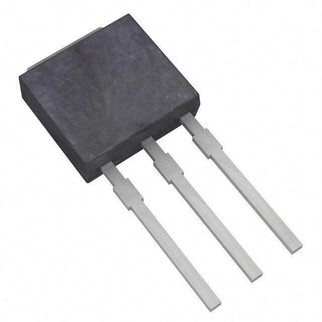
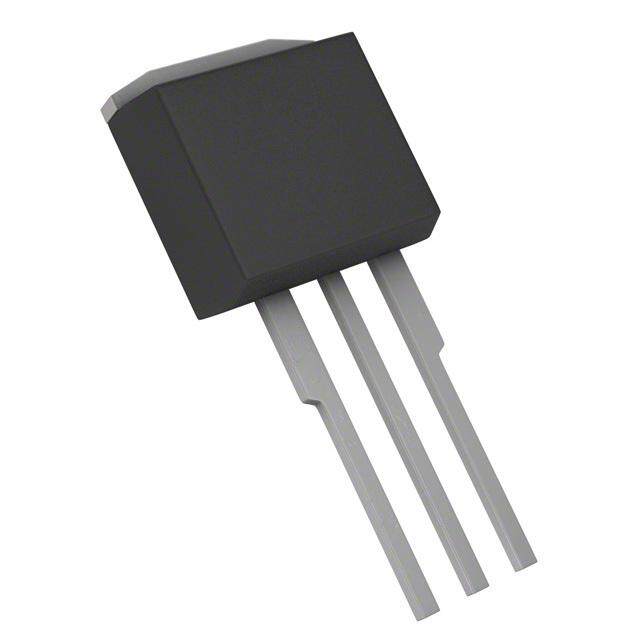
| 供应商器件封装 | TO-220 |
| 其它名称 | AOT20N25L-ND |
| 功率-最大值 | 208W |
| 包装 | 管件 |
| 安装类型 | 通孔 |
| 封装/外壳 | TO-220-3 |
| 标准包装 | 1,000 |
| 漏源极电压(Vdss) | 250V |
| 电流-连续漏极(Id)(25°C时) | 20A (Tc) |


- 商务部:美国ITC正式对集成电路等产品启动337调查
- 曝三星4nm工艺存在良率问题 高通将骁龙8 Gen1或转产台积电
- 太阳诱电将投资9.5亿元在常州建新厂生产MLCC 预计2023年完工
- 英特尔发布欧洲新工厂建设计划 深化IDM 2.0 战略
- 台积电先进制程称霸业界 有大客户加持明年业绩稳了
- 达到5530亿美元!SIA预计今年全球半导体销售额将创下新高
- 英特尔拟将自动驾驶子公司Mobileye上市 估值或超500亿美元
- 三星加码芯片和SET,合并消费电子和移动部门,撤换高东真等 CEO
- 三星电子宣布重大人事变动 还合并消费电子和移动部门
- 海关总署:前11个月进口集成电路产品价值2.52万亿元 增长14.8%


PDF Datasheet 数据手册内容提取
AOT20N25 250V,20A N-Channel MOSFET General Description Product Summary The AOT20N25 is fabricated using an advanced high VDS 300V@150℃ voltage MOSFET process that is designed to deliver high I (at V =10V) 20A D GS levels of performance and robustness in popular AC-DC R (at V =10V) < 0.17W DS(ON) GS applications.By providing low R , C and C along DS(on) iss rss with guaranteed avalanche capability this device can be adopted quickly into new and existing offline power supply designs.This device is ideal for boost converters and synchronous rectifiers for consumer, telecom, industrial 100% UIS Tested power supplies and LED backlighting. 100% R Tested g For Halogen Free add "L" suffix to part number: AOT20N25L Top View D TO-220 G S D G S Absolute Maximum Ratings T =25°C unless otherwise noted A PPaarraammeetteerr SSyymmbbooll AAOOTT2200NN2255 UUnniittss Drain-Source Voltage V 250 V DS Gate-Source Voltage V ±30 V GS Continuous Drain TC=25°C I 20 Current T =100°C D 14 A C Pulsed Drain Current C I 51 DM Avalanche Current C I 4.5 A AS Single pulsed avalanche energy G E 608 mJ AS Peak diode recovery dv/dt dv/dt 5 V/ns T =25°C 208 W C P Power Dissipation B Derate above 25oC D 1.7 W/ oC Junction and Storage Temperature Range T, T -55 to 150 °C J STG Maximum lead temperature for soldering purpose, 1/8" from case for 5 seconds TL 300 °C Thermal Characteristics Parameter Symbol AOT20N25 Units Maximum Junction-to-Ambient A,D RqJA 65 °C/W Maximum Case-to-sink A RqCS 0.5 °C/W Maximum Junction-to-Case RqJC 0.6 °C/W Rev0: Oct 2011 www.aosmd.com Page 1 of 5
AOT20N25 Electrical Characteristics (T =25°C unless otherwise noted) J Symbol Parameter Conditions Min Typ Max Units STATIC PARAMETERS I =250µA, V =0V, T=25°C 250 BV Drain-Source Breakdown Voltage D GS J DSS I =250µA, V =0V, T=150°C 300 V D GS J BV DSS Zero Gate Voltage Drain Current ID=250µA, VGS=0V 0.25 V/ oC /∆TJ V =250V, V =0V 1 IDSS Zero Gate Voltage Drain Current VDS=200V, TG=S125°C 10 m A DS J I Gate-Body leakage current V =0V, V =±30V ±100 nA GSS DS GS V Gate Threshold Voltage V =5V,I =250m A 3.2 3.8 4.5 V GS(th) DS D R Static Drain-Source On-Resistance V =10V, I =10A 0.14 0.17 W DS(ON) GS D g Forward Transconductance V =40V, I =10A 16 S FS DS D V Diode Forward Voltage I =1A,V =0V 0.72 1 V SD S GS I Maximum Body-Diode Continuous Current 20 A S I Maximum Body-Diode Pulsed Current 51 A SM DYNAMIC PARAMETERS C Input Capacitance 1028 pF iss C Output Capacitance V =0V, V =25V, f=1MHz 167 pF oss GS DS C Reverse Transfer Capacitance 11 pF rss R Gate resistance V =0V, V =0V, f=1MHz 1.9 3.9 5.9 W g GS DS SWITCHING PARAMETERS Q Total Gate Charge 20 25 nC g Q Gate Source Charge V =10V, V =200V, I =20A 5.7 nC gs GS DS D Q Gate Drain Charge 8 nC gd t Turn-On DelayTime 27 ns D(on) t Turn-On Rise Time V =10V, V =125V, I =20A, 31 ns r GS DS D ttDD((ooffff)) TTuurrnn--OOffff DDeellaayyTTiimmee RRGG==2255WW 7700 nnss t Turn-Off Fall Time 25 ns f trr Body Diode Reverse Recovery Time IF=20A,dI/dt=100A/m s,VDS=100V 179 ns Qrr Body Diode Reverse Recovery Charge IF=20A,dI/dt=100A/m s,VDS=100V 1.6 m C A. The value of RqJAis measured with the device in a still air environment with TA =25°C. B. The power dissipation P is based on T =150°C, using junction-to-case thermal resistance, and is more useful in setting the upper D J(MAX) dissipation limit for cases where additional heatsinking is used. C. Repetitive rating, pulse width limited by junction temperature T =150°C, Ratings are based on low frequency and duty cycles to keep initial J(MAX) T =25°C. J D. The RqJAis the sum of the thermal impedance from junction to case RqJCand case to ambient. E. The static characteristics in Figures 1 to 6 are obtained using <300 m s pulses, duty cycle 0.5% max. F. These curves are based on the junction-to-case thermal impedance which is measured with the device mounted to a large heatsink, assuming a maximum junction temperature of T =150°C. The SOA curve provides a single pulse rating. J(MAX) G. L=60mH, I =4.5A, V =150V, R =25Ω, Starting T=25°C AS DD G J THIS PRODUCT HAS BEEN DESIGNED AND QUALIFIED FOR THE CONSUMER MARKET. APPLICATIONS OR USES AS CRITICAL COMPONENTS IN LIFE SUPPORT DEVICES OR SYSTEMS ARE NOT AUTHORIZED. AOS DOES NOT ASSUME ANY LIABILITY ARISING OUT OF SUCH APPLICATIONS OR USES OF ITS PRODUCTS. AOS RESERVES THE RIGHT TO IMPROVE PRODUCT DESIGN, FUNCTIONS AND RELIABILITY WITHOUT NOTICE. Rev0: Oct 2011 www.aosmd.com Page 2 of 5
AOT20N25 TYPICAL ELECTRICAL AND THERMAL CHARACTERISTICS 30 100 10V VDS=40V -55°C 25 6.5V 125°C 20 10 I(A)D 15 6V I(A)D 10 1 25°C 5 V =5.5V GS 0 0.1 0 5 10 15 20 25 30 2 4 6 8 10 Fig 1: On-RVeDgSio(nV oClthsa)racteristics Figure 2: TraVnGsSf(eVro Clths)aracteristics 0.30 3 e 0.25 nc 2.5 VGS=10V VGS=10V sta ID=10A 0.20 esi 2 ) R W( n- N) 0.15 O 1.5 RDS(O 0.10 alized 1 m or 0.05 N 0.5 0.00 0 0 5 10 15 20 25 -100 -50 0 50 100 150 200 I (A) Temperature (°C) FFiigguurree 33:: OOnn--RReessiissttaanncceeD vvss.. DDrraaiinn CCuurrrreenntt aanndd GGaattee Figure 4: On-Resistance vs. Junction Temperature Voltage 1.2 1E+02 1E+01 d) 1.1 ze 40 125°C ali 1E+00 m A) or ( (N 1 IS 1E-01 25°C S S D V B 1E-02 0.9 1E-03 0.8 1E-04 -100 -50 0 50 100 150 200 0.2 0.4 0.6 0.8 1.0 Figure 5:Break DownT Jv (s°. JCu)nction Temperature Figure 6: Body-DioVdSDe (CVhoaltrsa)cteristics (Note E) Rev0: Oct 2011 www.aosmd.com Page 3 of 5
AOT20N25 TYPICAL ELECTRICAL AND THERMAL CHARACTERISTICS 15 10000 V =200V 12 ID=S20A Ciss D 1000 F) p s) 9 e ( (VoltS citanc 100 Coss G 6 a V p a C 10 3 C rss 0 1 0 5 10 15 20 25 30 35 0.1 1 10 100 Figure 7: Gate-CQhga(rngCe) Characteristics Figure 8: CapaVcDiSta(Vncoelt sC)haracteristics 100 25 10m s R DS(ON) 20 10 limited 100m s A) (D ng I 15 ps) DC 1ms ent rati 10 I(AmD 1 10ms urr C 0.1 5 T =150°C J(Max) 0 0.01 0 25 50 75 100 125 150 0.1 1 10 100 1000 TT ((°°CC)) VV ((VVoollttss)) CCAASSEE DDSS Figure 9: Current De-rating (Note B) Figure 10: Maximum Forward Biased Safe Operating Area for AOT20N25 (Note F) 10 D=T /T In descending order on nsient nce 1 TRJq,JPCK==0T.C6+°PCDM/W.ZqJC.RqJC D=0.5, 0.3, 0.1, 0.05, 0.02, 0.01, single pulse Trasta d si ee zR 0.1 malimal PD Norher ZqJCT 0.01 Single Pulse Ton T 0.001 1E-06 1E-05 0.0001 0.001 0.01 0.1 1 10 Pulse Width (s) Figure 11: Normalized Maximum Transient Thermal Impedance for AOT20N25 (Note F) Rev0: Oct 2011 www.aosmd.com Page 4 of 5
AOT20N25 Gate Charge Test Circuit & Waveform Vgs Qg + 10V + VDC Qgs Qgd - Vds VDC - DUT Vgs Ig Charge Resistive Switching Test Circuit & Waveforms RL Vds Vds 90% + Vgs DUT Vdd VDC Rg - 10% Vgs Vgs td(on) tr td(off) tf ton toff Unclamped Inductive Switching (UIS) Test Circuit & Waveforms L 2 Vds E A R = 1/2 LI AR BVDSS Id Vds ++ VVggss Vgs VDC Vdd IAR Rg - Id DUT Vgs Vgs Diode Recovery Test Circuit & Waveforms Vds + Q r r = - Idt DUT Vgs Vds - L Isd I t Isd F dI/dt rr + I Vgs VDC Vdd RM Vdd - Vds Ig Rev0: Oct 2011 www.aosmd.com Page 5 of 5