ICGOO在线商城 > 分立半导体产品 > 晶体管 - FET,MOSFET - 单 > STP20N65M5
 Datasheet下载
- 型号: STP20N65M5
- 制造商: STMicroelectronics
- 库位|库存: xxxx|xxxx
- 要求:
| 数量阶梯 | 香港交货 | 国内含税 |
| +xxxx | $xxxx | ¥xxxx |
查看当月历史价格
查看今年历史价格
STP20N65M5产品简介:
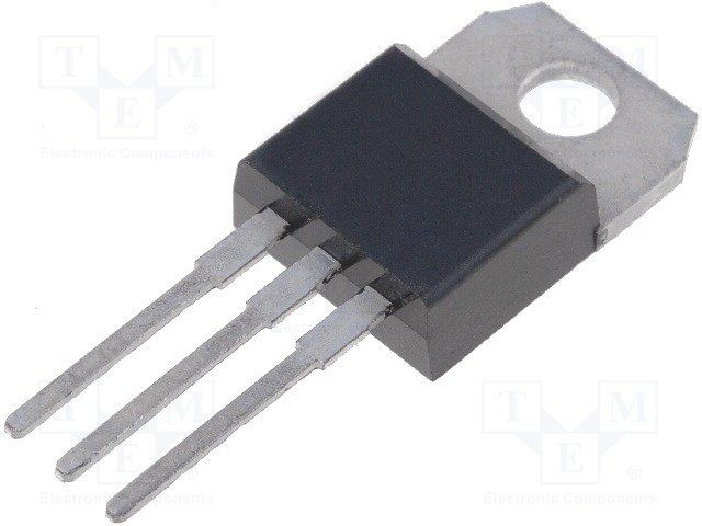
ICGOO电子元器件商城为您提供STP20N65M5由STMicroelectronics设计生产,在icgoo商城现货销售,并且可以通过原厂、代理商等渠道进行代购。 STP20N65M5价格参考。STMicroelectronicsSTP20N65M5封装/规格:晶体管 - FET,MOSFET - 单, 通孔 N 沟道 650V 18A(Tc) 130W(Tc) TO-220。您可以下载STP20N65M5参考资料、Datasheet数据手册功能说明书,资料中有STP20N65M5 详细功能的应用电路图电压和使用方法及教程。
STP20N65M5 是 STMicroelectronics(意法半导体)生产的一款 N 沟道增强型 MOSFET,属于晶体管 - FET、MOSFET - 单类别的产品。其主要应用场景包括:

1. 开关电源 (SMPS)
   STP20N65M5 适用于各种开关电源设计,例如 DC-DC 转换器和 AC-DC 适配器。其低导通电阻 (Rds(on)) 和高击穿电压 (650V) 特性使其能够在高压环境下高效工作,适合用于功率因数校正 (PFC) 电路或同步整流应用。

2. 电机驱动
   该器件可用于工业和消费类电机驱动应用中,如家用电器(风扇、泵、空调压缩机等)的无刷直流电机 (BLDC) 驱动器。其高耐压能力能够承受电机启动时的瞬态电压尖峰。

3. 逆变器
   在太阳能逆变器或 UPS 系统中,STP20N65M5 可作为主开关元件使用。它支持高频开关操作,并且具有良好的动态性能,有助于提高系统的效率和可靠性。

4. 负载切换与保护
   该 MOSFET 可用作负载切换开关,在汽车电子、工业控制和其他需要快速启停的应用中实现过流保护、短路保护等功能。

5. 电动工具
   对于需要高功率输出的电动工具(如电钻、割草机等),STP20N65M5 提供了足够的电流承载能力和耐用性,同时保持较低的功耗。

6. LED 驱动器
   在大功率 LED 照明系统中,这款 MOSFET 可用于恒流驱动电路,确保 LED 的稳定亮度并延长使用寿命。

总之,STP20N65M5 凭借其优异的电气特性和稳定性,广泛应用于需要高效功率转换、高压处理以及可靠开关功能的各种领域。
| 参数 | 数值 |
| 产品目录 | |
| 描述 | MOSFET N-CH 650V 18A TO-220MOSFET N-Ch 650V 0.168 Ohm 18A Mdmesh V |
| 产品分类 | FET - 单分离式半导体 |
| FET功能 | 标准 |
| FET类型 | MOSFET N 通道,金属氧化物 |
| Id-ContinuousDrainCurrent | 18 A |
| Id-连续漏极电流 | 18 A |
| 品牌 | STMicroelectronics |
| 产品手册 | |
| 产品图片 |
|
| rohs | 符合RoHS无铅 / 符合限制有害物质指令(RoHS)规范要求 |
| 产品系列 | 晶体管,MOSFET,STMicroelectronics STP20N65M5MDmesh™ V |
| 数据手册 | |
| 产品型号 | STP20N65M5 |
| Pd-PowerDissipation | 130 W |
| Pd-功率耗散 | 130 W |
| Qg-GateCharge | 36 nC |
| Qg-栅极电荷 | 36 nC |
| RdsOn-Drain-SourceResistance | 190 mOhms |
| RdsOn-漏源导通电阻 | 190 mOhms |
| Vds-Drain-SourceBreakdownVoltage | 650 V |
| Vds-漏源极击穿电压 | 650 V |
| Vgs-Gate-SourceBreakdownVoltage | +/- 25 V |
| Vgs-栅源极击穿电压 | 25 V |
| Vgsth-Gate-SourceThresholdVoltage | 4 V |
| Vgsth-栅源极阈值电压 | 4 V |
| 上升时间 | 7.5 ns |
| 下降时间 | 7.5 ns |
| 不同Id时的Vgs(th)(最大值) | 5V @ 250µA |
| 不同Vds时的输入电容(Ciss) | 1345pF @ 100V |
| 不同Vgs时的栅极电荷(Qg) | 45nC @ 10V |
| 不同 Id、Vgs时的 RdsOn(最大值) | 190 毫欧 @ 9A,10V |
| 产品种类 | MOSFET |
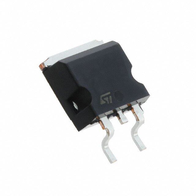
| 供应商器件封装 | TO-220 |
| 其它名称 | 497-13538 |
| 其它有关文件 | http://www.st.com/web/catalog/sense_power/FM100/CL824/SC1167/PF253456?referrer=70071840 |
| 功率-最大值 | 130W |
| 包装 | 管件 |
| 商标 | STMicroelectronics |
| 安装类型 | 通孔 |
| 安装风格 | Through Hole |
| 封装 | Tube |
| 封装/外壳 | TO-220-3 |
| 封装/箱体 | TO-220-3 |
| 工厂包装数量 | 50 |
| 晶体管极性 | N-Channel |
| 标准包装 | 50 |
| 漏源极电压(Vdss) | 650V |
| 电流-连续漏极(Id)(25°C时) | 18A (Tc) |
| 系列 | STP20N65M5 |


- 商务部:美国ITC正式对集成电路等产品启动337调查
- 曝三星4nm工艺存在良率问题 高通将骁龙8 Gen1或转产台积电
- 太阳诱电将投资9.5亿元在常州建新厂生产MLCC 预计2023年完工
- 英特尔发布欧洲新工厂建设计划 深化IDM 2.0 战略
- 台积电先进制程称霸业界 有大客户加持明年业绩稳了
- 达到5530亿美元!SIA预计今年全球半导体销售额将创下新高
- 英特尔拟将自动驾驶子公司Mobileye上市 估值或超500亿美元
- 三星加码芯片和SET,合并消费电子和移动部门,撤换高东真等 CEO
- 三星电子宣布重大人事变动 还合并消费电子和移动部门
- 海关总署:前11个月进口集成电路产品价值2.52万亿元 增长14.8%


PDF Datasheet 数据手册内容提取
STB20N65M5, STI20N65M5, STP20N65M5, STW20N65M5 Ω N-channel 650 V, 0.160 typ., 18 A MDmesh™ V Power MOSFET 2 2 in D PAK, I PAK, TO-220 and TO-247 packages Datasheet — production data Features TAB TAB V @ R Order codes DS DS(on) I T max D 2 Jmax STB20N65M5 1 3 123 STI20N65M5 D2PAK I2PAK 710 V 0.19 Ω 18 A STP20N65M5 TAB STW20N65M5 ■ Worldwide best R * area DS(on) 3 ■ Higher V rating and high dv/dt capability 2 3 DSS 1 2 1 ■ Excellent switching performance TO-220 TO-247 ■ 100% avalanche tested Figure 1. Internal schematic diagram Applications ■ Switching applications (cid:36)(cid:8)(cid:18)(cid:12)(cid:0)(cid:52)(cid:33)(cid:34)(cid:9) Description These devices are N-channel MDmesh™ V Power MOSFETs based on an innovative (cid:39)(cid:8)(cid:17)(cid:9) proprietary vertical process technology, which is combined with STMicroelectronics’ well-known PowerMESH™ horizontal layout structure. The resulting product has extremely low on- (cid:51)(cid:8)(cid:19)(cid:9) resistance, which is unmatched among silicon- based Power MOSFETs, making it especially (cid:33)(cid:45)(cid:16)(cid:17)(cid:20)(cid:23)(cid:21)(cid:86)(cid:17) suitable for applications which require superior power density and outstanding efficiency. Table 1. Device summary Order codes Marking Package Packaging STB20N65M5 D2PAK Tape and reel STI20N65M5 I2PAK 20N65M5 STP20N65M5 TO-220 Tube STW20N65M5 TO-247 February 2013 Doc ID 022865 Rev 2 1/21 This is information on a product in full production. www.st.com 21
Contents STB20N65M5, STI20N65M5, STP20N65M5, STW20N65M5 Contents 1 Electrical ratings . . . . . . . . . . . . . . . . . . . . . . . . . . . . . . . . . . . . . . . . . . . . 3 2 Electrical characteristics . . . . . . . . . . . . . . . . . . . . . . . . . . . . . . . . . . . . . 4 2.1 Electrical characteristics (curves) . . . . . . . . . . . . . . . . . . . . . . . . . . . . . . 6 3 Test circuits . . . . . . . . . . . . . . . . . . . . . . . . . . . . . . . . . . . . . . . . . . . . . . 9 4 Package mechanical data . . . . . . . . . . . . . . . . . . . . . . . . . . . . . . . . . . . . 10 5 Packaging mechanical data . . . . . . . . . . . . . . . . . . . . . . . . . . . . . . . . . . 18 6 Revision history . . . . . . . . . . . . . . . . . . . . . . . . . . . . . . . . . . . . . . . . . . . 20 2/21 Doc ID 022865 Rev 2
STB20N65M5, STI20N65M5, STP20N65M5, STW20N65M5 Electrical ratings 1 Electrical ratings T able 2. Absolute maximum ratings Symbol Parameter Value Unit V Gate-source voltage ± 25 V GS I Drain current (continuous) at T = 25 °C 18 A D C I Drain current (continuous) at T = 100 °C 11.3 A D C I (1) Drain current (pulsed) 72 A DM P Total dissipation at T = 25 °C 130 W TOT C dv/dt (1) Peak diode recovery voltage slope 15 V/ns T Storage temperature - 55 to 150 °C stg T Max. operating junction temperature 150 °C j 1. I ≤ 18 A, di/dt ≤ 400 A/µs; V peak < V , V =400 V SD DS (BR)DSS DD T able 3. Thermal data Value Symbol Parameter I2PAK, Unit D2PAK TO-247 TO-220 R Thermal resistance junction-case max 0.96 °C/W thj-case R Thermal resistance junction-ambient max 62.5 50 °C/W thj-amb R (1) Thermal resistance junction-pcb max 30 °C/W thj-pcb 1. When mounted on 1 inch² FR-4, 1 Oz copper board. T able 4. Avalanche characteristics Symbol Parameter Value Unit Avalanche current, repetetive or not I 4 A AR repetetive (pulse width limited by T ) jmax Single pulse avalanche energy (starting E 270 mJ AS t=25°C, I = I ; V =50 V) j d AR dd Doc ID 022865 Rev 2 3/21
Electrical characteristics STB20N65M5, STI20N65M5, STP20N65M5, STW20N65M5 2 Electrical characteristics (T = 25 °C unless otherwise specified) C Table 5. On /off states Symbol Parameter Test conditions Min. Typ. Max. Unit Drain-source V I = 1 mA, V = 0 650 V (BR)DSS breakdown voltage D GS Zero gate voltage V = 650 V 1 µA I DS DSS drain current (V = 0) V = 650 V, T =125 °C 100 µA GS DS C Gate-body leakage I V = ± 25 V ± 100 nA GSS current (V = 0) GS DS V Gate threshold voltage V = V , I = 250 µA 3 4 5 V GS(th) DS GS D Static drain-source R V = 10 V, I = 9 A 0.160 0.19 Ω DS(on) on-resistance GS D Table 6. Dynamic Symbol Parameter Test conditions Min. Typ. Max. Unit Input capacitance C 1434 pF Ciss Output capacitance VDS = 100 V, f = 1 MHz, - 38 - pF Coss Reverse transfer VGS = 0 3.7 pF rss capacitance Equivalent C (1) capacitance time - 118 - pF o(tr) related V = 0 to 520 V, V = 0 DS GS Equivalent C (2) capacitance energy - 35 - pF o(er) related Intrinsic gate R f = 1 MHz open drain - 3.5 - Ω G resistance Q Total gate charge V = 520 V, I = 9 A, 36 nC g DD D Q Gate-source charge V = 10 V - 7.5 - nC gs GS Q Gate-drain charge (see Figure18) 18 nC gd 1. Time related is defined as a constant equivalent capacitance giving the same charging time as C when oss V increases from 0 to 80% V DS DSS 2. Energy related is defined as a constant equivalent capacitance giving the same stored energy as C oss when V increases from 0 to 80% V DS DSS 4/21 Doc ID 022865 Rev 2
STB20N65M5, STI20N65M5, STP20N65M5, STW20N65M5 Electrical characteristics Table 7. Switching times Symbol Parameter Test conditions Min. Typ. Max Unit td(v) Voltage delay time VDD = 400 V, ID = 12 A, 43 ns tr(v) Voltage rise time RG = 4.7 Ω, VGS = 10 V - 7.5 - ns tf(i) Current fall time (see Figure19 and 7.5 ns t Crossing time Figure22) 11.5 ns c(off) Table 8. Source drain diode Symbol Parameter Test conditions Min. Typ. Max. Unit I Source-drain current 18 A SD - I (1) Source-drain current (pulsed) 72 A SDM V (2) Forward on voltage I = 18 A, V = 0 - 1.5 V SD SD GS t Reverse recovery time 288 ns rr I = 18 A, di/dt = 100 A/µs Q Reverse recovery charge SD - 4 µC rr V = 100 V (see Figure22) I Reverse recovery current DD 27 A RRM t Reverse recovery time I = 18 A, di/dt = 100 A/µs 342 ns rr SD Q Reverse recovery charge V = 100 V, T = 150 °C - 4.7 µC rr DD j I Reverse recovery current (see Figure22) 28 A RRM 1. Pulse width limited by safe operating area. 2. Pulsed: pulse duration = 300 µs, duty cycle 1.5% Doc ID 022865 Rev 2 5/21
Electrical characteristics STB20N65M5, STI20N65M5, STP20N65M5, STW20N65M5 2.1 Electrical characteristics (curves) Figure 2. Safe operating area for D²PAK, Figure 3. Thermal impedance for D²PAK, I²PAK, TO-220 I²PAK, TO-220 ID AM15584v1 (A) 10 Operatimiotne id n btyh ism aarx eaR iDsS(on) 11000µµss Li 1ms 1 Tj=150°C Tc=25°C 10ms Single pulse 0.1 0.1 1 10 100 VDS(V) Figure 4. S afe operating area for TO-247 Figure 5. Thermal impedance for TO-247 ID AM15586v1 (A) 10 Operatimiotne id n btyh ism aarx eaR iDsS(on) 11000µµss Li 1ms 1 Tj=150°C Tc=25°C 10ms Single pulse 0.1 0.1 1 10 100 VDS(V) Figure 6. O utput characteristics Figure 7. Transfer characteristics AM15587v1 AM15588v1 ID ID (A) VGS= 9, 10 V (A) 40 40 VDS= 25 V 35 35 VGS= 8 V 30 30 25 25 20 VGS= 7 V 20 15 15 10 10 5 VGS= 6 V 5 0 0 0 5 10 15 20 25VDS(V) 3 4 5 6 7 8 9 VGS(V) 6/21 Doc ID 022865 Rev 2
STB20N65M5, STI20N65M5, STP20N65M5, STW20N65M5 Electrical characteristics Figure 8. Gate charge vs gate-source voltage Figure 9. Static drain-source on-resistance VGS AM15589v1 RDS(on) AM15590v1 (V) VDS (Ω) VDS VDD=520V (V) 0.195 12 ID=9A 500 VGS=10V 0.185 10 400 0.175 8 300 0.165 6 0.155 200 4 0.145 2 100 0.135 0 0 0.125 0 10 20 30 40 Qg(nC) 0 5 10 15 ID(A) Figure 10. Capacitance variations Figure 11. Output capacitance stored energy C AM15591v1 Eoss AM15592v1 (pF) (µJ) 7 10000 6 Ciss 5 1000 4 100 3 Coss 2 10 1 Crss 1 0 0.1 1 10 100 VDS(V) 0 100 200 300 400 500 600 VDS(V) Figure 12. Normalized gate threshold voltage Figure 13. Normalized on-resistance vs vs temperature temperature VGS(th) AM05459v1 RDS(on) AM05460v1 (norm) (norm) 1.10 2.1 ID = 250 µA VGS= 10V VDS = VGS 1.9 ID= 9 A 1.00 1.7 1.5 0.90 1.3 1.1 0.80 0.9 0.7 0.70 0.5 -50 -25 0 25 50 75 100 TJ(°C) -50 -25 0 25 50 75 100 TJ(°C) Doc ID 022865 Rev 2 7/21
Electrical characteristics STB20N65M5, STI20N65M5, STP20N65M5, STW20N65M5 Figure 14. Normalized B vs temperature Figure 15. Drain-source diode forward VDSS characteristics VDS AM10399v1 VSD AM05461v1 (norm) (V) TJ=-50°C 1.08 ID = 1mA 1.2 1.06 1.0 1.04 1.02 0.8 TJ=25°C 1.00 0.6 0.98 TJ=150°C 0.4 0.96 0.2 0.94 0.92 0 -50 -25 0 25 50 75 100 TJ(°C) 0 10 20 30 40 50 ISD(A) Figure 16. S witching losses vs gate resistance (1) AM15593v1 E(μJ) VDD=400V Eon 250 VGS=10V ID=12A 200 150 Eoff 100 50 0 0 10 20 30 40 RG(Ω) 1. Eon including reverse recovery of a SiC diode 8/21 Doc ID 022865 Rev 2
STB20N65M5, STI20N65M5, STP20N65M5, STW20N65M5 Test circuits 3 Test circuits Figure 17. Switching times test circuit for Figure 18. Gate charge test circuit resistive load (cid:54)(cid:36)(cid:36) (cid:17)(cid:18)(cid:54) (cid:20)(cid:23)(cid:75) (cid:17)(cid:75) (cid:17)(cid:16)(cid:16)(cid:78)(cid:38) (cid:50)(cid:44) (cid:18)(cid:18)(cid:16)(cid:16) (cid:19)(cid:14)(cid:19) (cid:38) (cid:38) (cid:54)(cid:36)(cid:36) (cid:41)(cid:39)(cid:29)(cid:35)(cid:47)(cid:46)(cid:51)(cid:52) (cid:54)(cid:36) (cid:54)(cid:73)(cid:29)(cid:18)(cid:16)(cid:54)(cid:29)(cid:54)(cid:39)(cid:45)(cid:33)(cid:56) (cid:17)(cid:16)(cid:16) (cid:36)(cid:14)(cid:53)(cid:14)(cid:52)(cid:14) (cid:54)(cid:39)(cid:51) (cid:18)(cid:18)(cid:16)(cid:16) (cid:50)(cid:39) (cid:36)(cid:14)(cid:53)(cid:14)(cid:52)(cid:14) (cid:38) (cid:18)(cid:14)(cid:23)(cid:75) (cid:54)(cid:39) (cid:48)(cid:55) (cid:20)(cid:23)(cid:75) (cid:17)(cid:75) (cid:48)(cid:55) (cid:33)(cid:45)(cid:16)(cid:17)(cid:20)(cid:22)(cid:24)(cid:86)(cid:17) (cid:33)(cid:45)(cid:16)(cid:17)(cid:20)(cid:22)(cid:25)(cid:86)(cid:17) Figure 19. Test circuit for inductive load Figure 20. Unclamped inductive load test switching and diode recovery times circuit (cid:44) (cid:33) (cid:33) (cid:33) (cid:36) (cid:38)(cid:33)(cid:51)(cid:52) (cid:44)(cid:29)(cid:17)(cid:16)(cid:16) (cid:40) (cid:54)(cid:36) (cid:39) (cid:36)(cid:14)(cid:53)(cid:14)(cid:52)(cid:14) (cid:36)(cid:41)(cid:47)(cid:36)(cid:37) (cid:18)(cid:18)(cid:16)(cid:16) (cid:19)(cid:14)(cid:19) (cid:38) (cid:38) (cid:54)(cid:36)(cid:36) (cid:51) (cid:34) (cid:19)(cid:14)(cid:19) (cid:17)(cid:16)(cid:16)(cid:16) (cid:34) (cid:34) (cid:38) (cid:38) (cid:18)(cid:21) (cid:36) (cid:54)(cid:36)(cid:36) (cid:41)(cid:36) (cid:39) (cid:50)(cid:39) (cid:51) (cid:54)(cid:73) (cid:36)(cid:14)(cid:53)(cid:14)(cid:52)(cid:14) (cid:48)(cid:87) (cid:33)(cid:45)(cid:16)(cid:17)(cid:20)(cid:23)(cid:16)(cid:86)(cid:17) (cid:33)(cid:45)(cid:16)(cid:17)(cid:20)(cid:23)(cid:17)(cid:86)(cid:17) Figure 21. Unclamped inductive waveform Figure 22. Switching time waveform (cid:54)(cid:8)(cid:34)(cid:50)(cid:9)(cid:36)(cid:51)(cid:51) Inductive Load Turn-off Id (cid:54)(cid:36) 90%Vds 90%Id td(v) (cid:41)(cid:36)(cid:45) Vgs 90%Vgs oonn (cid:41)(cid:36) Vgs(I(t)))) (cid:54)(cid:36)(cid:36) (cid:54)(cid:36)(cid:36) 10%Vds 10%Id Vds tr(v) tf(i) (cid:33)(cid:45)(cid:16)(cid:17)(cid:20)(cid:23)(cid:18)(cid:86)(cid:17) tc(off) AM05540v1 Doc ID 022865 Rev 2 9/21
Package mechanical data STB20N65M5, STI20N65M5, STP20N65M5, STW20N65M5 4 Package mechanical data In order to meet environmental requirements, ST offers these devices in different grades of ECOPACK® packages, depending on their level of environmental compliance. ECOPACK® specifications, grade definitions and product status are available at: www.st.com. ECOPACK® is an ST trademark. 10/21 Doc ID 022865 Rev 2
STB20N65M5, STI20N65M5, STP20N65M5, STW20N65M5 Package mechanical data Table 9. D²PAK (TO-263) mechanical data mm Dim. Min. Typ. Max. A 4.40 4.60 A1 0.03 0.23 b 0.70 0.93 b2 1.14 1.70 c 0.45 0.60 c2 1.23 1.36 D 8.95 9.35 D1 7.50 E 10 10.40 E1 8.50 e 2.54 e1 4.88 5.28 H 15 15.85 J1 2.49 2.69 L 2.29 2.79 L1 1.27 1.40 L2 1.30 1.75 R 0.4 V2 0° 8° Doc ID 022865 Rev 2 11/21
Package mechanical data STB20N65M5, STI20N65M5, STP20N65M5, STW20N65M5 Figure 23. D²PAK (TO-263) drawing 0079457_T Figure 24. D²PAK footprint(a) 16.90 12.20 5.08 1.60 3.50 9.75 Footprint a. All dimension are in millimeters 12/21 Doc ID 022865 Rev 2
STB20N65M5, STI20N65M5, STP20N65M5, STW20N65M5 Package mechanical data Table 10. I²PAK (TO-262) mechanical data mm. DIM. min. typ max. A 4.40 4.60 A1 2.40 2.72 b 0.61 0.88 b1 1.14 1.70 c 0.49 0.70 c2 1.23 1.32 D 8.95 9.35 e 2.40 2.70 e1 4.95 5.15 E 10 10.40 L 13 14 L1 3.50 3.93 L2 1.27 1.40 Figure 25. I²PAK (TO-262) drawing 0004982_Rev_H Doc ID 022865 Rev 2 13/21
Package mechanical data STB20N65M5, STI20N65M5, STP20N65M5, STW20N65M5 Table 11. TO-220 type A mechanical data mm Dim. Min. Typ. Max. A 4.40 4.60 b 0.61 0.88 b1 1.14 1.70 c 0.48 0.70 D 15.25 15.75 D1 1.27 E 10 10.40 e 2.40 2.70 e1 4.95 5.15 F 1.23 1.32 H1 6.20 6.60 J1 2.40 2.72 L 13 14 L1 3.50 3.93 L20 16.40 L30 28.90 ∅ P 3.75 3.85 Q 2.65 2.95 14/21 Doc ID 022865 Rev 2
STB20N65M5, STI20N65M5, STP20N65M5, STW20N65M5 Package mechanical data Figure 26. TO-220 type A drawing 0015988_typeA_Rev_S Doc ID 022865 Rev 2 15/21
Package mechanical data STB20N65M5, STI20N65M5, STP20N65M5, STW20N65M5 Table 12. TO-247 mechanical data mm. Dim. Min. Typ. Max. A 4.85 5.15 A1 2.20 2.60 b 1.0 1.40 b1 2.0 2.40 b2 3.0 3.40 c 0.40 0.80 D 19.85 20.15 E 15.45 15.75 e 5.30 5.45 5.60 L 14.20 14.80 L1 3.70 4.30 L2 18.50 ∅P 3.55 3.65 ∅R 4.50 5.50 S 5.30 5.50 5.70 16/21 Doc ID 022865 Rev 2
STB20N65M5, STI20N65M5, STP20N65M5, STW20N65M5 Package mechanical data Figure 27. TO-247 drawing 0075325_G Doc ID 022865 Rev 2 17/21
Packaging mechanical data STB20N65M5, STI20N65M5, STP20N65M5, STW20N65M5 5 Packaging mechanical data Table 13. D²PAK (TO-263) tape and reel mechanical data Tape Reel mm mm Dim. Dim. Min. Max. Min. Max. A0 10.5 10.7 A 330 B0 15.7 15.9 B 1.5 D 1.5 1.6 C 12.8 13.2 D1 1.59 1.61 D 20.2 E 1.65 1.85 G 24.4 26.4 F 11.4 11.6 N 100 K0 4.8 5.0 T 30.4 P0 3.9 4.1 P1 11.9 12.1 Base qty 1000 P2 1.9 2.1 Bulk qty 1000 R 50 T 0.25 0.35 W 23.7 24.3 18/21 Doc ID 022865 Rev 2
STB20N65M5, STI20N65M5, STP20N65M5, STW20N65M5 Packaging mechanical data Figure 28. Tape 10 pitches cumulative tolerance on tape +/- 0.2 mm Top cover P0 D P2 T tape E F K0 W B0 A0 P1 D1 User direction of feed R Bending radius User direction of feed AM08852v2 Figure 29. Reel T REEL DIMENSIONS 40mm min. Access hole At sl ot location B D C N A Full radius Tape slot G measured at hub in core for tape start 25 mm min. width AM08851v2 Doc ID 022865 Rev 2 19/21
Revision history STB20N65M5, STI20N65M5, STP20N65M5, STW20N65M5 6 Revision history T able 14. Document revision history Date Revision Changes 06-Mar-2012 1 First release. – The part numbers STF20N65M5 and STFI20N65M5 have been moved to a separate datasheet. – Added: part numbers STB20N65M5 and STI20N65M5 – Modified: note1 on Table2, Table4 values and typical values of 01-Feb-2013 2 Table5, 6, 7, 8 – Added: R and note1 on Table3 thj-pcb – Updated: Section4: Package mechanical data – Added: Section2.1: Electrical characteristics (curves) 20/21 Doc ID 022865 Rev 2
STB20N65M5, STI20N65M5, STP20N65M5, STW20N65M5 Please Read Carefully: Information in this document is provided solely in connection with ST products. STMicroelectronics NV and its subsidiaries (“ST”) reserve the right to make changes, corrections, modifications or improvements, to this document, and the products and services described herein at any time, without notice. All ST products are sold pursuant to ST’s terms and conditions of sale. Purchasers are solely responsible for the choice, selection and use of the ST products and services described herein, and ST assumes no liability whatsoever relating to the choice, selection or use of the ST products and services described herein. No license, express or implied, by estoppel or otherwise, to any intellectual property rights is granted under this document. If any part of this document refers to any third party products or services it shall not be deemed a license grant by ST for the use of such third party products or services, or any intellectual property contained therein or considered as a warranty covering the use in any manner whatsoever of such third party products or services or any intellectual property contained therein. UNLESS OTHERWISE SET FORTH IN ST’S TERMS AND CONDITIONS OF SALE ST DISCLAIMS ANY EXPRESS OR IMPLIED WARRANTY WITH RESPECT TO THE USE AND/OR SALE OF ST PRODUCTS INCLUDING WITHOUT LIMITATION IMPLIED WARRANTIES OF MERCHANTABILITY, FITNESS FOR A PARTICULAR PURPOSE (AND THEIR EQUIVALENTS UNDER THE LAWS OF ANY JURISDICTION), OR INFRINGEMENT OF ANY PATENT, COPYRIGHT OR OTHER INTELLECTUAL PROPERTY RIGHT. UNLESS EXPRESSLY APPROVED IN WRITING BY TWO AUTHORIZED ST REPRESENTATIVES, ST PRODUCTS ARE NOT RECOMMENDED, AUTHORIZED OR WARRANTED FOR USE IN MILITARY, AIR CRAFT, SPACE, LIFE SAVING, OR LIFE SUSTAINING APPLICATIONS, NOR IN PRODUCTS OR SYSTEMS WHERE FAILURE OR MALFUNCTION MAY RESULT IN PERSONAL INJURY, DEATH, OR SEVERE PROPERTY OR ENVIRONMENTAL DAMAGE. ST PRODUCTS WHICH ARE NOT SPECIFIED AS "AUTOMOTIVE GRADE" MAY ONLY BE USED IN AUTOMOTIVE APPLICATIONS AT USER’S OWN RISK. Resale of ST products with provisions different from the statements and/or technical features set forth in this document shall immediately void any warranty granted by ST for the ST product or service described herein and shall not create or extend in any manner whatsoever, any liability of ST. ST and the ST logo are trademarks or registered trademarks of ST in various countries. Information in this document supersedes and replaces all information previously supplied. The ST logo is a registered trademark of STMicroelectronics. All other names are the property of their respective owners. © 2013 STMicroelectronics - All rights reserved STMicroelectronics group of companies Australia - Belgium - Brazil - Canada - China - Czech Republic - Finland - France - Germany - Hong Kong - India - Israel - Italy - Japan - Malaysia - Malta - Morocco - Philippines - Singapore - Spain - Sweden - Switzerland - United Kingdom - United States of America www.st.com Doc ID 022865 Rev 2 21/21
Mouser Electronics Authorized Distributor Click to View Pricing, Inventory, Delivery & Lifecycle Information: S TMicroelectronics: STB20N65M5 STP20N65M5 STW20N65M5 STI20N65M5