ICGOO在线商城 > 分立半导体产品 > 晶体管 - FET,MOSFET - 单 > SIB417AEDK-T1-GE3

 Datasheet下载
- 型号: SIB417AEDK-T1-GE3
- 制造商: Vishay
- 库位|库存: xxxx|xxxx
- 要求:
| 数量阶梯 | 香港交货 | 国内含税 |
| +xxxx | $xxxx | ¥xxxx |
查看当月历史价格
查看今年历史价格
SIB417AEDK-T1-GE3产品简介:
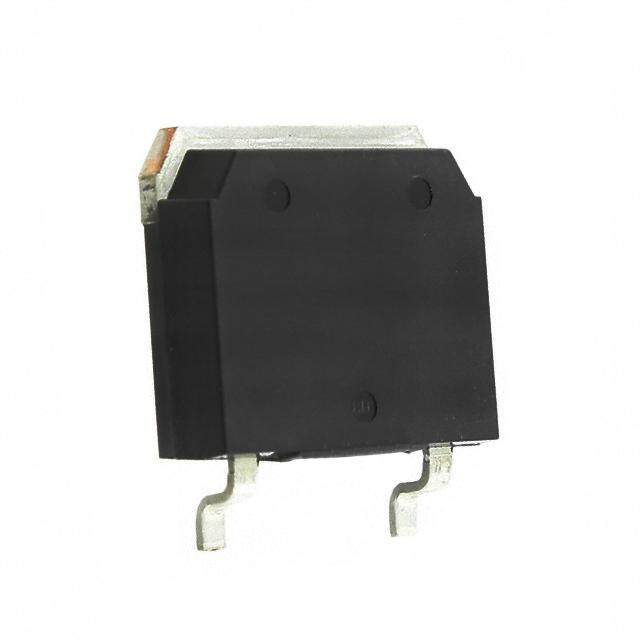
ICGOO电子元器件商城为您提供SIB417AEDK-T1-GE3由Vishay设计生产,在icgoo商城现货销售,并且可以通过原厂、代理商等渠道进行代购。 SIB417AEDK-T1-GE3价格参考。VishaySIB417AEDK-T1-GE3封装/规格:晶体管 - FET,MOSFET - 单, P-Channel 8V 9A (Tc) 2.4W (Ta), 13W (Tc) Surface Mount PowerPAK® SC-75-6L Single。您可以下载SIB417AEDK-T1-GE3参考资料、Datasheet数据手册功能说明书,资料中有SIB417AEDK-T1-GE3 详细功能的应用电路图电压和使用方法及教程。
SIB417AEDK-T1-GE3是Vishay Siliconix生产的一款N沟道功率MOSFET,属于单MOSFET器件,广泛应用于需要高效、低导通电阻和小尺寸封装的电源管理场合。该器件采用1.2mm×1.2mm的微型DFN1212封装,具有极低的导通电阻(RDS(on)),适合在空间受限且对能效要求较高的便携式设备中使用。

其典型应用场景包括:智能手机、平板电脑、可穿戴设备等消费类电子产品中的负载开关、电源开关和电池管理电路;各类移动设备中的热插拔控制与电源分配;以及DC-DC转换器中的同步整流环节,提升转换效率。此外,该MOSFET也适用于LED驱动电路、电机驱动模块和小型电源管理系统,因其快速开关特性可有效降低开关损耗。

得益于其高功率密度和优良的热性能,SIB417AEDK-T1-GE3能在有限空间内实现高效电能控制,特别适合高集成度、低电压、中低电流的应用环境。同时,该器件符合RoHS环保标准,支持无铅焊接工艺,适用于现代绿色电子产品制造。总体而言,它是一款面向高性能便携式电子设备的理想功率开关元件。
| 参数 | 数值 |
| 产品目录 | |
| 描述 | MOSFET P-CH 8V 9A PWRPACK |
| 产品分类 | FET - 单 |
| FET功能 | 标准 |
| FET类型 | MOSFET P 通道,金属氧化物 |
| 品牌 | Vishay Siliconix |
| 数据手册 | |
| 产品图片 |
|
| 产品型号 | SIB417AEDK-T1-GE3 |
| rohs | 无铅 / 符合限制有害物质指令(RoHS)规范要求 |
| 产品系列 | TrenchFET® |
| 不同Id时的Vgs(th)(最大值) | 1V @ 250µA |
| 不同Vds时的输入电容(Ciss) | 878pF @ 4V |
| 不同Vgs时的栅极电荷(Qg) | 18.5nC @ 5V |
| 不同 Id、Vgs时的 RdsOn(最大值) | 32 毫欧 @ 3A, 4.5V |
| 供应商器件封装 | PowerPAK® SC-75-6L 单 |
| 其它名称 | SIB417AEDK-T1-GE3CT |
| 功率-最大值 | 13W |
| 包装 | 剪切带 (CT) |
| 安装类型 | 表面贴装 |
| 封装/外壳 | PowerPAK® SC-75-6L |
| 标准包装 | 1 |
| 漏源极电压(Vdss) | 8V |
| 电流-连续漏极(Id)(25°C时) | 9A (Tc) |


- 商务部:美国ITC正式对集成电路等产品启动337调查
- 曝三星4nm工艺存在良率问题 高通将骁龙8 Gen1或转产台积电
- 太阳诱电将投资9.5亿元在常州建新厂生产MLCC 预计2023年完工
- 英特尔发布欧洲新工厂建设计划 深化IDM 2.0 战略
- 台积电先进制程称霸业界 有大客户加持明年业绩稳了
- 达到5530亿美元!SIA预计今年全球半导体销售额将创下新高
- 英特尔拟将自动驾驶子公司Mobileye上市 估值或超500亿美元
- 三星加码芯片和SET,合并消费电子和移动部门,撤换高东真等 CEO
- 三星电子宣布重大人事变动 还合并消费电子和移动部门
- 海关总署:前11个月进口集成电路产品价值2.52万亿元 增长14.8%


PDF Datasheet 数据手册内容提取
SiB417AEDK Vishay Siliconix P-Channel 1.2 V (G-S) MOSFET FEATURES PRODUCT SUMMARY • TrenchFET® Power MOSFET VDS (V) RDS(on) () Max. ID (A)g Qg (Typ.) (cid:129) Thermally Enhanced PowerPAK® 0.032 at VGS = - 4.5 V - 9a SC-75 Package 0.045 at VGS = - 2.5 V - 9a - Small Footprint Area - 8 0.063 at VGS = - 1.8 V - 9a 11.3 nC - Low On-Resistance 0.120 at VGS = - 1.5 V - 8.8 (cid:129) 100 % Rg Tested (cid:129) Typical ESD Protection 2500 V 0.230 at VGS = - 1.2 V - 6.4 (cid:129) Material categorization: For definitions of compliance PowerPAK SC-75-6L-Single please see www.vishay.com/doc?99912 1 APPLICATIONS D 2 (cid:129) Load Switch for Portable Devices, S D 3 Smart Phones, and Tablet PCs G - Low Voltage Drop D 6 - Space Savings D S 5 1.60 mm S 1.60 mm Marking Code G 4 B N X Part # code Ordering Information: X X X Lot Traceability D SiB417AEDK-T1-GE3 (Lead (Pb)-free and Halogen-free) and Date code P-Channel MOSFET ABSOLUTE MAXIMUM RATINGS (T = 25 °C, unless otherwise noted) A Parameter Symbol Limit Unit Drain-Source Voltage VDS - 8 V Gate-Source Voltage VGS ± 5 TC = 25 °C - 9a Continuous Drain Current (TJ = 150 °C) TTCA == 2750 °°CC ID - 7- .92ab, c TA = 70 °C - 5.7b, c A Pulsed Drain Current (t = 300 µs) IDM - 15 Continuous Source-Drain Diode Current TTCA == 2255 °°CC IS - -2 9ba, c T = 25 °C 13 C T = 70 °C 8.4 Maximum Power Dissipation TCA = 25 °C PD 2.4b, c W TA = 70 °C 1.6b, c Operating Junction and Storage Temperature Range TJ, Tstg - 55 to 150 °C Soldering Recommendations (Peak Temperature)d, e 260 THERMAL RESISTANCE RATINGS Parameter Symbol Typical Maximum Unit Maximum Junction-to-Ambientb, f t 5 s RthJA 41 51 °C/W Maximum Junction-to-Case (Drain) Steady State RthJC 7.5 9.5 Notes: a. Package limited. b. Surface mounted on 1" x 1" FR4 board. c. t = 5 s. d. See solder profile (www.vishay.com/doc?73257). The PowerPAK SC-75 is a leadless package. The end of the lead terminal is exposed copper (not plated) as a result of the singulation process in manufacturing. A solder fillet at the exposed copper tip cannot be guaranteed and is not required to ensure adequate bottom side solder interconnection. e. Rework conditions: manual soldering with a soldering iron is not recommended for leadless components. f. Maximum under steady state conditions is 105 °C/W. g. Based on T = 25 °C. C Document Number: 63899 For technical questions, contact: pmostechsupport@vishay.com www.vishay.com S12-2333-Rev. A, 01-Oct-12 1 This document is subject to change without notice. THE PRODUCTS DESCRIBED HEREIN AND THIS DOCUMENT ARE SUBJECT TO SPECIFIC DISCLAIMERS, SET FORTH AT www.vishay.com/doc?91000
SiB417AEDK Vishay Siliconix SPECIFICATIONS (T = 25 °C, unless otherwise noted) J Parameter Symbol Test Conditions Min. Typ. Max. Unit Static Drain-Source Breakdown Voltage VDS VGS = 0 V, ID = - 250 µA - 8 V VDS Temperature Coefficient VDS/TJ - 6.1 ID = - 250 µA mV/°C VGS(th) Temperature Coefficient VGS(th)/TJ 2.1 Gate-Source Threshold Voltage VGS(th) VDS = VGS, ID = - 250 µA - 0.35 - 1 V Gate-Source Leakage IGSS VDS = 0 V, VGS = ± 5 V ± 20 VDS = - 8 V, VGS = 0 V - 1 µA Zero Gate Voltage Drain Current IDSS VDS = - 8 V, VGS = 0 V, TJ = 55 °C - 10 On-State Drain Currenta ID(on) VDS - 5 V, VGS = - 4.5 V - 15 A VGS = - 4.5 V, ID = - 3 A 0.0265 0.0320 VGS = - 2.5 V, ID = - 3 A 0.0360 0.0450 Drain-Source On-State Resistancea RDS(on) VGS = - 1.8 V, ID = - 1 A 0.0500 0.0630 VGS = - 1.5 V, ID = - 0.5 A 0.0600 0.1200 VGS = - 1.2 V, ID = - 0.5 A 0.1000 0.2300 Forward Transconductancea gfs VDS = - 4 V, ID = - 7.4 A 18 S Dynamicb Input Capacitance Ciss 878 Output Capacitance Coss VDS = - 4 V, VGS = 0 V, f = 1 MHz 415 pF Reverse Transfer Capacitance Crss 735 Total Gate Charge Qg VDS = - 4 V, VGS = - 5 V, ID = - 7.4 A 12.3 18.5 11.3 17 nC Gate-Source Charge Qgs VDS = - 4 V, VGS = - 4.5 V, ID = - 7.4 A 1.35 Gate-Drain Charge Qgd 3.42 Gate Resistance Rg f = 1 MHz 1.3 6.5 13 Turn-On Delay Time td(on) 19 29 Rise Time tr VDD = - 4 V, RL = 0.68 18 27 ns Turn-Off Delay Time td(off) ID - 5.9 A, VGEN = - 4.5 V, Rg = 1 32 48 Fall Time tf 19 29 Drain-Source Body Diode Characteristics Continuous Source-Drain Diode Current IS TC = 25 °C - 9 A Pulse Diode Forward Current ISM - 15 Body Diode Voltage VSD IS = - 5.9 A, VGS = 0 V - 0.8 - 1.2 V Body Diode Reverse Recovery Time trr 32 48 ns Body Diode Reverse Recovery Charge Qrr 13 20 nC I = - 5.9 A, dI/dt = 100 A/µs, T = 25 °C F J Reverse Recovery Fall Time ta 14 ns Reverse Recovery Rise Time tb 18 Notes: a. Pulse test; pulse width 300 µs, duty cycle 2 %. b. Guaranteed by design, not subject to production testing. Stresses beyond those listed under “Absolute Maximum Ratings” may cause permanent damage to the device. These are stress ratings only, and functional operation of the device at these or any other conditions beyond those indicated in the operational sections of the specifications is not implied. Exposure to absolute maximum rating conditions for extended periods may affect device reliability. www.vishay.com For technical questions, contact: pmostechsupport@vishay.com Document Number: 63899 2 S12-2333-Rev. A, 01-Oct-12 This document is subject to change without notice. THE PRODUCTS DESCRIBED HEREIN AND THIS DOCUMENT ARE SUBJECT TO SPECIFIC DISCLAIMERS, SET FORTH AT www.vishay.com/doc?91000
SiB417AEDK Vishay Siliconix TYPICAL CHARACTERISTICS (25°C, unless otherwise noted) 0.015 10-2 T = 25 °C J 10-3 0.012 A) A) 10-4 urrent (m 0.009 Current ( 10-5 TJ = 150 °C ate C 0.006 Gate 10-6 - GGSS I - GSS 10-7 TJ = 25 °C I 0.003 10-8 0.000 10-9 0 2 4 5 7 9 0 3 6 9 12 VGS - Gate-Source Voltage (V) VGS - Gate-to-Source Voltage (V) Gate Source Voltage vs. Gate Current Gate Source Voltage vs. Gate Current 15 1 V = 5V thru 2V GS 12 0.8 ent (A) 9 nt (A) 0.6 Curr VGS = 1.5 V urre I - Drain D 6 - Drain CD 0.4 TC = 25 °C I 3 0.2 T = 125 °C V = 1 V C GS T = - 55 °C C 0 0 0 0.5 1 1.5 2 0 0.25 0.5 0.75 1 1.25 VDS - Drain-to-Source Voltage (V) VGS - Gate-to-Source Voltage (V) Output Characteristics Transfer Characteristics 0.2 1500 V = 1.2 V GS 1200 Ω) 0.15 Resistance ( 0.1 VGS = 1.5 V citance (pF) 900 Ciss R - On-DS(on) 0.05 VGS = 1.8 V VGS = 2.5 V C - Capa 600 Crss Coss 300 V = 4.5 V GS 0 0 0 3 6 9 12 15 0 2 4 6 8 V - Drain-to-Source Voltage (V) I - Drain Current (A) DS D On-Resistance vs. Drain Current and Gate Voltage Capacitance Document Number: 63899 For technical questions, contact: pmostechsupport@vishay.com www.vishay.com S12-2333-Rev. A, 01-Oct-12 3 This document is subject to change without notice. THE PRODUCTS DESCRIBED HEREIN AND THIS DOCUMENT ARE SUBJECT TO SPECIFIC DISCLAIMERS, SET FORTH AT www.vishay.com/doc?91000
SiB417AEDK Vishay Siliconix TYPICAL CHARACTERISTICS (25°C, unless otherwise noted) 5 1.4 I = 3 A I = 7.4 A D V = 4.5 V D GS d) ce Voltage (V) 34 VDS = 2 V VDS = 4 V ance (Normalize 11..1247 VGS = 2.5 V ur st e-to-So 2 VDS = 6.4 V On-Resi 1.01 V - GatGS 1 R - DS(on) 0.88 0 0.75 0 3.5 7 10.5 14 - 50 - 25 0 25 50 75 100 125 150 Qg - Total Gate Charge (nC) TJ - Junction Temperature (°C) Gate Charge On-Resistance vs. Junction Temperature 100 0.120 I = 3 A D urce Current (A) 10 TJ = 150 °C On-Resistance (Ω) 00..006900 TJ = 125 °C I - SoS 1 T = 25 °C R - DS(on) 0.030 TJ = 25 °C J 0.1 0.000 0.0 0.3 0.6 0.9 1.2 0 1 2 3 4 5 VSD - Source-to-Drain Voltage (V) VGS - Gate-to-Source Voltage (V) Soure-Drain Diode Forward Voltage On-Resistance vs. Gate-to-Source Voltage 0.7 20 I = 250 μA D 0.6 15 V) 0.5 (W) V (GS(th) 0.4 Power 10 5 0.3 0.2 0 - 50 - 25 0 25 50 75 100 125 150 0.001 0.01 0.1 1 10 100 T - Temperature (°C) Time (s) J Threshold Voltage Single Pulse Power, Junction-to-Ambient www.vishay.com For technical questions, contact: pmostechsupport@vishay.com Document Number: 63899 4 S12-2333-Rev. A, 01-Oct-12 This document is subject to change without notice. THE PRODUCTS DESCRIBED HEREIN AND THIS DOCUMENT ARE SUBJECT TO SPECIFIC DISCLAIMERS, SET FORTH AT www.vishay.com/doc?91000
SiB417AEDK Vishay Siliconix TYPICAL CHARACTERISTICS (25°C, unless otherwise noted) 100 20 10 Limited by RDS(on)* 100 μs n Current (A) 1 11110 00m0 m ssm, s1s s Current (A) 1105 ai DC n Dr 0.1 ai - ID - DrD I 5 0.01 T = 25 °C A Single Pulse BVDSS Limited 0.001 0 0.1 1 10 0 25 50 75 100 125 150 VDS - Drain-to-Source Voltage (V) T - Case Temperature (°C) * V > minimum V at which R is specified C GS GS DS(on) Safe Operating Area, Junction-to-Case Current Derating** 1.5 16 1.2 12 W) 0.9 W) ( ( wer wer 8 Po 0.6 Po 4 0.3 0.0 0 0 25 50 75 100 125 150 0 25 50 75 100 125 150 TA-AmbientTemperature(°C) TC-CaseTemperature(°C) Power Junction-to-Ambient Power Junction-to-Case ** The power dissipation P is based on T = 150 °C, using junction-to-case thermal resistance, and is more useful in settling the upper D J(max.) dissipation limit for cases where additional heatsinking is used. It is used to determine the current rating, when this rating falls below the package limit. Document Number: 63899 For technical questions, contact: pmostechsupport@vishay.com www.vishay.com S12-2333-Rev. A, 01-Oct-12 5 This document is subject to change without notice. THE PRODUCTS DESCRIBED HEREIN AND THIS DOCUMENT ARE SUBJECT TO SPECIFIC DISCLAIMERS, SET FORTH AT www.vishay.com/doc?91000
SiB417AEDK Vishay Siliconix TYPICAL CHARACTERISTICS (25°C, unless otherwise noted) 1 Duty Cycle = 0.5 nt e Transiance 0.2 ctive mped 0.1 Notes: ed Effeermal I 0.1 0.05 PDM alizTh 0.02 t1 Norm 1. Duty Cycle,t 2D = tt12 Single Pulse 2. Per Unit Base = RthJA = 105 °C/W 3. TJM - TA = PDMZthJA(t) 4. Surface Mounted 0.01 10-4 10-3 10-2 10-1 1 10 100 1000 Square Wave Pulse Duration (s) Normalized Thermal Transient Impedance, Junction-to-Ambient 1 Duty Cycle = 0.5 nt e Transiance ctive mped 0.2 ed Effeermal I 0.1 zh aliT 0.05 m or 0.02 N Single Pulse 0.1 10-4 10-3 10-2 10-1 Square Wave Pulse Duration (s) Normalized Thermal Transient Impedance, Junction-to-Case Vishay Siliconix maintains worldwide manufacturing capability. Products may be manufactured at one of several qualified locations. Reliability data for Silicon Technology and Package Reliability represent a composite of all qualified locations. For related documents such as package/tape drawings, part marking, and reliability data, see www.vishay.com/ppg?63899. www.vishay.com For technical questions, contact: pmostechsupport@vishay.com Document Number: 63899 6 S12-2333-Rev. A, 01-Oct-12 This document is subject to change without notice. THE PRODUCTS DESCRIBED HEREIN AND THIS DOCUMENT ARE SUBJECT TO SPECIFIC DISCLAIMERS, SET FORTH AT www.vishay.com/doc?91000
Package Information Vishay Siliconix PowerPAK® SC75-6L e b e b PIN1 PIN2 PIN3 PIN1 PIN2 PIN3 L L D2 K4 K 2 1 E 1 1 E D1 3 E D1 D1 E E K K PIN6 PIN5 PIN4 PIN6 PIN5 PIN4 K3 K1 KK22 K2 K1 K2 BACKSIDE VIEW OF SINGLE BACKSIDE VIEW OF DUAL D A Notes: 1. All dimensions are in millimeters 2. Package outline exclusive of mold flash and metal burr 3. Package outline inclusive of plating E A1 C Z z DETAIL Z SINGLE PAD DUAL PAD DIM MILLIMETERS INCHES MILLIMETERS INCHES Min Nom Max Min Nom Max Min Nom Max Min Nom Max A 0.675 0.75 0.80 0.027 0.030 0.032 0.675 0.75 0.80 0.027 0.030 0.032 A1 0 - 0.05 0 - 0.002 0 - 0.05 0 - 0.002 b 0.18 0.25 0.33 0.007 0.010 0.013 0.18 0.25 0.33 0.007 0.010 0.013 C 0.15 0.20 0.25 0.006 0.008 0.010 0.15 0.20 0.25 0.006 0.008 0.010 D 1.53 1.60 1.70 0.060 0.063 0.067 1.53 1.60 1.70 0.060 0.063 0.067 D1 0.57 0.67 0.77 0.022 0.026 0.030 0.34 0.44 0.54 0.013 0.017 0.021 D2 0.10 0.20 0.30 0.004 0.008 0.012 E 1.53 1.60 1.70 0.060 0.063 0.067 1.53 1.60 1.70 0.060 0.063 0.067 E1 1.00 1.10 1.20 0.039 0.043 0.047 0.51 0.61 0.71 0.020 0.024 0.028 E2 0.20 0.25 0.30 0.008 0.010 0.012 E3 0.32 0.37 0.42 0.013 0.015 0.017 e 0.50 BSC 0.020 BSC 0.50 BSC 0.020 BSC K 0.180 TYP 0.007 TYP 0.245 TYP 0.010 TYP K1 0.275 TYP 0.011 TYP 0.320 TYP 0.013 TYP K2 0.200 TYP 0.008 TYP 0.200 BSC 0.008 TYP K3 0.255 TYP 0.010 TYP K4 0.300 TYP 0.012 TYP L 0.15 0.25 0.35 0.006 0.010 0.014 0.15 0.25 0.35 0.006 0.010 0.014 T 0.03 0.08 0.13 0.001 0.003 0.005 ECN: C-07431 − Rev. C, 06-Aug-07 DWG: 5935 Document Number: 73000 www.vishay.com 06-Aug-07 1
Application Note 826 Vishay Siliconix RECOMMENDED PAD LAYOUT FOR PowerPAK® SC75-6L Single 1.250 (0.049) 0.250 (0.01) 0.250 (0.01) 0.500 (0.02) 0.400 (0.016) 0.300 (0.012) 0.180 (0.007) 0.370 (0.015) (0.043) 0.620 (0.024) 1.700 (0.067) 1.100 2.000 (0.079) 0.200 (0.008) 0.300 (0.012) 0.300 (0.012) 1 0.545 (0.021) 0.250 (0.01) 0.670 (0.026) 2.000 (0.079) Dimensions in mm/(Inches) Return to Index A P P L I C A T I O N N O T E Document Number: 70488 www.vishay.com Revision: 21-Jan-08 13
Legal Disclaimer Notice www.vishay.com Vishay Disclaimer ALL PRODUCT, PRODUCT SPECIFICATIONS AND DATA ARE SUBJECT TO CHANGE WITHOUT NOTICE TO IMPROVE RELIABILITY, FUNCTION OR DESIGN OR OTHERWISE. Vishay Intertechnology, Inc., its affiliates, agents, and employees, and all persons acting on its or their behalf (collectively, “Vishay”), disclaim any and all liability for any errors, inaccuracies or incompleteness contained in any datasheet or in any other disclosure relating to any product. Vishay makes no warranty, representation or guarantee regarding the suitability of the products for any particular purpose or the continuing production of any product. To the maximum extent permitted by applicable law, Vishay disclaims (i) any and all liability arising out of the application or use of any product, (ii) any and all liability, including without limitation special, consequential or incidental damages, and (iii) any and all implied warranties, including warranties of fitness for particular purpose, non-infringement and merchantability. Statements regarding the suitability of products for certain types of applications are based on Vishay’s knowledge of typical requirements that are often placed on Vishay products in generic applications. Such statements are not binding statements about the suitability of products for a particular application. It is the customer’s responsibility to validate that a particular product with the properties described in the product specification is suitable for use in a particular application. Parameters provided in datasheets and / or specifications may vary in different applications and performance may vary over time. All operating parameters, including typical parameters, must be validated for each customer application by the customer’s technical experts. Product specifications do not expand or otherwise modify Vishay’s terms and conditions of purchase, including but not limited to the warranty expressed therein. Except as expressly indicated in writing, Vishay products are not designed for use in medical, life-saving, or life-sustaining applications or for any other application in which the failure of the Vishay product could result in personal injury or death. Customers using or selling Vishay products not expressly indicated for use in such applications do so at their own risk. Please contact authorized Vishay personnel to obtain written terms and conditions regarding products designed for such applications. No license, express or implied, by estoppel or otherwise, to any intellectual property rights is granted by this document or by any conduct of Vishay. Product names and markings noted herein may be trademarks of their respective owners. © 2017 VISHAY INTERTECHNOLOGY, INC. ALL RIGHTS RESERVED Revision: 08-Feb-17 1 Document Number: 91000